background image

1A LOWDROP OUT VOLTAGE REGULATOR (ADJUSTABLE & FIXED)          LM1117

FEATURES

● Output Current up to 1 A

● Low Dropout Voltage ( 700mV at 1A Output Current )

● Three Terminal Adjustable or Fixed 1.5V, 1.8V, 2.5V, 2.85V,
     3.0V, 3.3V, 5.0V
● 2.85V Device for SCSI-II Active Terminator

● 0.04% Line Regulaion, 0.1% Load Regulation

● Very Low Quiescent Current
● Internal Current andTerminal Limit
● Logic-Controlled Electronics Shutdown
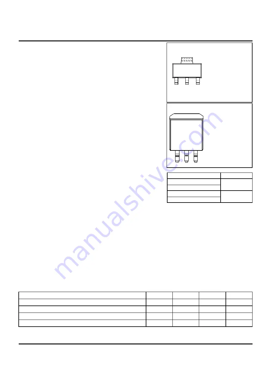
● Surface Mount Package SOT-223 & TO-263 (D2-Pack)
● 100% Thermal Limit Burn-In

APPLICATION

● Active SCSI Terminators

● Portable/Plan Top/Notebook Computers
● High Efficiency Linear Regulators
● SMPS Post Regulators

ORDERING INFORMATION

● Mother B/D Clock Supplies

     Package

● Disk Drives
● Battery Chargers

DESCRIPTION

(X=Output Voltage=1.5V, 1.8V, 2.5V, 2.85V,
  '3.0V, 3.3V, 5.0V, Adjustable=AD)

The LM1117 is a low power positive-voltage regulator designed to meet 1A output current and comply
with SCSI-II specifications with a fixed output voltage of 2.85V.  This device is an excellent choice for use
in battery-powered applications, as active terminators for the SCSI bus, and portable computers.
The LM1117 features very low quiescent current and very 

low dropout voltage of 700mV at a full load

 and

lower as output current decreases.  LM1117 is available as an adjustable or fixed 1.5V, 1.8V, 2.5V, 2.85V,  
3.0V, 3.3V, and 5.0V output voltages.
The LM1117 is offered in a 3-pin surface mount package SOT-223 & TO-263.  The output capacitor of
10㎌ or larger is needed for output stability of LM1117 as required by most of the other regulator circuits.

ABSOLUTE MAXIMUM RATINGS

HTC

  LM1117T

  LM1117T-XX

  TO-263 (D2)

         Device (Marking)

  SOT-223

  LM1117S

  LM1117S-XX

MIN.

UNIT

V

0

7

125

-65

150

Lead Temperature (Soldering, 5 Seconds) 

T

SOL

1

CHARACTERISTIC

DC Input Voltage

Operating Junction Temperature Range

SYMBOL

V

IN

T

OPR

Storage Temperature Range

T

STG

MAX.

260

   1          2         3

SOT-223 PKG (FRONT VIEW)

PIN FUNCTION
1. Adj/Gnd
2. Vout
3. Vin

TO-263 (D2 PKG, FRONT VIEW)

PIN FUNCTION
 1. Adj/Gnd
 2. Vout
 3. Vin

1      2      3

harman/kardon

AVR137/230 Service Manual

Page 53 of 87

Summary of Contents for AVR137/230

Page 1: ...R PINOUTS 35 BASIC SPECIFICATIONS 4 PCB DRAWINGS 72 TROUBLESHOOTING GUIDE 5 BLOCK DIAGRAM 78 PROCESSOR RESET 5 WIRING DIAGRAM 79 PACKAGE LIST AND PARTS 6 AMP BIAS ADJUSTMENT 80 DISASSEMBLY 7 SCHEMATIC...

Page 2: ...ower to the unit under test 2 After removing an electrical assembly equipped with ES devices place the assembly on a conductive surface such as aluminum foil to prevent electrostatic charge build up o...

Page 3: ...rol shaft etc Plug the AC line cord of the appliance directly into a 120V AC 60Hz outlet and turn the AC power switch on Any current measured must not exceed o 5mA ANY MEASUREMENTS NOT WITHIN THE LIMI...

Page 4: ...on 35dB 1kHz Selectivity 400kHz 70dB Image Rejection 80dB IF Rejection 90dB AM Tuner Section Frequency Range 522 1620kHz Signal to Noise Ratio 45dB Usable Sensitivity Loop 500 V Distortion 1kHz 50 Mod...

Page 5: ...ck to see if outlet is switch controlled Display lights but no sound Intermittent input connections Make certain that all input and speaker or picture connections are secure Mute is on Press Mute butt...

Page 6: ...G CSA1A027Z AM LOOP ANTENNA ASS Y 1 CABR03P3 BATTERY 3 COVER ASS Y CGRAVR130 230ZA POLY BAG 1 12 7 2 3 AM LOOP ANTENNA ASS Y BATTERY ASS Y 4 FM 1 POLE ANT 5 COVER ASS Y 6 BOOKLET INFORMATION 9 MANUAL...

Page 7: ...8 7 5 6 8 9 4 3 2 1 Remove the Screws 2 Removing the Front Panel 1 9 6 3 4 7 Remove the Screws 4 Removing the Main PCB 1 2 5 1 7 13 18 1 18 Remove the Screws 10 9 8 14 7 6 5 15 16 17 3 Removing the R...

Page 8: ...e BN84 5P on the Fip PCB 37 1 5 Remove 8 screws S2 S14 and then remove the Volume PCB 37 6 4 PHONE PCB 37 5 REMOVAL 1 Remove the Top cabinet referring to the previous step 1 2 Remove the Front Panel A...

Page 9: ...ut PCB 39 1 and connector CN12 21p on the main PCB 38 1 10 Disconnect the card cable between connector CN11 13p on the Input PCB 39 1 and connector CN11 13p on the main PCB 38 1 11 Disconnect connecto...

Page 10: ...P on the Main PCB 38 1 from connector CN89 on Regulator PCB A 40 2 10 Disconnect the lead wire BN19 3P BN20 4P on the Main PCB 38 1 from connector CN19 3P CN20 4P on TRANS PCB 40 4 11 Remove 11screws...

Page 11: ...N FILTER FIP WINDOW ASS Y BRACKET SIDE PANEL FRONT NO 2 1 HOLDER VOLUME CAP VOLUME DESCRIPTION CGL1A222 CGUAVR132 230 CGW1A427RDZH43 CBC1A158MBZG27 CBT1A1026MMZG27 CBT1A1028MBYG27 CMD2A443 KGB1A158Z C...

Page 12: ...S IN 1 BATTERY 3 CARTAVR137 REMOCON TRANSMITTER ASS Y ASS Y 1 CGRAVR130 2 COVER ASS Y COVER 1 CGR1A331M7H COVER A COVER 1 CGR1A332M7H COVER B COVER 1 CPS1A676 PAD COVER PAD 1 CQE1A220Z SHEET FRONT COV...

Page 13: ...PF 50V K 1 C863 HCBS1H101KB CAP CERAMIC 100PF 50V K 1 C866 CCEA1HKS100 CAP ELECT 10UF 50V SMALL SIZE 1 C867 CCEA1HKS100 CAP ELECT 10UF 50V SMALL SIZE 1 C868 CCEA1EKS470 CAP ELECT 47UF 25V 1 C869 CCEA1...

Page 14: ...1 R806 CRD20TJ472T RES CARBON 4 7K OHM 1 5W J 1 R824 CRD20TJ221T RES CARBON 220 OHM 1 5W J 1 R825 CRD20TJ681T RES CARBON 680 OHM 1 5W J 1 R828 CRD20TJ221T RES CARBON 220 OHM 1 5W J 1 R829 CRD20TJ681T...

Page 15: ...WAFER WAFER 1 CN85 CJP02GA19ZY WAFER 2PIN WAFER 1 CN86 CJP02GA89ZM WAFER WAFER 1 CN88 CJP04GB46ZY WAFER WAFER 1 CN89 CJP04GB46ZY WAFER WAFER 1 D701 CVD52CSBBCE L E D BLUE L E D 1 D703 CVD52CSBBCE L E...

Page 16: ...CCEA1HH100T CAP ELECT 10UF 50V 1 C506 CCKT1H331KB CAP CERAMIC 330PF 50V 1 C507 HCBS1H331KB CAP CERAMIC 330PF 50V 1 C508 HCBS1H331KB CAP CERAMIC 330PF 50V 1 C509 CCKT1H331KB CAP CERAMIC 330PF 50V 1 C51...

Page 17: ...0V J 1 C997 HCQI1H473JZ CAP MYLAR 0 047UF 50V J 1 C999 CCFT1H223ZF CAP CERAMIC 0 022UF 50V ZF 1 D501 CVD1SS133MT DIODE 1SS133 1 D502 CVD1SS133MT DIODE 1SS133 1 D503 CVD1SS133MT DIODE 1SS133 1 D504 CVD...

Page 18: ...2785Y 1 Q951 HVTKRC107MT T R KRC107M 1 Q952 HVTKRA107MT T R KRA107M 1 Q960 HVTKRC107MT T R KRC107M 1 Q961 HVTKTA1024Y T R KTA1024YT 1 Q991 HVTKRC107MT T R KRC107M 1 Q992 HVTKRA107MT T R KRA107M 1 R501...

Page 19: ...TJ561T RES CARBON 560 OHM 1 5W J 1 R576 CRD20TJ100T RES CARBON 10 OHM 1 5W J 1 R577 CRD20TJ100T RES CARBON 10 OHM 1 5W J 1 R578 CRD20TJ100T RES CARBON 10 OHM 1 5W J 1 R579 CRD20TJ100T RES CARBON 10 OH...

Page 20: ...CARBON 5 6K OHM 1 5W J 1 R686 CRD20TJ103T RES CARBON 10K OHM 1 5W J 1 R687 CRD20TJ103T RES CARBON 10K OHM 1 5W J 1 R688 CRD20TJ103T RES CARBON 10K OHM 1 5W J 1 R689 CRD20TJ103T RES CARBON 10K OHM 1 5...

Page 21: ...JP08GA130Z WAFER WAFER 1 CN11 CJP13GA117Z WAFER CARD CABLE WAFER 1 CN12 CJP21GA115Z WAFER CARD CABLE WAFER 1 CN61 CJP02GA01ZY WAFER STRAIGHT 2PIN WAFER 1 CN62 CJP02GA01ZY WAFER STRAIGHT 2PIN WAFER 1 C...

Page 22: ...R POSISTOR P42T7D330BW20 1 T902 CLT5J033YE TRANS SUB SR 68 1 Ref CMYAVR137 2 HEAT SINK ASS Y Value Qty CMYAVR144 HEAT SINK ASS Y ASS Y 1 CTW3 8JR SCREW SCREW 2 C8AGB288 BOND MAX BOND 10 2 CHD1A012R SC...

Page 23: ...CQI1H103JZ CAP MYLAR 0 01UF 50V J 1 C927 HCQI1H103JZ CAP MYLAR 0 01UF 50V J 1 C928 HCQI1H103JZ CAP MYLAR 0 01UF 50V J 1 C931 HCQI1H473JZ CAP MYLAR 0 047UF 50V J 1 C932 HCQI1H473JZ CAP MYLAR 0 047UF 50...

Page 24: ...1 5W J 1 R921 CRD20TJ153T RES CARBON 15K OHM 1 5W J 1 R922 CRD20TJ153T RES CARBON 15K OHM 1 5W J 1 R923 CRD25TJ153T RES CARBON 15K OHM 1 4W J 1 R924 CRD20TJ153T RES CARBON 15K OHM 1 5W J 1 R925 CRD20...

Page 25: ...CARBON 300OHM 1 5W J 1 R895 CRD20TJ301T RES CARBON 300OHM 1 5W J 1 R896 CRD20TJ301T RES CARBON 300OHM 1 5W J 1 R897 CRD20TJ301T RES CARBON 300OHM 1 5W J 1 Ref Part Number Description Value Qty COP1193...

Page 26: ...M 1 5W J 1 R453 CRD20TJ750T RES CARBON 75 OHM 1 5W J 1 R461 CRD20TJ102T RES CARBON 1K OHM 1 5W J 1 R466 CRD20TJ102T RES CARBON 1K OHM 1 5W J 1 R471 CRD20TJ102T RES CARBON 1K OHM 1 5W J 1 R491 CRD20TJ7...

Page 27: ...C CAP CHIP 3300PF 1 C312 CCUS1H332KC CAP CHIP 3300PF 1 C313 CCUS1H332KC CAP CHIP 3300PF 1 C314 CCUS1H332KC CAP CHIP 3300PF 1 C317 CCUS1H223KC CAP CHIP 0 022UF 1 C318 CCUS1H223KC CAP CHIP 0 022UF 1 C31...

Page 28: ...719 CCUS1H104KC CAP CHIP 0 1UF 1 C722 CCUS1H104KC CAP CHIP 0 1UF 1 C723 CCUS1H473KC CAP CHIP 0 047UF 1 C725 CCUS1H104KC CAP CHIP 0 1UF 1 C727 CCUS1H104KC CAP CHIP 0 1UF 1 C729 CCUS1H104KC CAP CHIP 0 1...

Page 29: ...103 RES ARRAY 10K 1608 10K OHM 1608 4 1 RN62 CRJ104DJ103 RES ARRAY 10K 1608 10K OHM 1608 4 1 RN63 CRJ104DJ103 RES ARRAY 10K 1608 10K OHM 1608 4 1 RN64 CRJ104DJ101 RES CHIP NETWORK 1 16W 100 ohm 1608 4...

Page 30: ...1 R249 CRJ10DJ474T RES CHIP 470K OHM 1 R250 CRJ10DJ103T RES CHIP 10K OHM 1 R253 CRJ10DJ4R7T RES CHIP 4 7 OHM 1 R254 CRJ10DJ4R7T RES CHIP 4 7 OHM 1 R256 CRJ10DJ4R7T RES CHIP 4 7 OHM 1 R257 CRJ10DJ4R7T...

Page 31: ...10DJ104T RES CHIP 100K OHM 1 R371 CRJ10DJ512T RES CHIP 5 1K OHM 1 R372 CRJ10DJ512T RES CHIP 5 1K OHM 1 R373 CRJ10DJ512T RES CHIP 5 1K OHM 1 R374 CRJ10DJ103T RES CHIP 10K OHM 1 R375 CRJ10DJ512T RES CHI...

Page 32: ...M 1 R776 CRJ10DJ332T RES CHIP 3 3K OHM 1 R777 CRJ10DJ102T RES CHIP 1K OHM 1 R778 CRJ10DJ103T RES CHIP 10K OHM 1 R782 CRJ10DJ272T RES CHIP 2 7K OHM 1 R783 CRJ10DJ272T RES CHIP 2 7K OHM 1 R784 CRJ10DJ47...

Page 33: ...16V 1 C628 CCEA1CH101T CAP ELECT 100UF 16V 1 C630 CCEA1CH101T CAP ELECT 100UF 16V 1 C703 CCEA1CH101T CAP ELECT 100UF 16V 1 C706 CCEA1CH101T CAP ELECT 100UF 16V 1 C717 CCEA1CH101T CAP ELECT 100UF 16V 1...

Page 34: ...WAFER STRAIGHT 5PIN WAFER 1 CN72 CJP17GA117Z WAFER WAFER 1 C732 CCEA0JKR322 CAP ELECT 2200UF 6 3V 1 IC36 HVIL7808CP I C REGULATOR 8V 1 IC37 HVINJM7908F I C REGULATOR 1 JK11 CJJ4R019W TERMINAL IN OUT T...

Page 35: ...age VCE V Collector Curr ent I C A Without Heatsink Natural Cooling D C 100m s 10m s 80 60 40 20 3 5 0 0 25 50 75 100 125 150 Ambient Temperature Ta C M aximu m Power Dissipat io n P C W W i t h I n f...

Page 36: ...4V 0 2 0 5 5 8 1 Collector Current IC A DC C urrent G ain h FE 1000 500 5000 10000 50000 125 C 25 C 30 C 0 02 0 1 1 8 0 20 40 120 100 80 60 Cut off F req uenc y f T MH Z VCE 12V Emitter Current IE A T...

Page 37: ...d with sub micron silicon gate and double layer metal wiring C2MOS technology The internal circuit is composed of 3 stages including buffer output which enables high noise immunity and stable output T...

Page 38: ...d with sub micron silicon gate and double layer metal wiring C2MOS technology The internal circuit is composed of 3 stages including buffer output which enables high noise immunity and stable output T...

Page 39: ...E AND FUNCTION 1 3 5 9 11 13 1A to 6A data inputs 2 4 6 8 10 12 1Y to 6Y data outputs 7 GND ground 0 V 14 VCC positive supply voltage Fig 1 Pin configuration Fig 2 Logic symbol Fig 3 IEC logic symbol...

Page 40: ...52 51 50 49 48 47 46 45 44 43 42 41 80 79 78 77 76 75 74 73 72 71 70 69 68 67 66 65 64 63 62 61 1 2 3 4 5 6 7 8 9 10 11 12 13 14 15 16 17 18 19 20 INT1 BOUT TVDD DVDD DVSS XTO XTI TEST3 MCKO2 MCKO1 CO...

Page 41: ...harman kardon AVR137 230 Service Manual Page 41 of 87...

Page 42: ...CES DESCRIPTION The HCF4053B is a monolithic integrated circuit fabricated in Metal Oxide Semiconductor technology available in DIP and SOP packages The HCF4053B analog multiplexer demultiplexer is a...

Page 43: ...harman kardon AVR137 230 Service Manual Page 43 of 87...

Page 44: ...ESCRIPTION PIN PIN NAME DESCRIPTION CLK Clock The system clock input All other inputs are referenced to the SDRAM on the rising edge of CLK CKE Clock Enable Controls internal clock signal and when dea...

Page 45: ...harman kardon AVR137 230 Service Manual Page 45 of 87...

Page 46: ...harman kardon AVR137 230 Service Manual Page 46 of 87...

Page 47: ...T L7808C L7808CV L7808C V L7808CD2T L7808CP L7808CF L7808CT L7885C L7885CV L7885CD2T L7885CP L7885CF L7885CT L7809C L7809CV L7809C V L7809CD2T L7809CP L7809CF L7809CT L7810C L7810CV L7810CD2T L7810CP...

Page 48: ...T L7808C L7808CV L7808C V L7808CD2T L7808CP L7808CF L7808CT L7885C L7885CV L7885CD2T L7885CP L7885CF L7885CT L7809C L7809CV L7809C V L7809CD2T L7809CP L7809CF L7809CT L7810C L7810CV L7810CD2T L7810CP...

Page 49: ...T L7808C L7808CV L7808C V L7808CD2T L7808CP L7808CF L7808CT L7885C L7885CV L7885CD2T L7885CP L7885CF L7885CT L7809C L7809CV L7809C V L7809CD2T L7809CP L7809CF L7809CT L7810C L7810CV L7810CD2T L7810CP...

Page 50: ...7952CD2T L7906CD2T L7908CD2T L7912CD2T L7915CD2T L7918CD2T L7920CD2T L7922CD2T L7924CD2T L7905CP L7906CP L7908CP L7912CP L7915CP L7918CP L7920CP L7924CP L7905CT L7952CT L7906CT L7908CT L7912CT L7915CT...

Page 51: ...7952CD2T L7906CD2T L7908CD2T L7912CD2T L7915CD2T L7918CD2T L7920CD2T L7922CD2T L7924CD2T L7905CP L7906CP L7908CP L7912CP L7915CP L7918CP L7920CP L7924CP L7905CT L7952CT L7906CT L7908CT L7912CT L7915CT...

Page 52: ...Pin Assignment DIP16 MFP16 No 6037 2 8 LC72723 LC72723M Block Diagram harman kardon AVR137 230 Service Manual Page 52 of 87...

Page 53: ...fixed output voltage of 2 85V This device is an excellent choice for use in battery powered applications as active terminators for the SCSI bus and portable computers The LM1117 features very low qui...

Page 54: ...fixed output voltage of 2 85V This device is an excellent choice for use in battery powered applications as active terminators for the SCSI bus and portable computers The LM1117 features very low qui...

Page 55: ...in the same way Data transfers are terminated by a Stop condition after an Ack for Write and after a NoAck for Read Table 2 Signal Names Power On Reset VCC Lock Out Write Protect In order to prevent...

Page 56: ...1 12 13 14 15 16 32 31 30 29 28 27 26 25 24 23 22 20 19 18 17 DQ1 DQ9 A6 A5 DQ6 DQ13 44 39 38 37 36 35 34 33 A11 A10 DQ10 21 DQ12 40 43 1 42 41 A17 A8 A18 DQ3 DQ9 DQ2 A6 DQ0 W A3 RB DQ6 A8 A9 DQ13 A17...

Page 57: ...put voltages making them useful in a wide range of applications Each type employs internal current limiting thermal shut down and safe operating area protection making it essentially indestructible If...

Page 58: ...harman kardon AVR137 230 Service Manual Page 58 of 87...

Page 59: ...1V typ At Io 1A zInternal Excessive Voltage Protection Circuit zInternal Short Circuit Current Limit zInternal Thermal Overload Protection zBipolar Technology zPackage Outline TO 252 PIN CONFIGURATION...

Page 60: ...K DIAGRAM 13 9 7 5 3 20k 20k 20k 20k 16 10 14 2 1 15 11 8 12 6 4 6dB Amp 75 Driver S3 S2 S4 S1 20k 20k 20k S5 S6 S7 Vin1 Vin2 Vin3 Vin4 Vin5 SW3 SW4 SW5 SW1 SW2 V GND V Vout3 Vout2 Vout1 6dB Amp 6dB A...

Page 61: ...harman kardon AVR137 230 Service Manual Page 61 of 87...

Page 62: ...harman kardon AVR137 230 Service Manual Page 62 of 87...

Page 63: ...harman kardon AVR137 230 Service Manual Page 63 of 87...

Page 64: ...harman kardon AVR137 230 Service Manual Page 64 of 87...

Page 65: ...RIPTION TO 92 SOT 89 SOT 23 5 Pin No Symbol 1 OUT 2 VDD 3 GND 4 NC 5 NC Pin No Symbol 1 OUT 2 VDD 3 GND Pin No Symbol 1 OUT 2 VDD 3 GND 1 2 3 mark side 1 2 3 mark side 1 2 3 mark side 5 4 R 5VL 5 harm...

Page 66: ...IN DESCRIPTION TO 92 SOT 89 SOT 23 5 Pin No Symbol 1 OUT 2 VDD 3 GND 4 NC 5 NC Pin No Symbol 1 OUT 2 VDD 3 GND Pin No Symbol 1 OUT 2 VDD 3 GND 1 2 3 mark side 1 2 3 mark side 1 2 3 mark side 5 4 harma...

Page 67: ...l for the second Charge Pump Capacitor 6 V Inverted Voltage Terminal 7 T2OUT Second Transmitter Output Voltage 8 R2IN Second Receiver Input Voltage 9 R2OUT Second Receiver Output Voltage 10 T2IN Secon...

Page 68: ...harman kardon AVR137 230 Service Manual Page 68 of 87...

Page 69: ...harman kardon AVR137 230 Service Manual Page 69 of 87...

Page 70: ...harman kardon AVR137 230 Service Manual Page 70 of 87...

Page 71: ...harman kardon AVR137 230 Service Manual Page 71 of 87...

Page 72: ...harman kardon AVR137 230 Service Manual Page 72 of 87 AVR 137 230...

Page 73: ...harman kardon AVR137 230 Service Manual Page 73 of 87 AVR 137 230...

Page 74: ...harman kardon AVR137 230 Service Manual Page 74 of 87 AVR 137 230...

Page 75: ...harman kardon AVR137 230 Service Manual Page 75 of 87 AVR 137 230...

Page 76: ...harman kardon AVR137 230 Service Manual Page 76 of 87 AVR 137 230...

Page 77: ...harman kardon AVR137 230 Service Manual Page 77 of 87 AVR 137 230...

Page 78: ...harman kardon AVR137 230 Service Manual Page 78 of 87 AVR 137 230 BLOCK DIAGRAM...

Page 79: ...harman kardon AVR137 230 Service Manual Page 79 of 87 AVR 137 230 wiring diagram...

Page 80: ...ETER Connect to CN66 SL CN61 CEN CN64 SR CN63 FL CN65 SBL SL AVR132 144 145 CN62 FR CN67 SBR CN61 CN65 Adjust for Adjustment 25 92mV 5 CN64 25 92mV 5 25 92mV 5 25 92mV 5 25 92mV 5 CN63 CN62 Channel Fr...

Page 81: ...harman kardon AVR137 230 Service Manual Page 81 of 87 AVR 137 230...

Page 82: ...harman kardon AVR137 230 Service Manual Page 82 of 87 AVR 137 230...

Page 83: ...harman kardon AVR137 230 Service Manual Page 83 of 87 AVR 137 230...

Page 84: ...harman kardon AVR137 230 Service Manual Page 84 of 87 AVR 137 230...

Page 85: ...harman kardon AVR137 230 Service Manual Page 85 of 87 AVR 137 230...

Page 86: ...harman kardon AVR137 230 Service Manual Page 86 of 87 AVR 137 230...

Page 87: ...harman kardon AVR137 230 Service Manual Page 87 of 87 AVR 137 230...

Reviews: