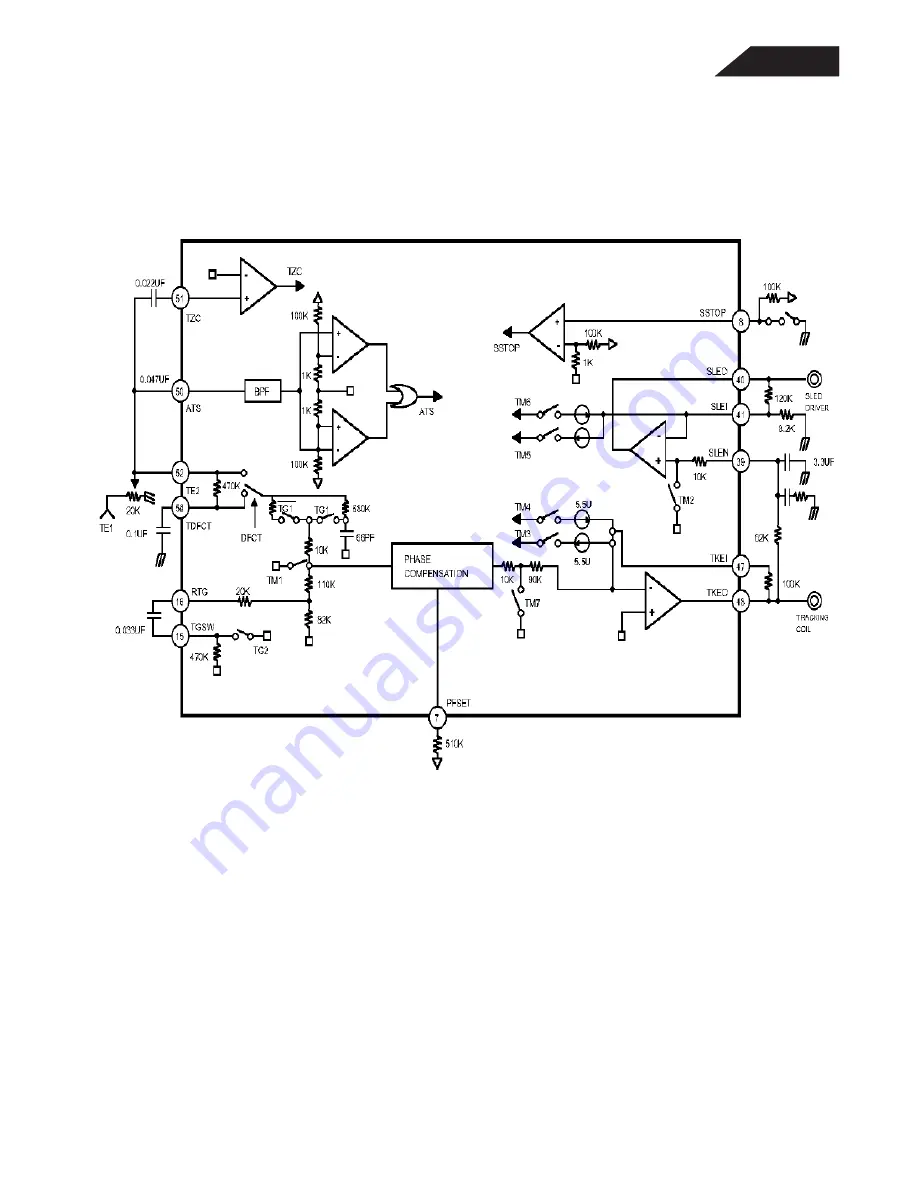
While the focus search is operating, the FS4 switch is ON and then focus error signal is isolated,
accordingly it is outputted by FSEO Pin (Pin48). When the FS2 switch is ON, the focus servo Loop is on
and then focus error is outputted through the focus servo Loop.
2. TRACKING AND SLED SERVO LOOP
The capacitor across RTG (Pin16) and TGSW (Pin15) reduces high frequency gain when the TG2 switch
is OFF. The Peak frequency of the tracking phase compensation is at about 1.2KHz when the resistor
connected to PFSET (Pin7) is 510K
Ω
. It is inversely proportional to the resistor connected to the Pin 7.
The tracking error signal is switched into low pass filter route formed by connecting a capacitor between
the built-in resistor at DFCT (470K
Ω
) and TDFCT (Pin54) as for tracking error signal.
FL8550
33
Summary of Contents for FL 8550
Page 12: ...FL8550 12 ...
Page 13: ...FL8550 13 ...
Page 14: ...FL8550 ...
Page 15: ...15 FL8550 ...
Page 16: ...FL8550 ...
Page 17: ...FL8550 ...
Page 38: ...KA9220C FL8550 38 ...
Page 39: ...FL8550 39 ...
Page 40: ...FL8550 40 ...
Page 41: ...FL8550 41 ...
Page 42: ...FL8550 42 ...
Page 43: ...FL8550 43 ...
Page 44: ...KS9284 FL8550 44 ...
Page 45: ...FL8550 45 ...
Page 46: ...FL8550 46 ...
Page 47: ...FL8550 47 ...
Page 48: ...FL8550 48 ...
Page 49: ...FL8550 49 ...
Page 59: ...Internal Block Diagram FL8550 59 ...
Page 60: ...Pin Arrangement FL8550 60 ...
Page 68: ...FL8550 68 ...
Page 69: ...FL8550 69 ...
Page 70: ...FL8550 70 ...
Page 71: ...FL8550 71 ...
Page 72: ...FL8550 72 ...
Page 73: ...FL8550 73 ...
Page 74: ...FL8550 FL8550 74 ...
Page 75: ...FL8550 75 ...
Page 76: ...FL8550 76 ...
Page 77: ...FL8550 77 ...
Page 78: ...78 FL8550 ...
Page 79: ...79 FL8550 ...


