background image

Technical Manual

The Harman Kardon

Model HD755 silver

COMPACT DISC PLAYER

DANGER

: Invisible laser radiation when open and interlock failed or defeated.

AVOID DIRECT EXPOSURE TO BEAM.

CONTENTS

Parts and Service Office

250 Crossways Park Dr., Woodbury, N.Y. 11797

1112-FL8350 P9603 1200  Printed in Hong Kong

1. LASER BEAM SAFETY PRECAUTIONS ............. 2
2. CONTROL AND FUNCTIONS ............................. 4
3. SPECIFICATIONS AND FEATURES ..................... 7
4. AUDIO CHARACTERISTICS TEST PROCEDURE 

.............................................................................. 9

5. CIRCUIT DESCRIPTION ....................................11
6. CRITICAL I.C. SPECIFICATION ........................ 15
7. PART LIST ......................................................... 41

9. BLOCK DIAGRAM ............................................. 54
10. SCHEMATIC DIAGRAMS .................................. 55
11. PCB LAYOUT ..................................................... 59
12. EXPLODED VIEW .............................................. 62
13. PACKING DRAWING ......................................... 63

*  Harman/ kardon continually strives to improve its products.  The HD750 Compact Disc Player design and 

specifications are subject to change and may differ from the published specifications and descriptions, but will 

always equal or exceed the original specifications unless otherwise stated.

8. TROUBLE SHOOTING GUIDE .......................... 48

Standby

HD755

Summary of Contents for HD 755

Page 1: ...FICATIONS AND FEATURES 7 4 AUDIO CHARACTERISTICS TEST PROCEDURE 9 5 CIRCUIT DESCRIPTION 11 6 CRITICAL I C SPECIFICATION 15 7 PART LIST 41 9 BLOCK DIAGRAM 54 10 SCHEMATIC DIAGRAMS 55 11 PCB LAYOUT 59 12 EXPLODED VIEW 62 13 PACKING DRAWING 63 Harman kardon continually strives to improve its products The HD750 Compact Disc Player design and specifications are subject to change and may differ from the...

Page 2: ...m coming from the pickup or allow it to strike against your skin This compact disc player uses a pickup that emits a laser beam The laser beam is emitted from the location shown in the figure When checking the laser diode be sure to keep your eyes at least 1 foot away from the pickup lens when the diode is turned on Do not look directly at the laser beam CAUTION Using controls and adjustment or do...

Page 3: ... can be damaged by electrostatic discharge from your clothes or your body Proper electrostatic grounding for service personal is required during servicing BEFORE REPAIRING THE COMPACT DISC PLAYER Preparation Human Body Grounding Many of the components used in this compact disc player including the laser pickup are sensitive to electrostatic discharge Service personal should be grounded with an ele...

Page 4: ...use Button Press this button to start the playback of a CD If the CD drawer is open pressing this button will automatically close the drawer When a disc is playing press this button once to momentarily stop a disc When the button is pressed again the disc will resume play at the point it was stopped A Intro Button Press this button to put the HD750 in teh Intro Scan mode When you press the button ...

Page 5: ...tal to analog converter for direct access to the digital signals of HD750 DO NOT connect this jack to the standard audio inputs of any device Remote Control Input Connect the out put of a remote infrared sensor or the remote control output of another compatible Harman Kardon product This will enable the remote con trol system to operate even when the front panel Remote Sensor is blocked It will al...

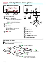
Page 6: ...Display Button Numeric Controls Clear Button Search Buttons Skip Buttons Stop Button Play Button Program Button Pause Button Check Button Time Button Random Button Repeat Button A B Button Power On Power Off Open Close Button 1 3 4 5 2 6 7 8 9 11 10 12 13 14 15 16 17 6 HD755 ...

Page 7: ...z 0dB no HDCD 1 0 Vrms 1dB Output Level 1KHz 0dB HDCD output 2 0Vrms 2dB Frequency Response 20Hz 20KHz reference 0 1dB 0 5 1 5dB THD 1KHz 0dB 30KHz Filter 0 006 0 01 THD 1KHz 0dB no any filter 0 03 0 08 THD 20Hz 20KHz 0dB 30KHz Filter 0 04 0 05 S N 1KHz 0dB A weighted A Filter 96dB 96dB Dynamic Range 95dB 95dB Channel Separation 1KHz 0dB 30KHz Filter 94dB 90dB Channel Balance 0 5dB 1 5dB De emphas...

Page 8: ...cal Limit Black Dot TCD 725B 1000um 600um Interruption MCD 131 900um 600um Finger print 75um 65um Vertical Deviation MCD 151 0 92mm 0 92mm Eccentricity TCD 712 140um 140um 8cm test disc TCD 783 Last Track Last Track Access Time 1st to last track YEDS18 4 sec 10 sec HD755 8 ...

Page 9: ...r to LEVEL mode 3 Select track 2 of the test disc and play the CD disc 4 The output voltage and gain of the R L channels are taken by pressing the respective buttons on the control board of Audio Analyzer Frequency Response 1 Set the mode of the filter to reference level mode 2 Select the track 3 4 5 and 6 of the test disc and run it under Play mode 3 Check the output of the R L Channels Total Har...

Page 10: ...dio analyzer to DIST Mode 3 Set the unit of the audio analyzer to dB mode 4 Play track 17of the test disc 5 The dynamic range should be A 60dB Channel Separation 1 Set the mode of the filter to DIST CH SP mode 2 Set the audio analyzer to LEVEL mode 3 Play the tracks 8 9 10 11 4 The measured results is the difference between L R channel De emphasis 1 Press the THRU button of the CD filter 2 Play th...

Page 11: ... balance voltage VTBAL from Pin 31 VTBAL varies with reference to the center voltage VREF2 1 65 V within 0 5 V The tracking gain will change according to the type of disc For normal disc or CDR disc VGCTRL is set to VREF2 for CDRW disc VGCTRL is set to VREF2 0 75 V At the same time the focus gain is changed too A B C D F PDIC E 32 31 28 21 30 23 25 24 GCTRL To Focus System TBAL Subtraction R10 TEN...

Page 12: ... voltage VFBAL from Pin 30 VFBAL varies with reference to the center voltage VREF2 1 65 V within 0 5 V The focus gain will change according to the type of disc For normal disc or CDR disc VGCTRL is set to VREF2 for CDRW disc VGCTRL is set to VREF2 0 75 V At the same time the tracking gain is changed too A B C D F PDIC E 36 34 28 29 27 26 GCTRL FBAL Subtraction R7 FEN C4 FEOUT VGCTRL C2 C3 R6 VFBAL...

Page 13: ...ll types of disc C38 connected to Pin 9 is for the AGC loop filter The RF Detection block detects the amplitude of the RF signal inputted from the EQ block Inputted RF signal is detected after passing through a high pass filter Detection level is changed in accrodance with the voltage of GCTRL Pin 28 The ENV detection block detects the fluctuation of the 3T composition in the RF signal which is ne...

Page 14: ...ntrolled current for getting regular output power thus the APC Auto Power Control circuit is composed Reference Power Supply A reference power supply for servo is built in The current capacity of the reference supply is about 3 mA VREF1 1 2 VCC1 2 5 V VREF2 1 2 VCC2 1 65 V where VCC1 5 V and VCC2 3 3 V 19 LD 2 1 VCC1 PD 170mV LASER UNIT C33 R18 Q1 LDON 20 R VCC1 R R 2 VREF1 22 R VCC2 R R 2 VREF2 1...

Page 15: ... check Built in subcode Q data register CIRC error detection and correction C1 decoder duplex error correction C2 decoder triplex error correction Built in 16 K bits of RAM for use in de interleaving Audio data interpolation Averaging or retention of previous values Digital attenuation 12 dB Audio data peak level detection function Digital audio interface EIAJ format Audio data serial interface fo...

Page 16: ...F WVEL PLAY PLLF2 BCLK LRCK SRDATA DV DD1 DV SS1 TX MCLK MDATA MLD SENSE FLOCK TLOCK BLKCK SQCK SUBQ DMUTE STAT RST SMCK PMCK LDON BDO RFDET TRCRS OFT VDET RFENV TE FE TBAL FBAL VREF FOD TRD KICK ECS ECM PC TVD TRV 61 62 63 64 65 66 67 68 69 70 71 72 73 74 75 76 77 78 79 80 40 39 38 37 36 35 34 33 32 31 30 29 28 27 26 25 24 23 22 21 60 59 58 57 56 55 54 53 52 51 50 49 48 47 46 45 44 43 42 41 1 2 3...

Page 17: ...LDON PLAY FLOCK TLOCK 40 42 11 12 26 KICK 21 TRV 16 DMUTE 1 BCLK 3 SRDATA 2 LRCK 23 PC 24 ECM 6 TX 64 IPFLAG 65 FLAG 22 TVD 27 TRD 28 FOD 31 TBAL 30 FBAL 43 WVEL 10 SENSE STAT X1 X2 MSEL CSEL PMCK FCLK SMCK VCOF2 58 79 77 59 20 63 19 CK384 EFM 54 VCOF 49 MDATA 8 MCLK 7 MLD 9 17 44 46 45 47 41 52 76 78 RSEL ARF PSEL DSLF PLLF2 48 PLLF 62 13 67 66 55 56 68 15 14 80 CLDCK BLKCK SUBC SBCK FLAG6 RESY 6...

Page 18: ...de block clock signal fBLKCK 75 Hz 14 SQCK I External clock input for subcode Q register 15 SUBQ O Subcode Q data output 16 DMUTE I Muting input Effective only for an output bit rate of 64 fs H level muting 17 STAT O Status signal CRC CLVS TTSTOP JCLVS SQOK FLAG6 SENSE FLOCK TLOCK rpm data and FCLV 18 RST I Reset input L level reset 19 SMCK O If MSEL is H level 8 4672 MHz clock signal output If MS...

Page 19: ...utput fPCK 4 3218 MHz or DSLB 54 VCOF2 I O VCO loop filter pin 55 SUBC O Subcode serial output 56 SBCK I Serial clock input for subcode serial output 57 VSS I Ground for oscillator circuit 58 X1 I Crystal oscillator circuit input output pins f 16 9344 MHz 33 8688 MHz 59 X2 O Crystal oscillator circuit output output pins f 16 9344 MHz 33 8688 MHz 60 VDD I Oscillator circuit power supply 61 BYTCK or...

Page 20: ... channel audio outputs 73 OUTL O Left channel audio output 74 AVSS1 I Ground for analog circuits common use for left and right channel audio outputs 75 OUTR O Right channel audio output 76 RSEL I RF signal polarity selection pin H level bright level is H L level bright level is L 77 VCC5V I 5 V power supply applied to pins for 5 V input 78 PSEL I When IOSEL is H level test pin Keep this at L level...

Page 21: ...ide band RF amp and AGC which meet CAV playback with 24 times speed or more Features Variable equalizer which meets CAV playback with 24 times speed or more CAV playback Wide band RF amp and AGC fC 20 MHz or more 3 dB Balance adjustment function built in Focus error amp tracking error amp CD RW playback compatible Variable gain Focus error amp tracking error amp to 16 9 dB OFTR BDO detection APC a...

Page 22: ...CTRL 28 FBAL 29 TEN 24 TEOUT 25 CROSS 21 CCRS 23 TBAL 30 VCC2 7 VCC1 4 GND 18 V REF1 20 BDO RF AGC BCA RFDET AC EQ ADD amp Amp 32 35 36 V REF2 22 PD 1 LD 2 FEOUT 27 FEN 26 OFTR 16 COFTR 15 BDO 14 CBDO 13 OFTR Amp Comp BCA GCA ADD amp Amp GCA 33 34 ADD amp 31 Amp BCA BCA GCA GCA ENV detection HD755 22 ...

Page 23: ...r HPF of AGC input 9 AGC loop filter connection pin 10 AGC output pin 11 Capacitor connection pin for HPF amp 12 3TENV output pin 13 Capacitor connection pin for RF dark side envelope detection 14 BDO output pin 15 Capacitor connection pin for RF right side envelope detection 16 OFTR output pin 17 NRFDET output pin Parameter Symbol Rating Unit Supply voltage 1 1 VCC1 5 8 V Supply voltage 2 1 VCC2 ...

Page 24: ... Focus error amp BFO1 L VCC1 5 V VCC2 3 3 V 0 45 0 65 0 85 balance output 1 L VFB VREF2 0 5 V Focus error amp BFOH VCC1 5 V VCC2 3 3 V 4 35 6 35 8 35 dB balance relative output 2 H VFB VREF2 0 5 V Focus error amp BFOL VCC1 5 V VCC2 3 3 V 8 35 6 35 4 35 dB balance relative output 2 L VFB VREF2 0 5 V Focus error amp GFOF VCC1 5 V VCC2 3 3 V 4 5 3 0 1 5 dB frequency characteristics f 3 kHz 60 kHz Foc...

Page 25: ...ddition relative gain 1 RF addition amp GRAD2 VCC1 5 V VCC2 3 3 V 1 0 0 1 0 dB addition relative gain 2 RF addition amp GRAD3 VCC1 5 V VCC2 3 3 V 1 0 0 1 0 dB addition relative gain 3 RF addition amp GRADA VCC1 5 V VCC2 3 3 V 9 9 12 0 14 1 dB full addition gain RF addition amp full addition GRADDF VCC1 5 V VCC2 3 3 V 3 1 1 6 1 4 dB frequency characteristics f 500 kHz 30 MHz Variable EQ characteris...

Page 26: ...urrent IOFTR VCC1 5 V VCC2 3 3 V 0 98 1 40 1 82 µA EQSW VREF2 0 5 V COFTR detection current ratio BIOFTR4 VCC1 5 V VCC2 3 3 V 3 0 3 8 4 6 EQSW VREF2 OFTR high level output voltage VOFTRH VCC1 5 V VCC2 3 3 V 4 2 V f 5 kHz rectangular wave OFTR low level output voltage VOFTRL VCC1 5 V VCC2 3 3 V 0 8 V f 5 kHz rectangular wave Masking operating voltage 1 VMASK1 f 40 kHz VIN 100 mV p p 0 35 V Masking ...

Page 27: ...PNP tr Additional OP amp built in Applications MD CD CD ROM drive DVD DVD ROM drive HSOP042 P 0400 Unit mm 1 7 8 14 1 315 0 65 0 20 28 22 21 4 8 6 4 1 2 5 15 18 4 0 2 8 3 0 2 2 7 0 2 0 1 0 1 10 93 0 30 15 0 35 0 10 0 05 0 3 0 0 10 0 05 0 8 Seating plane 0 to 10 Block Diagram 19 PGND1 20 PV CC1 23 IN1 18 VO1 24 PC1 17 VO1 25 IN2 16 VO2 26 PC2 15 VO2 27 IN3 14 VO3 13 VO3 28 IN4 12 VO4 10 PGND2 11 VO...

Page 28: ... pin 6 Op amp non inverted input pin 7 Power supply pin 8 1 2 PVCC output pin 2 9 Driver power supply pin 2 10 Driver GND pin 2 11 Motor driver 4 reverse rotation output pin 12 Motor driver 4 forward rotation output pin 13 Motor driver 3 reverse rotation output pin 14 Motor driver 3 forward rotation output pin Parameter Symbol Range Unit Supply voltage SVCC PVCC1 PVCC2 4 0 to 14 V Recommended Oper...

Page 29: ...r driver 1 High level threshold voltage VPCH1 VCC 5 V RL1 8 Ω R1 10 kΩ 2 0 V Low level threshold voltage VPCL1 VCC 5 V RL1 8 Ω R1 10 kΩ 0 5 V Motor driver 2 High level threshold voltage VPCH2 VCC 5 V RL2 8 Ω R2 10 kΩ 2 0 V Low level threshold voltage VPCL2 VCC 5 V RL2 8 Ω R2 10 kΩ 0 5 V Reset circuit Reset operation release supply VRST IIN 10 µA R1 to R 4 10 kΩ 2 1 2 3 2 5 V voltage 3 3 V regulato...

Page 30: ... not guaranteed Usage Notes 1 Avoid the short circuits between output and VCC and between output pin and GND Otherwise the IC is likely to break down or emit smoke 2 An appropriate prior study should be done for use of dip soldering Application Notes PD Ta curves of HSOP042 P 0400 PD Ta 0 000 0 25 50 75 100 125 150 2 500 1 500 1 000 2 240 2 000 1 042 0 500 Ambient temperature Ta C Power dissipatio...

Page 31: ...ure that im proves audio dynamic performance and reduces jitter sensitivity The internal digital filter operates at 8x oversampling at a 96kHz sampling rate with 120dB stopband attenuation International Airport Industrial Park Mailing Address PO Box 11400 Tucson AZ 85734 Street Address 6730 S Tucson Blvd Tucson AZ 85706 Tel 520 746 1111 Twx 910 952 1111 Internet http www burr brown com Cable BBRCO...

Page 32: ...age 6 Full Scale 0dB 0 57 VCC Vp p Center Voltage 0 5 VCC V Load Impedance AC Load 5 kΩ DIGITAL FILTER PERFORMANCE Filter Characteristics 1 fS 44 1kHz 48kHz optimal Passband 0 002dB 0 471fS 3dB 0 487fS Stopband 0 515fS Passband Ripple 0 453fS 0 0001 dB Stopband Attenuation Stopband 0 515fS 109 dB Stopband 0 520fS 123 dB Delay Time 81 fS sec Filter Characteristics 2 fS 88 2kHz 96kHz optimal Passban...

Page 33: ...2 dB VO 60dB 33 dB Dynamic Range EIAJ A Weighted 96 dB Output Voltage Sine Wave 0dBFS 0 285VCC Vp p DYNAMIC ANALOG PERFORMANCE HDCD CD Digital HDCD SCALING 2 Total Harmonic Distortion Noise VO 0dB 0dBFS 91 dB VO 60dB 34 dB Dynamic Range EIAJ A Weighted 4 104 dB Output Voltage Sine Wave 0dBFS 0 285VCC Vp p 6dBFS 5 0 57VCC Vp p NOTES 1 Without dither 2 Gain pin is LOW 3 With the rectangular PDF dith...

Page 34: ... integrated circuit can be damaged by ESD Burr Brown recommends that all integrated circuits be handled with appropriate precautions Failure to observe proper handling and installation procedures can cause damage ESD damage can range from subtle performance degradation to complete device failure Precision integrated circuits may be more susceptible to damage because very small parametric changes c...

Page 35: ...SQCK SUBQ DMUTE STAT XRST PUSW CDRW P61 P60 32 31 30 29 28 27 26 25 24 23 22 21 20 19 18 17 P2 1 P2 0 P8 7 P8 6 AMUTE HDCD P8 3 P8 2 P8 1 P8 0 POWER DACRST DAC DATA DAC CLK DAC LD V CC PB 1 AN 1 PB 0 AN 0 AV SS TEST X 2 X 1 V SS OSC 1 OSC 2 RES P9 0 OP_SW CL_SW MTR_CL MTR_OP S0S1 P22 VFD DO VFD DI VFD CLK VFD LAT P14 P1 5 P16 REMOTE AVCC PB7 AN7 PB6 AN6 PB5 AN5 PB4 AN4 PB3 AN3 PB2 AN2 Figure 1 2 P...

Page 36: ...T1 P50 INT0 Port 1 P10 TMOW P14 PWM P15 IRQ1 P16 IRQ2 P17 IRQ3 TRGV Port 2 P20 SCK3 P21 RXD P22 TXD Port 3 P30 SCK1 P31 SI1 P32 SO1 P90 FVPP P91 P92 P93 P94 Port 9 PB 0 AN 0 PB 1 AN 1 PB 2 AN 2 PB 3 AN 3 PB 4 AN 4 PB 5 AN 5 PB 6 AN 6 PB 7 AN 7 V SS V CC RES IRQ 0 TEST OSC 1 OSC 2 X 1 X 2 CPU H8 300L Data bus lower System clock generator Subclock generator RAM Timer A SCI1 Timer B1 Watchdog timer A...

Page 37: ...Laser pickup inner switch 5V pickup at inner position 21 XRST CD DSP reset line 0V DSP reset 22 STAT CD DSP internal status output 23 DMUTE CD DSP mute control 5V mute on 24 SUBQ SUBQ output 25 SQCK SUBQ output serial clock 26 TLOCK CD DSP track lock status 0V locked 27 FLOCK CD DSP focus lock status 0V locked 28 SENSE CD DSP internal status 29 MLD CD DSP command latch 30 MDATA CD DSP serial comma...

Page 38: ... driver command serial data 52 VFD CLK Display driver command serial clock 53 VFD LAT Display driver command serial latch 54 P14 No connection 55 P15 No connection 56 P16 CD DSP internal status for auto adjustment 57 REMOTE IR remote signal input 58 AVCC Connected to 5V 59 PB7 No connection 60 PB6 No connection 61 PB5 No connection 62 PB4 No connection 63 PB3 No connection 64 PB2 No connection HD7...

Page 39: ... o C I O B C V B C I V 0 4 E 0 1 0 A µ t n e r r u C f f o t u C r e t t i m E I O B E V B E I V 5 C 0 1 0 A µ n i a G t n e r r u C C D h E F 1 V E C I V 6 C A m 1 0 0 1 0 6 5 h E F 2 V E C I V 6 C A m 1 0 0 7 t c u d o r P h t d i w d n a B n i a G fT V E C I V 6 C A m 0 1 0 5 2 z H M 0 0 2 z H M e g a t l o V n o i t a r u t a S r e t t i m E o t r o t c e l l o C V t a s E C IC I A m 0 0 1 B A...

Page 40: ...HD755 40 ...

Page 41: ...RBON FILM RESISTOR 3 3K OHM 1 6W 5 TP52 5 R5 1003 304316 020 CARBON FILM RESISTOR 330K OHM 1 6W 5 AXIAL TAPE 1 R99 R146 R164 1003 902316 020 CARBON FILM RESISTOR 3 9K OHM 1 6W 5 AXIAL TAPE 3 R10 1003 903316 020 CARBON FILM RESISTOR 39K OHM 1 6W 5 AXIAL TAPE 1 R162 R165 1004 700316 020 CARBON FILM RESISTOR 47 OHM 1 6W 5 TP52 2 R129 1004 701316 020 CARBON FILM RESISTOR 470 OHM 1 6 W 5 AXIAL TAPE 1 R...

Page 42: ... 1102 102024 000 ELECT CAP 1000UF 25V 20 3 C7 1102 220014 000 ELECT CAP 22uF 16V 20 1 C19 C21 C22 C26 C75 C112 C120 1102 221014 000 ELECT CAP 220UF 16V 20 7 C87 1102 221034 000 ELECT CAP 220UF 35V 20 1 C84 1102 222024 000 ELECT CAP 2200UF 25V 20 1 C77 C136 1102 227044 000 ELECT CAP 2 2UF 50V 20 2 C78 C137 1102 330004 000 ELECT CAP 33uF 10V 20 2 C60 C83 C135 C142 1102 331014 000 ELECT CAP 330uF 16V...

Page 43: ...P S2M CSAN 1 2605 100502 000 50MM GND WIRE 1RING M3 AWG 22 BLK 2 Fuse Relay F2 F3 4030 100000 001 SLOW BLOW MICRO FUSE 1A 2 F1 4030 160000 512 FUSE 1 6A 250V GLASS TUBE SLOW BLOW BELL 5TT1 6 1 RL2 4050 000005 002 RELAY ME 2 5 DC 5V GS SH 205T 1 RL1 4050 212000 003 RELAY 12V 5A MI SH 212L GOOD SKY 1 IC IC14 4117 320104 600 PCM1732 VOLTAGE OUTPUT DELTA SIGMA DAC BURR BROWN 1 U1 4145 600001 600 I C N...

Page 44: ...0 KEY PC BOARD REV A 1 VFD BOARD ASSEMBLY Reference Part Number Description Quality 9475 001000 261 HD750 VFD BOARD ASSY REV A Resistor R2 R3 R4 R5 R6 R7 R8 R10 R11 R12 R13 1001 001316 000 CARBON FILM RESISTOR 100 OHM 1 6 W 5 11 R1 R406 R407 R408 R409 R410 1001 003316 000 CARBON FILM RESISTOR 10K OHM 1 6 W 5 6 R14 1001 201316 000 CARBON FILM RESISTOR 120 OHM 1 6 W 5 1 R402 R403 R404 1001 501316 00...

Page 45: ...CABLE AWG 28 2MM 1 2506 061601 150 6PIN 160MM 2CONN RIBBON CABLE AWG 28 300V 2 0MMP 1 2610 218309 015 1830MM AC POWER CORD VDE BLACK CARRY ON C0 001 1 3200 837000 000 TRANSFORMER EI 48 230V VDE TAMURA 1 4002 311975 000 TOROID COILS T31X19X7 5MM 2 4032 100155 000 SOLDER PLATE 10015 5 YUET CHUNG 1 4081 000000 008 INSULATION SHEET PVC 50X15X0 5MM HD750 1 1 9475 001000 012 HD755 MAIN BOARD ASSY REV C ...

Page 46: ...08 000 PU92TL GEAR COVER 1 6092 050009 000 PU92TL GEAR ROD 1 6092 050010 000 PU92TL LOAD PULLEY 1 6092 050011 001 STOPPER PIN 1 6092 050013 001 BRACKET CD MECHA 1 6591 060007 000 CHUCKING METAL PLATE 1 6600 010288 001 SPRING CD INNER 2 6600 010289 000 SPRING CD OUTER 2 6600 090001 001 LOADING MOTOR BELT 1 6600 140001 000 CD90F01 CHUCKING METAL PLATE FELT RING 1 6600 150006 001 CHUCKING MAGNET 1 66...

Page 47: ...OTE CONTROL BOARD ASSY REV A Resistor R2 R3 R4 R5 1001 004316 000 CARBON FILM RESISTOR 100K OHM 1 6 W 5 4 R1 1001 507314 000 CARBON FILM RESISTOR 1 5 OHM 1 4W 5 1 Capacitor C1 C2 1100 221043 000 CERAMIC CAP 220pF 50V 10 2 C3 1102 470004 002 ELECT CAP 47UF 10V 20 MINI SIZE 1 IC Transistor Diode Q2 1300 212000 100 TRANSISTOR NPN C2120Y TO 92 1 D1 1401 113300 000 DIODE 1SS133 ROHM 1 D2 3101 333000 00...

Page 48: ...HD755 48 ...

Page 49: ...HD755 49 ...

Page 50: ...HD755 50 ...

Page 51: ...HD755 51 ...

Page 52: ...HD755 52 ...

Page 53: ...HD755 53 ...

Page 54: ...HD755 54 AN4801SB ...

Page 55: ...HD755 MAINBOARD 55 AN4801SB ...

Page 56: ......

Page 57: ...HD755 57 ...

Page 58: ...HD755 REMOTE UNIT 58 ...

Page 59: ...HD755 59 ...

Page 60: ...POWER SWITCH PCB HEADPHONES PCB HD755 60 ...

Page 61: ......

Page 62: ......

Page 63: ...HD755 61 ...

Page 64: ...02 Z 000A01 02 B01 A01 02 02 A A A 02 C 9475 001000 012 ...

Page 65: ... 9805 755000 001 5100 755000 000 5013 750001 000 03 HD755 ...

Reviews: