background image

HARDWARE


3

3 Hardware 

3.1 Installation 


!

 WARNING 


Disconnect and lock out all power to the AT10.1/AT30 battery charger before starting any 
maintenance procedures.  Turn off power at the ac distribution panel, upstream from the 
charger.  Disconnect the battery from the charger dc output terminals.  This includes remote 
sense wires if they were installed. 


NOTICE 


The AT Communications Module pc board (A12) is susceptible to damage from 

static 

discharge

.  Please use the following precautions: 

• 

If you have a ground wrist strap, please use it to ground yourself to the charger 
enclosure using the ground stud on the back of the door. 

• 

Touch the ground stud on the back of the door before handling circuit boards or other 
static sensitive parts. 

• 

Handle all printed circuit boards 

only

 by their edges. 

• 

Ground yourself again before replacing any connectors or terminals on the new part. 

• 

If you are replacing a static sensitive circuit board parts, be sure you are grounded 
before removing the new part from its anti-static carrier. 


Installation Steps 


Step 1 

Turn 

off

 the ac and dc circuit breakers on the AT charger.  Using a voltmeter, verify 

that all potential voltages on the I/O panel are zero.  This includes the dc output 
terminals TB1(+) & TB1(-), and the Remote Sense terminals POS(+) & NEG(-). 

Step 2 

Locate the stand-offs that hold the Main Control pcb and the Communications 
Module pcb to the door.  Use needle nose pliers to pinch the retaining ears on all the 
stand-offs.  Gently pull the Main Control pcb and Communications Module pcb 
back off the stand-offs, roughly 0.25in.  It is best to unlatch all stand-offs first, with 
the both boards still resting on them.  Finally, remove 

both

 boards in one motion. 

Step 3 

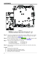
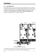
See 

Figure 1

 on Page 4.  The 

EN5004-0

#

 Communications Module pc board 

(

A12

) mounts to the left of the 

EN5002-00

 Main Control pcb (

A1

), with connector 

P13

 plugged into 

J13

.  Make sure all pins on the connector line up. 

Step 4 

Position the boards over the stand-offs.  Firmly push both boards onto the stand-offs 
until they are fully seated under the plastic clips.  Minimize pc board flexing by 
pushing directly on the areas surrounding stand-offs holes.  Check the front panel 
for proper alignment of indicating lights and push button switches. 


Summary of Contents for AT10.1 series

Page 1: ...Operating Instructions AT10 1 AT30SERIES MICROPROCESSOR CONTROLLED FLOAT BATTERY CHARGER COMMUNICATIONS MODULE DNP3 Level 2 Modbus Protocols JA0102 04...

Page 2: ...y standard modem and modem cable are also available Refer to the items listed below for part information and check off which items were supplied STANDARD COMMUNICATION MODULES Part No Communications M...

Page 3: ...ort LEDs 17 6 RESET Button 18 7 DNP V3 00 19 7 1 Introduction 19 7 2 Device Profile 19 7 3 Implementation Table 22 7 4 Point List 25 7 4 1 Binary Inputs 25 7 4 2 Binary Output Status Points 26 7 4 3 A...

Page 4: ...rminal Unit The advantage of ASCII allows less strict serial timing requirements without causing communication errors The advantage of RTU allows more data to be transmitted than ASCII mode for higher...

Page 5: ...arrier Installation Steps Step 1 Turn off the ac and dc circuit breakers on the AT charger Using a voltmeter verify that all potential voltages on the I O panel are zero This includes the dc output te...

Page 6: ...connect GROUND wire 244 to spade terminal next to connection plug J20 See assembly drawing JE5107 20 Step 7 Connect the serial communications connection a use TB11 for RS 232 see Section 3 2 1 b use T...

Page 7: ...s The communications option supports RS 232 and RS 485 RS 232 is a standard serial communication used on personal computers It has a limited cable distance and is susceptible to electrical noise RS 48...

Page 8: ...lines are disabled Disable the hardware handshaking lines by setting configuration switch S1 6 to the OFF position 8 TDX RDX COM CTS RTS 3 2 5 8 7 2 3 7 5 4 RS 232 PC Connection DB25 DB9 JUMPER NOT R...

Page 9: ...operation the hardware handshaking lines are enabled Enable the hardware handshaking lines by setting configuration switch S1 6 to the ON position 8 TDX RDX COM CTS RTS 3 2 5 8 7 2 3 7 5 4 RS 232 PC C...

Page 10: ...nation resistors requires a significantly lower value of biasing resistors which results in greater dc loading of the network Network design and biasing resistor calculations depend on the number of n...

Page 11: ...ble the terminating resistor The device communicating with the charger needs its own terminating resistor installed 8 5 POSITIVE NEGATIVE COMMON SHIELD RS 485 Single Connection Figure 5 RS 485 Single...

Page 12: ...of the network do not require the terminating resistor Move the jumper on J22 between pins 2 and 3 to disable the terminating resistor Figure 6 and Figure 7 show examples of multiple chargers on a RS...

Page 13: ...rop 3 Chargers Charger No 2 Charger No 1 Charger No 3 7 5 8 5 Figure 7 RS 485 Multi Drop 3 Chargers Typical RS 485 applications tie the shield to earth ground at only one 1 location along the network...

Page 14: ...of fiber connections compatible with standard B B and Dymec type converters Please refer to the following supplemental documentation for the available Fiber Optics Interface options EJ5230 04 http ww...

Page 15: ...e This modem will not work with office digital phone systems The telephone line needs to be a dedicated analog phone line similar to most fax machines Plug in the ac power supply The host software nee...

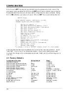
Page 16: ...1 Configuration Position Description ON position OFF position DIP S1 1 Setup Program Enabled Disabled DIP S1 2 Configuration Parameters User Values Factory Default Values DIP S1 3 Protocol DNP Modbus...

Page 17: ...168 1 100 10 Netmask 255 255 255 0 11 Gateway 0 0 0 0 12 Enable Modbus over TCP IP 0 disabled 13 Modbus TCP Port 502 14 Enable DNP over TCP IP 0 disabled 15 DNP TCP Port 20000 16 RESTART Comm Board To...

Page 18: ...NP TCP Port 20000 16 RESTART Comm Board To change a value or RESTART please select its item number After all parameters have been modified to the correct values turn off switch S1 1 Select RESTART Com...

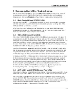
Page 19: ...s any time activity is detected on the network This activity may be messages to from other devices on the network In addition the flashing RXD LED only indicates that there are transitions on the netw...

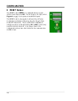
Page 20: ...of the RESET button The RESET switch when pushed will restart the AT Series Communication Module without resetting the charger s Main Control PC Board A1 This is useful when configuration changes are...

Page 21: ...hould provide a complete interoperability configuration guide for the AT Series Communications Module interface The Implementation Table provided in Section 7 3 on page 22 The Point List Tables provid...

Page 22: ...7 Fixed at 30000 ms if unsolicited messages is off Configurable if unsolicited messages is on See setup Unsolicited response notification delay 7 Fixed at 15000 ms Delay Measurement 100 ms Synchroniz...

Page 23: ...LICITED Function codes supported Sends Static Data in Unsolicited Responses 7 Never When Device Restarts When Status Flags Change No other options are permitted Default Counter Object Variation 7 No C...

Page 24: ...all 07 08 limited qty 17 28 index 129 response 00 01 start stop 17 28 index see note 2 1 2 Binary Input with Status 1 read 22 assign class 00 01 start stop 06 no range or all 07 08 limited qty 17 28 i...

Page 25: ...l 07 08 limited qty 129 response 130 unsol resp 17 28 index 34 0 Analog Input Reporting Deadband Variation 0 is used to request default variation 1 read 00 01 start stop 06 no range or all 07 08 limit...

Page 26: ...read 06 no range or all 07 08 limited qty 60 4 Class 3 Data 20 enbl unsol 21 dsbl unsol 22 assign class 06 no range or all No Object function code only see note 3 13 cold restart No Object function co...

Page 27: ...Event Class 1 2 3 or none 0 HVDC Alarm 1 active 1 1 LVDC Alarm 1 active 1 2 DC Output Failure Alarm 1 active 1 3 AC input Failure Alarm 1 active 1 4 Positive Ground Fault Alarm 1 active 1 5 Negative...

Page 28: ...operate 6 direct operate noack Point Index Name Description Methods 0 Equalize Mode Latch On Latch Off 0 float 1 equalize 1 Manual Timer Method Latch On 1 enabled 2 Manual Equalize Method Latch On 1 e...

Page 29: ...ble to all scaling possibilities The Default Deadband column is used to represent the absolute amount by which the point must change before an analog change event will be generated The Default Change...

Page 30: ...ction Codes supported 3 select 4 operate 5 direct operate 6 direct operate noack Point Index Name Description Scaling and Units representation of 32767 Valid Range 0 Float Voltage Setpoint 3276 7 Volt...

Page 31: ...ed Can be set at any time and does not indicate an error condition No 5 IIN1 5 Local mode Set if some points are uncontrollable via DNP No 6 IIN1 6 Device Trouble No 7 IIN1 7 Device restart Set only u...

Page 32: ...p n EJ5037 The Modbus protocol was implemented using the Modicon Modbus Protocol Reference Guide PI MBUS 300 Rev J 8 2 Supported Function Codes Below is the list of supported function codes 01 Read C...

Page 33: ...on one 1 of the equalize methods the charger will turn off the other two 2 equalize methods automatically 8 3 2 Binary Inputs Address Name Description 10001 HVDC High Voltage DC Alarm 10002 LVDC Low V...

Page 34: ...tery Temperature Temperature in Celsius 1 8 3 4 Holding Registers Address Name Description Multiplier 40001 Float Voltage Setpoint Float Voltage Setpoint 10 40002 Equalize Voltage Setpoint Equalize Vo...

Page 35: ...1 0 48 0 76 0 30 0 50 0 130 110 0 141 0 117 0 149 0 120 0 175 0 80 0 126 0 9 2 Current Ranges Current Limit Current Rating Amperes Min Max 6 3 0 6 6 12 6 0 13 2 16 8 0 17 6 20 10 0 22 0 25 12 5 27 5 3...

Page 36: ...from a remote location Meters Voltage Current Equalize Time Remaining Battery Temperature Setpoints Float Voltage Equalize Voltage Equalize Time Current Limit High DC Voltage Alarm Low DC Voltage Ala...

Page 37: ...or higher already support the AT Series Communications Module option How do you connect to the AT Communications Module The AT Communication Module supports a serial connection using RS 232 RS 485 or...

Page 38: ...will also need a modem The computer system will dial out to the AT Series charger The modem connected at the charger will answer the call and start communicating Refer to the special User Instruction...

Page 39: ...Module Operating Manual JD5008 00 http www ATSeries net PDFs JD5008 00 pdf AT Communications Module Field Installation JD5012 00 http www ATSeries net PDFs JD5012 00 pdf AT Main Ctrl PC Board A1 Field...

Page 40: ...the EN5004 0 Communications Module PC Board A12 may incur damage upon start up Charger Output 12 Vdc 24 Vdc 48 Vdc 130 Vdc Field Install Kit EJ5037 11 EJ5037 12 EJ5037 13 EJ5037 14 R29 Rating 11W 15 O...

Page 41: ...ct the new Ground Wire 7 Route the remaining wires 194 195 which end at the 4 pin Molex type plug along the charger s main signal harness The wires will lead to the left side of the Main Control PC Bo...

Page 42: ...awing itemized internal component layout electrical schematic with component ratings and a full connection diagram If the standard drawings featured in this manual are not sufficient please contact yo...

Page 43: ...Series net PDFs JD5010 00 pdf AT Power Res R3 Field Installation JD5012 00 http www ATSeries net PDFs JD5012 00 pdf Main Ctrl PC Board A1 Field Installation DC5016 00 http www ATSeries net PDFs DC5016...

Page 44: ...JA0102 04 TYPICAL APPLICATIONS FOR SCADA SYSTEMS http www atseries net PDFs JA0102 04 pdf JA0102 04 Rev 06 2021...

Reviews: