background image

78

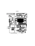
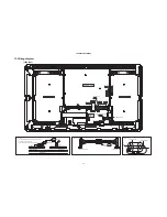
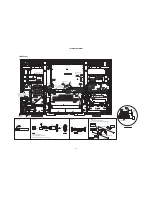
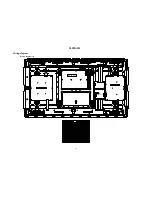
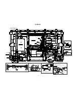
32PD5000/42PD5000

PAS4

PPU1

PANEL Y-SUS

POWER UNIT

SP TERMINAL R PWB

FILTER PWB

LABEL

POW SW

LED/RECEIVER PWB

PSW PPU2

PSC2

(*7)

CN61

No.22

No.19

CN63

EJP2

EJP1

P#GX00402

NVS8

Wind the wire by 1 turn.

P#2169512

Wind the wire by 1 turn.

P#2169513

NVS3

CNPPS

No.6

NVS2

No.24

No.15

EJF1

EJA1

No.12

EJF2

EJF5

EJF6

No.13
No.17

EJF3

NVS1

P#BZ10611

NVS9

PCV sheet

Pass the wire under PCV sheet.

No.27

#00W1 SK binder

Bundle the following wires:

Lead of AC INLET,

Lead of POW SW,

GND wire No.27.

No.7

(*8)

NVS10

P#2169513

Pay attention not to pinch the wire by rear cover.

ESW

#00W2 SK binder Fix the ferrite

core with the holder of panel module

after clamping.

P#2169511

No.5

(*4)

(*4)

EJF4

PANEL X-SUS

#00W3 SK binder Fix the

ferrite core with the holder

of bracket after clamping.

EAS2

EFJ1 EFJ4

EFJ2

EFA1 EFL1

EFK1

EFG1 EFG2

AUDIO PWB

EAJ1

No.14

FORMATTER UNIT

No.20

No.15

NVS4

(EJF4

EFJ4)

EAS1

No.21

No.16

SP TERMINAL L PWB

PAS3

ECONT

TACT SW PWB

No.18

EFM1

No.4

from panel module

NVS6 P#2168511

(*5)

EFJ3

(*9)

No.18

ECONT

TACT SW PWB

GND

L

N

1

2

E902

E901

E903

6

1

6

1

NVS10

Detail of (*5)

EJF3

No.14

NVS1

EJF3

To previous page

EAF1

Detail of (*7)

LABEL

black

white

Faston connector with Lock:

Connect it completely to be locked.

Disconnect it pushing the button to release the lock.

Detail of (*8)

(blue)
(orange)
(brown)

Detail of (*9)

Pass No.14 connector through NVS1.

Insert it in EJF3/EFJ3 and push the stopper down to lock.

50P Flat cable

stopper

blue band

electrode side

JOINT PWB

FORMATTER PWB

Flat core

P#GX00402

                                 [42PD5000]

Summary of Contents for 32PD5000

Page 1: ...nt Filter are made of glass handling the broken Module and Filter shall be taken care sufficiently in order not to be injured 2 Replacing work shall be started after the Panel Module and the AC DC Power Supply become sufficiently cool 3 Special care shall be taken to the display area in order not to damage its surface 4 The Panel Module shall not be touched with bare hand to protect its surface fr...

Page 2: ... You will die or take damage by electric shock if you touch to live part Use recommended components Please use to same characteristic compo nent which is same as previous for your safety and keep reliability especially marked by in parts list and circuit diagram It is reason of electric shock or fire if you use non recommended component Should be kept same style of wiring or component Monitor uses...

Page 3: ...onvergence and display distortion High Performance Digital Processor A wide range of personal computer signals can be handled from 640 x 400 640 x 480 VGA to 1600 x 1200 UXGA Easy to use remote control and on screen display system The remote control included eases the work of setting display controls Further the on screen display system displays the status of signal reception and display control s...

Page 4: ...display images free from color misconvergence and display distortion High Performance Digital Processor A wide range of personal computer signals can be handled from 640 x 400 640 x 480 VGA to 1600 x 1200 UXGA RGB analog input Easy to use remote control and on screen display system The remote control included eases the work of setting display controls Further the on screen display system displays ...

Page 5: ...l 2K Sync on green 0 3 Vp p 75 Video input Input signals Input terminals AV1 composite video input terminal RCA AV1 Y PB PR video input terminal RCA AV1 L R audio input terminal RCA AV2 composite video input terminal RCA AV2 Y G PB B PR R video input terminal RCA AV2 L R audio input terminal RCA AV3 composite video input terminal RCA AV3 S video input terminal RCA AV3 L R audio input terminal RCA ...

Page 6: ...deo input terminal RCA AV1 Y PB PR video input terminal RCA AV1 L R audio input terminal RCA AV2 composite video input terminal RCA AV2 Y G PB B PR R video input terminal RCA AV2 L R audio input terminal RCA AV3 composite video input terminal RCA AV3 S video input terminal RCA AV3 L R audio input terminal RCA AV4 composite video S video RGB L R audio input terminal Scart Video signals AV1 PAL SECA...

Page 7: ...7 55PMA550 2 Specifications 00E Applicable video signals for each input terminal Terminal RCA SCART DVI D sub Signal CVBS S video Component RGB PC STB RGB Component AV1 AV2 AV3 AV4 RGB1 RGB2 Available ...

Page 8: ...CT button INPUT SELECT button OK button RECALL button SELECT button SUB POWER button VOLUME UP DOWN buttons ADJUST buttons Main power switch Indicating lamp MENU button indicates the function while the MENU is displayed on the screen CLE 958 for 37PD5000TE CLE 952A for 37PD5000VE packed with AV3000E ...

Page 9: ...lder from soldered joints when replacing components If leaded solder should be added to existing lead free joints mix in the leaded solder thoroughly after the lead free solder has been completely melted do not apply the soldering iron without solder Servicing soldering iron A soldering iron with a temperature setting capability temperature control function is recommended The melting point of lead...

Page 10: ...PTION PARTS No DESCRIPTION 01SA 86994102 SCREW BT BIND HEAD 3X10 01SB1 4525404 SCREW M3X10 T 01SB2 4525404 SCREW M3X10 T 02SB3 4525401 SCREW M3X8 03SB4 4525404 SCREW M3X10 T 04SC 4525404 SCREW M3X10 T 05 QL23991 EXTEND LABEL VT 11 SG35204 CARTON BOX SG35207 CARTON BOX A11 JP06951 PWB ASS Y VIDEO A22 JP06961 PWB ASS Y TUNER A ETV1 2908801 CONNECTOR 8P ETV2 EK01108 WIRE PROCESSED 50P E04 EW08102 CAB...

Page 11: ...CREW M3X10 T 4525404 SCREW M3X10 T 05 QL23991 EXTEND LABEL VT QL23992 EXTEND LABEL V 06 SG35691 PAD PROTECTOR 08S SG34401 FRONT PAD SG34401 FRONT PAD 300 QJ01192 STAND ASS Y QJ01192 STAND ASS Y 641 4522885 SCREW 3X8 CE CP GRIP 790 MJ03041 BOLT M6X25 WITH WASHER MJ03041 BOLT M6X25 WITH WASHER A11 JP06951 PWB ASS Y VIDEO JP06951 PWB ASS Y VIDEO A22 JP06961 PWB ASS Y TUNER A ETV1 2908801 CONNECTOR 8P...

Page 12: ... H FREQ_2 I SYNC for H Frequency Detection Sub Picture 26 RESERVE NC 27 H FREQ_1 I SYNC for H Frequency Detection Main Picture 28 PDWN O RESERVE LVDS POWER DOWN MODE Panel Always High 29 SCL1 O IIC BUS CONTROL CLOCK TUNER PWB 30 SDA1 I O IIC BUS CONTROL DATA TUNER PWB 31 TXD1 O DATA RS 232C 32 RXD1 I DATA RS 232C 33 SCLK I CLOCK FLASH MEMORY Writing 34 BUSY O BUSY FLASH MEMORY Writing 35 TXD2 O RE...

Page 13: ...al M 4 3 H 16 9 69 TV AFC I AFC Voltage F E 70 FE AGC_I I AGC Voltage F E 71 RESERVE NC 72 FE MUTE NC 73 FE ST NC 74 FE SAP NC 75 FE MONO NC 76 FE MODE NC 77 RESERVE NC 78 RESERVE NC 79 SCL0 O IIC BUS CONTROL CLOCK VIDEO PWB 80 SDA0 I O IIC BUS CONTROL DATA VIDEO PWB 81 SCL3 O IIC BUS CONTROL CLOCK EEPROM 82 SDA3 I O IIC BUS CONTROL DATA EEPROM 83 MSP STATUS I MPX STATUS L Fixed H Changed 84 MSP R...

Page 14: ...2 MCV SYNC TA3IN P02 ENABLE SCL0 S 1 AD_KEY3 AN6 SDA0 S 2 S_DET_AV3 B2h 3Ah AD_KEY2 AN5 S 3 COMP_DET_AV2 RESET MSP_RESET FE AGC_I AN22 OSD CONTROLER S 4 COMP_DET_AV1 Sync Separator 80 81h Sync Separator FE AGC_O P21 OSDCM201 S2 2 TA1370FG TA1370FG TV AFC AN23 CLK4 SCLK S2 3 SCL0 SCL2 WSS AN24 SOUT4 SIN S2 3 SDA0 SDA2 AD_KEY1 AN4 P03 CS S2 4 CCD MAIN RESET RESET 90 91h D8 D9h Z86229 DC DDh H FREQ_2...

Page 15: ...selecting adjustment code buttons are used for changing data values OK button is used for confirming the data After finishing the necessary adjustment press MENU button Adjustment mode is released and the set returns to normal condition Memory Initialize operation NOTE The execution of this function returns the adjustment codes to the preset values therefore adjustment data will be lost Procedure ...

Page 16: ...N 15 8 8 31 SUB_CONTRAST AV1 MAIN SUB COMPOSITE mode 15 7 7 32 SUB_CONTRAST RF SUB 15 8 8 33 SUB_CONTRAST AV4 MAIN SUB COMPOSITE mode 15 7 7 34 SUB_COLOR VIDEO PAL SECAM MAIN 15 6 6 35 SUB_COLOR RF PAL SECAM MAIN 15 8 8 36 SUB_COLOR VIDEO NTSC MAIN 15 8 8 37 SUB_COLOR RF NTSC MAIN 15 6 6 38 SUB_COLOR VIDEO PAL SECAM SUB 15 8 8 39 SUB_COLOR RF PAL SECAM SUB 15 8 8 40 SUB_COLOR VIDEO NTSC SUB 15 8 8...

Page 17: ...C mode 15 9 9 137 DC_GAIN MAIN NTSC mode 15 6 6 138 VAP_GAIN MAIN NTSC mode 7 2 2 139 VAP_INV MAIN NTSC mode 31 10 10 140 YH_CORE MAIN NTSC mode 3 0 0 141 YHCGAIN MAIN NTSC mode 1 1 1 142 CDL MAIN NTSC mode 7 3 3 143 YNRK MAIN NTSC mode 1 1 1 144 YNRINV MAIN NTSC mode 1 0 0 145 YNRLIM MAIN NTSC mode 3 1 1 146 CNRK 1 1 1 147 CNRINV 1 0 0 148 CNRLIM 3 1 1 149 YPFG 15 10 10 150 SEPA_LEVEL 480i 576i 3...

Page 18: ...115 115 224 Tint Center CM NT3 HD1 HD2 HD5 PAL3 HD7 HD9 254 124 124 225 Center of Sharpness HV Enhancer Gain for Y For Europe TV 31 19 19 226 Center of Sharpness HV Enhancer Gain for Y For Europe VIDEO 31 18 18 227 Center of Sharpness HV Enhancer Gain for Y For Europe HD5 HD6 31 11 11 228 Center of Sharpness HV Enhancer Gain for Y For Europe HD1 HD4 HD7 HD8 31 7 7 229 Center of Sharpness HV Enhanc...

Page 19: ...7 127 307 Component Frq fH Setup 0 28 31 33 45KHz 1 28 31 45KHz 1 0 0 308 Terget value of White peak Adj Single Picture mode 237 235 235 309 Sharpness Gain S VIDEO Main 15 7 7 310 Sharpness Gain S VIDEO Sub 15 7 7 311 Select color control 0 Asia 1 South America Main Sub 1 0 0 312 Sharpness Gain Main N PAL 15 8 8 313 Sharpness f0 Main N PAL 3 2 2 314 Sharpness Gain Sub N PAL 15 9 9 315 Sharpness f0...

Page 20: ...Cinema 0 normal 1 Tele Cinema 412 V FREQ 60Hz Force 0 None 1 Yes Main Sub 1 0 0 413 COLOR SYSTEM CONTROL MODE 0 BW 2 3 58NTSC 3 4 43NTSC Main 414 COLOR SYSTEM CONTROL MODE 0 BW 2 3 58NTSC 3 4 43NTSC Sub 415 Horizontal Filter SW HHPF0 NTSC 1 0 0 416 Enhancer Gain HHPF1 PAL 1 0 0 417 Enhancer Gain HHPF2 HD 1 0 0 418 Horizontal Coring Level Enhancer Gain AS HECOR0_PO NT1 RF 15 1 419 Horizontal Coring...

Page 21: ... Vertical Enhancer Clip for Y G 0 LTI YVECLP0_P0 NTSC PAL Multi picture 1 1 487 YVECLP1_P0 HD 1 1 488 Vertical Clip Offset Level YVECLP0_P0 NTSC PAL Multi picture 15 7 489 YVECLP1_P0 HD 15 1 490 Vertical Non Linear Peaking for Y G YVNLP0_P0 NTSC PAL Multi picture 63 0 491 YVNLP1_P0 HD 63 0 492 Horizontal HPF Peak Freq SW for Y G YHHPF0_P0 NTSC PAL Multi picture 3 2 493 YHHPF1_P0 HD2 HD3 HD9 HD10 3...

Page 22: ...7 CHDSBC1 HD 7 0 0 578 Horizontal Enhancer Clip for B Y B R Y R 0 CTI CHECLP0 NTSC PAL Multi picture 1 0 0 579 CHECLP1 HD 1 0 0 580 Coring Amplitude for B Y B R Y R CC0R0 NTSC PAL Multi picture 7 1 1 581 CC0R1 HD 7 1 1 582 B Y Clamp offset Except D Sub Component NT1 2 3 HD2 3 PAL1 2 3 HD9 10 255 128 128 583 R Y Clamp offset Except D Sub Component NT1 2 3 HD2 3 PAL1 2 3 HD9 10 255 128 128 584 B Y C...

Page 23: ...harpness HV Enhance Gain for Y DVI STB VGA 31 2 2 666 DVI STB Setup 0 None VGA Others Yes 1 All none 2 All have DVI STB mode 2 0 0 667 HSYNC De Jitter 0 Low Disabled 1 High Enabled DVI PC 1 0 0 668 HSYNC De Jitter 0 Low Disabled 1 High Enabled DVI STB 1 0 0 669 HSYNC De Jitter 0 Low Disabled 1 High Enabled AVC 1 0 0 670 Horizontal Clip Offset Level for Y G AS YHECLPL3_P0 NT2 4 PAL2 4 15 10 671 EU ...

Page 24: ... of Component TV NTSC HD PC PC signal Video Input System Judgment of H Frequency Video Input Setup Mode AV1 AV2 PAL 15 75kHz 576i Auto PAL2 SDTV DVD PAL2 HDTV PAL3 NTSC 15 75kHz 480i Auto NT2 SDTV DVD NT2 HDTV NT3 PAL 31 25kHz 576p Auto HD10 SDTV DVD HD10 HDTV HD9 NTSC 31 50kHz 480p Auto HD3 SDTV DVD HD3 HDTV HD2 NTSC 45 00kHz 720p Auto HD5 SDTV DVD HD6 HDTV HD5 PAL 28 125kHz 1080i Auto HD7 SDTV D...

Page 25: ...Va test point and the GND point on the Power Supply Unit 2 If the difference between the printed voltage of Va and the indicated value of Va Voltmeter is over 0 2V adjust the Va ADJ VR located upward on the Power Supply Unit to make it within 0 2V 3 Receive the all black signal with no setup 3 Check and do the procedure 1 again 4 Check the indication of Vs and Va voltages printed on the label loca...

Page 26: ...26 55PMA550 55HDM71 PW1 00E ...

Page 27: ... AGC Adjustment and No 291 AGC Input 2 Receive the adjustment signal at ANT terminal Signal condition CCIR ch 5 175 25MHz PAL B G Philips Pattern Input Field Strength 50dBm 2 Increase the data of No 289 until the data of No 291 converges This is the point of AGC MAX 3 Decrease the data of No 289 until the data of No 291 diminishes and then press the OK button AGC POINT AGC Voltage AGC Max AGC Adj ...

Page 28: ...PD5200 55PMA550E Preparation Procedure 1 Input the adjustment signal of 576p or 480p format into AV1 input terminal 1 Select AV1 and enter the service adjustment mode the adjustment signal 2 Select No 700 RGB Amp Gain ADJ and press OK button for more than 2 seconds to start the adjustment It will complete the adjustment after the OSD of AUTO MODE disappeared 3 Select No 701 RGB Amp Gain ADJ and pr...

Page 29: ...by re adjustment in the specified way Item AUTOMATIC SIGNAL LEVEL ADJUSTMENT TV Applicable Model 42PD5200 32PD5200 37PD5200 55PMA550E Preparation Procedure 1 Input the adjustment signal modulated to RF frequency into ANT terminal 1 Select TV channel of the adjustment signal and enter the service adjustment mode the adjustment signal 2 Select No 702 Automatic White peak Adj Single and press OK butt...

Page 30: ...justment mode and confirm that No 3 R 4 G and 5 B are all 255 If the some data are not set to 255 4 Adjust the color temperature by way that reduces the one or two data in No 3 4 or 5 Note At least one of them should be 255 after adjustment Specification Color Temperature Normal for Video 9300K x 0 285 0 005 y 0 293 0 005 Adjustment of Warm mode 5 Enter the service adjustment mode and confirm that...

Page 31: ...31 55PMA550 55HDM71 PW1 00E ...

Page 32: ...ent mode and confirm that No 3 R 4 G and 5 B are all 255 If the some data are not set to 255 4 Adjust the color temperature by way that reduces the one or two data in No 3 4 or 5 Note At least one of them should be 255 after adjustment Specification Color Temperature Normal for Video 9300K x 0 285 0 005 y 0 293 0 005 Adjustment of Warm mode 5 Enter the service adjustment mode and confirm that No 6...

Page 33: ...two data in No 12 13 or 14 Note At least one of them should be 255 after adjustment Specification Color Temperature Cool for PC 12000K x 0 268 0 005 y 0 283 0 005 3 Set the display area to Full Adjustment of Normal Warm Black White mode This item must be done after the same adjustment for VIDEO mode 3 Set the adjusted value of COLOR TEMP ADJ VIDEO Normal Warm Black White mode Adj No 3 4 5 6 7 8 9 ...

Page 34: ...olor Temperature Cool for Video 12000K x 0 268 0 005 y 0 283 0 005 3 Set the display size to Full Adjustment of Normal mode This item must be done before the same adjustment for PC mode 3 Enter the service adjustment mode and confirm that No 3 R 4 G and 5 B are all 255 If the some data are not set to 255 4 Adjust the color temperature by way that reduces the one or two data in No 3 4 or 5 Note At ...

Page 35: ...re Cool for Video 12000K x 0 268 0 005 y 0 283 0 005 3 Set the display size to Full Adjustment of Normal mode This item must be done before the color temperature adjustment for PC mode 3 Enter the service adjustment mode and confirm that No 3 R 4 G and 5 B are all 255 If the some data are not set to 255 4 Adjust the color temperature by way that reduces the one or two data in No 3 4 or 5 Note At l...

Page 36: ...Adjust the color temperature by way that reduces the one or two data in No 12 13 or 14 Note At least one of them should be 255 after adjustment Specification Color Temperature Cool for PC 12000K x 0 268 0 005 y 0 283 0 005 3 Set the display area to Full Adjustment of Normal Warm Black White mode This item must be done after the same adjustment for VIDEO mode 3 Set the adjusted value of COLOR TEMP ...

Page 37: ...functions can recover by below method Press the SUB POWER button INPUT SELECT button and button at the same time and hold for more than 5 seconds The set turns on the service menu mode Select No 175 and data set from 0 to 1 Or Press the SUB POWER button and button at the same time and hold for more than 5 seconds Forced AVC mode only for 37PD5200 This model is set to Forced AVC mode It makes the s...

Page 38: ... PWB or Video PWB No Yes Power cannot be turned on LED does not light Is the input voltage applied to Power supply unit CN61 AC inlet Power switch AC Fuse F901 T6 3AH 250V Are the voltages applied to CN63 pins and CNPPS pins of Power supply unit CN63 5V CNPPS 30V 3 3V 5V 12V 10V Joint Formatter PWB Power supply unit No Yes Filter PWB L ch R ch GND Check Speaker terminal and Speaker cord Unlocked C...

Page 39: ...t correct Panel Module Panel Module Power supply unit Is the LED red or green orange Picture is not displayed LED is lighting Is Voltage applied to CN63 pin of the Power supply unit Power supply unit No 5V Yes Is Voltage applied to EJF1 pin of the Joint PWB Joint PWB Is the voltage of CN68 pin on the Power supply unit 5V Power supply unit Is it the power saving mode Formatter PWB Input signal Cabl...

Page 40: ...Input terminal Are waveforms at pin44 Y and 43 C of I501 Check I202 Check Q508 Q509 and Q510 Are waveforms at pin9 Y 11 CB and 13 CR of I202 PAL SECAM Are waveforms at pin21 Y 22 CB and 23 CR of I501 NTSC Are waveforms at pin5 Y and 7 C of I501 Yes Yes Yes Yes Yes No No No No No Check Q203 Q301 Q307 etc Check Q322 Q327 X304 or X305 etc Check I301 Yes Yes No Check Q317 Q324 Q328 X302 or X303 etc Ar...

Page 41: ...Q214 Q215 etc No Component Input RF TV Video Input Are waveforms at pin9 Y 11 CB and 13 CR of I202 Are waveforms at pin45 Y 47 CB and 1 CR of I202 Check I202 Check Input terminal No No Yes Yes No Are waveforms at pin21 Y 22 CB and 23 CR of I502 Check Q511 Q512 and Q513 Yes No Are waveforms at pin1 of I502 Check I502 Yes No Are waveforms at pin53 of I201 Check Q202 etc Yes No Check I201 U101 etc ...

Page 42: ...aveform at pin 16 H and 28 V of I601 Yes Yes No No Single picture or Main picture Sub picture Trouble of Sub picture Are waveforms at pin3 H and pin4 V of I601 No Check I601 Check I602 Are waveforms at pin24 of I601 Check Q601 Q603 Q609 Q610 etc Are waveforms at pin9 H and pin4 V of I501 Check I501 etc Yes Yes Yes No No Component Input without 480i 576i RF TV Video Input Component 480i 576i ...

Page 43: ... V of I601 Are waveforms at pin 19 H and 29 V of I601 Yes Yes No No No Check I601 Check I602 Are waveforms at pin26 of I601 Check Q606 Q608 Q609 Q610 etc Are waveforms at pin9 H and pin4 V of I502 Check I502 etc Yes Yes Yes No No Component Input without 480i 576i RF TV Video Input Component 480i 576i Trouble of Sub picture ...

Page 44: ... Video PWB Is waveform of pin 18 of U101 TV CV Yes Yes Check U101 No Check around Q101 Q102 Q103 No Picture of TV Is waveform of pin 30 31 of IN01 L R Is waveform of pin 2 of IN01 SIF Check around IN01 Yes No No Check PTV2 connector or Video PWB Yes Yes Check U101 No Check around QN01 QN02 No Sound of TV Asia Is waveform of pin 22 of U101 SIF Europe Is waveform of pin 21 of U101 SIF Asia ...

Page 45: ...Are waveforms of pin 32 33 34 of IT01 TEXT Check QT03 QT04 QT05 Yes No No Check PTV2 connector or Video PWB Is waveform of CT01 TV CV Yes Yes Check Video PWB No Check around QT01 QT02 No Teletext Is waveform of pin 23 of IT01 TV CV Check around IT01 No Yes ...

Page 46: ...SUB POWER button of the monitor or the remote control Procedure 1 Press the SUB POWER button and button on the bottom of the monitor at the same time and keep it for more than 5 seconds after the power turned on 2 It generates red blinking series of the power indicator light 3 Any operation would cancel the Self Diagnosis mode 4 The next table shows the PDP PWB in which failure most probably would...

Page 47: ...ched up Latest error code Self Check H11 OK H15 OK H16 OK H31 OK H32 OK H33 OK F63 F63 Self check result area Failure history area Check result Check item OSD Signal circuit self diagnosis function This function is for the failure of the signal circuit for example the phenomenon as below Sometimes power turns off abnormally Sometimes picture disappears abnormally To enter to this Self Diagnosis mo...

Page 48: ... PIN PYS SY 1 PIN PYM MPB 3 PIN PYS SPB 3 PIN PYS SPR 5 PIN PYM MPR 5 PIN TP01 MH 5 0Vp p TP03 SH TP04 SV TP02 MV 1V 1H 0 286Vp p 1H 2Vp p 1H 1 0Vp p 1H 1 4Vp p 1H 1 2Vp p 1H 1H 1 2Vp p 1H 5 0Vp p 0 3Vp p FILTER SW SP TERMINAL L SP TERMINAL R LED RECEIVER TACT SW board 49 AUDIO board 52 JOINT board 54 VIDEO board 1 55 VIDEO board 2 56 TUNER board 58 Basic circuit diagram list ...

Page 49: ...32PD5000 42PD5000 49 ...

Page 50: ...37P D5 00 0 50 ...

Page 51: ...55PMA550 51 ...

Page 52: ...32PD5000 42PD5000 52 ...

Page 53: ...55PMA550 55HDM71 53 ...

Page 54: ...32PD5000 42PD5000 54 ...

Page 55: ...32PD5000 42PD5000 55 ...

Page 56: ...32PD5000 42PD5000 56 ...

Page 57: ...55PMA550 55HDM71 57 ...

Page 58: ...32PD5000 42PD5000 58 ...

Page 59: ...55PMA550 55HDM71 59 ...

Page 60: ...FILTER board SW board TACT SW board SP TERMINAL R board LED RECEIVER board SP TERMINAL L board 32PD5000 42PD5000 9 Printed wiring board diagram 60 ...

Page 61: ...55PMA550 55HDM71 FILTER board SW board TACT SW board LED RECEIVER board SPEAKER TERMINAL R board SPEAKER TERMINAL L board 61 Printed wiring board diagram ...

Page 62: ...03 B2 EAF1 F3 Q408 B2 IC401 E2 IC402 C1 Cir No Position Cir No Position D401 D3 D412 D3 D402 D4 K405 E4 D403 D3 K410 E4 D404 D3 Q404 D2 D405 B3 Q405 D2 D408 D4 Q407 B2 D409 D3 D411 D3 AUDIO board side A AUDIO board side B Mainly chip parts reference table Mainly chip parts reference table 32PD5000 42PD5000 62 ...

Page 63: ... board side B Cir No Position Cir No Position DH98 A4 IF08 F4 DH99 A4 KH101 B5 EJF1 E5 KH102 A5 EJF2 F5 LH101 D5 EJF3 G2 LH101A D5 EJF4 C3 PCL1 G3 EJF5 G4 PTEM1 A5 EJF6 G3 Mainly chip parts reference table 32PD5000 42PD5000 63 ...

Page 64: ...3 L202 C6 L218 C3 L502 H2 Q210 D5 I301 K4 L203 D6 L219 A2 L503 G3 Q211 C5 I302 I4 L204 E6 L222 A5 L504 H4 Q212 D5 I303 K4 L205 G6 L301 I6 L507 G5 Q213 C5 I304 J4 L206 H6 L304 L4 L601 C2 Q214 B3 I305 J3 L207 G6 L306 L4 L602 D5 Q215 B3 I306 J5 L208 H6 L307 K4 L603 E4 Q301 I5 I307 K4 L209 I6 L308 L3 L604 F4 Q302 J5 I501 G3 L210 J6 L310 K4 PTV2 J1 I502 G4 L211 J6 L312 J3 Q202 C4 I601 E4 L212 J6 L313 J...

Page 65: ...Mainly chip parts reference table VIDEO board side B Cir No Position Cir No Position D301 J3 Q217 C4 D302 J3 Q325 K3 I001 B4 Q330 G4 I002 B5 Q515 G2 I203 A4 Q516 G4 Q001 B4 32PD5000 42PD5000 65 ...

Page 66: ...C5 Q104 F2 QN01 D5 I102 B5 LN01 E4 Q105 E2 QN02 D5 IC01 B5 LN02 D4 Q106 D2 QT01 B2 IC02 D5 LN03 E3 Q107 D2 QT02 B1 IC03 C4 LT01 C3 Q108 F5 QT03 B3 IN01 E3 LT02 A4 Q109 E5 QT04 B3 IT02 C1 PTV2 D6 QC01 D4 QT05 B3 L102 F3 Q101 F3 QC02 D5 QT06 C3 L104 D3 Q102 F2 QC03 B4 LC01 B4 Q103 E2 QC04 C4 TUNER board Side A TUNER board Side B 66 ...

Page 67: ...67 32PD5000 42PD5000 11 Block diagram ...

Page 68: ...68 55PMA550E Block diagram ...

Page 69: ...PWB CPU Sub CPU Main SPRLY MUTE SCL2 SDA2 Lch IN Rch IN IC401 NJW1136 MASTER VOL BALANCE BASS TREBLE CONT SURR ON OFF IC402 NJM2192AM TRUBASS MUTE RELAY IC404 TA2021B DIGITAL POWER AMP 12V I403 BU4052 TRUBASS CONT AUDIO PWB MUTE DRIVE RELAY DRIVE LED OFF RELAY MUTE SP OUT Lch SP OUT Rch 12V 12V LED OFF DTC PW1 CHASSIS CIRCUIT BLOCK DIAGRAM MAIN L R MAIN Y PB PR SUB HD VD MAIN HD VD SUB Y PB PR Y S...

Page 70: ...D VD MAIN HD VD SUB Y PB PR X Sustain Circuit Y Sustain Circuit Address Driver Scan Driver Driver Controller LVDS Receiver Signal Controller Data Controller Scan Driver RGB2 D sub 15 RGB1 DVI D RGB2 Audio IN RGB1 Audio IN SPRLY MUTE SCL2 SDA2 Lch IN Rch IN IC401 NJW1136 IC402 NJM2192AM MUTE RELAY IC404 TA2021B 12V I403 BU4052 MUTE DRIVE RELAY DRIVE LED OFF RELAY MUTE SP OUT Lch SP OUT Rch 12V 12V ...

Page 71: ... B6B PH CN68 B6B PH CN7 ZIF 20P CN69 20FMN BT 1 2 NC NC 3 4 NC GND NC 5 GND GND 6 7 8 9 10 Vsago Vcego PFCgo GND GND GND GND 11 12 13 14 15 16 17 18 19 20 Vra Vrs NC GND NC NC 1 2 3 4 5 6 7 8 9 10 11 12 13 14 15 16 17 18 19 20 NC NC NC GND NC GND GND VSAGO VCEGO PFCGO GND GND GND GND Vra Vrs NC GND NC NC POWER UNIT 1 2 RA GND LVDS 3 4 RA RB SCL 5 RB RC RC RCLK RCLK RD 6 7 8 9 10 11 12 13 14 15 16 ...

Page 72: ...72 55PMA550 12 Connection diagram PW1 55V CONNECTION DIAGRAM ...

Page 73: ...S5 To next page NVS5 P 2169512 Detail of 1 1 Release the lock of CN7 and insert No 3 connector in CN7 2 Lock CN7 to fix the inserted No 3 3 Insert the other side of No 3 in CN69 completely Detail of 4 PANEL LOGIC PWB POWER UNIT CN69 3 2 1 CN7 No 3 printed letters side PANEL MODULE 20PFFC CN1 To PANEL LOGIC PWB No 4 Detail of 3 CONNECTOR WIRE FERRITE CORE EFM1 To FORMATTER PWB 13 Wiring diagram 32P...

Page 74: ...P 2169513 EAS2 EAS1 PAS3 EFK1 EJF4 No 24 No 18 purse lock No 13 No 16 ECONT EJF3 NVS1 P BZ10611 EFM1 No 11 E903 Pass it under the wire from AC INLET PSW No 17 NVS8 P GX00402 No 25 4 No 10 EJA1 EJF1 EJP1 EJP2 EJF2 EJF5 4 NVS3 Wind the wire by 1 turn P 2169512 CNPPS No 6 EJF6 EAF1 EAJ1 CN63 No 5 No 15 purse lock TACT SW PWB P GX00402 NVS4 No 12 EFJ3 8 EFJ2 EFJ1 EFJ4 EFA1 EFL1 EFG1 EFG2 00W1 purse Lo...

Page 75: ...r in CN7 2 Lock CN7 to fix the inserted No 3 3 Insert the other side of No 3 in CN69 completely Detail of 4 PANEL LOGIC PWB POWER UNIT CN69 3 2 1 CN7 No 3 printed letters side PANEL MODULE 20PFFC CN1 To PANEL LOGIC PWB No 4 Detail of 3 CONNECTOR WIRE FERRITE CORE EFM1 To FORMATTER PWB POWER UNIT PANEL Y SUS To next page PANEL X SUS PANEL ABUS R To FORMATTER PWB PANEL ABUS L PANEL LOGIC ...

Page 76: ...n Black White Detail of 8 Pass No 12 connector through NVS1 Insert it in EJF3 EFJ3 and push the stopper down to lock 50P Flat cable stopper blue band electrode side JOINT PWB FORMATTER PWB Flat core PPU1 CN61 Detail of 6 Faston connector with Lock Connect it completely to be locked Disconnect it pushing the button to release the lock GND L N 2 1 black white E901 SUP C14608 A view B view LABEL E902...

Page 77: ...77 32PD5000 42PD5000 42PD5000 ...

Page 78: ...g P 2169511 No 5 4 4 EJF4 PANEL X SUS 00W3 SK binder Fix the ferrite core with the holder of bracket after clamping EAS2 EFJ1 EFJ4 EFJ2 EFA1 EFL1 EFK1 EFG1 EFG2 AUDIO PWB EAJ1 No 14 FORMATTER UNIT No 20 No 15 NVS4 EJF4 EFJ4 EAS1 No 21 No 16 SPTERMINALLPWB PAS3 ECONT TACT SW PWB No 18 EFM1 No 4 from panel module NVS6 P 2168511 5 EFJ3 9 No 18 ECONT TACT SW PWB GND L N 1 2 E902 E901 E903 6 1 6 1 NVS1...

Page 79: ...79 55PMA550 Wiring diagram Wiring diagram 1 2 ...

Page 80: ...80 55PMA550 Wiring diagram 2 2 ...

Page 81: ... X SUS PWB Ass y FPF20R XSS0001 4 Y SUS PWB Ass y FPF20R YSS0002 5 A BUS L PWB Ass y FPF20R ABL0003 6 A BUS R PWB Ass y FPF20R ABR0004 PANEL Y SUS PANEL X SUS PANEL ABUS L PANEL ABUS R PANEL LOGIC 4 5 2 6 3 Attachment for packing Apply it before packing this panel module Handle for packing Apply it before packing this panel module Attachment for packing Apply it before packing this panel module Ha...

Page 82: ...Panel Module 32V The assembled form in a product before servcing PANEL Y SUS PANEL X SUS PANEL ABUS L PANEL ABUS R PANEL LOGIC Panel Holder x2 Remove these holders and apply the handles attachments for packing Handle Handle ...

Page 83: ...83 32PD5000 42PD5000 42PD5000 ...

Page 84: ...84 37PD5200 37PD5000 ...

Page 85: ...85 55PMA550 14 Disassembly diagram ...

Page 86: ...FHP Panel Module 42V Rear view The state of a panel simple substance No Spare Part Name FHP Spare Part 1 Panel Module FPF42C128128UC 55 2 LOGIC PWB Ass y FPF23R LGC0005 A1 ASIC 3 X SUS PWB Ass y FPF23R XSS0005 4 Y SUS PWB Ass y FPF23R YSS0006 5 A BUS L PWB Ass y FPF23R ABL0001 6 A BUS R PWB Ass y FPF23R ABR0002 PANEL Y SUS PANEL X SUS PANEL LOGIC PANEL ABUS L PANEL ABUS R Attachment for packing x8...

Page 87: ...e for packing Apply it before packing this panel module Attachment for packing Apply it before packing this panel module Handle for packing Apply it before packing this panel module 㧔 ޓޓޓޓޓޓޓ 㧕 LOGIC PWB ASS Y Manufactured at FHP factory X SUS PWB ASS Y Manufactured at FHP factory R ADR PWB ASS Y Manufactured at FHP factory L ADR PWB ASS Y Manufactured at FHP factory 2 3 4 5 6 No 1 2 3 4 5 6 Spare...

Page 88: ...NEL Y SUS PANEL X SUS PANEL ABUS R PANEL ABUS L PANEL LOGIC Panel Module 37V The assembled form in a product before servicing Handle Handle Panel Holder x2 Remove these holders and apply the handles attachments for packing ...

Page 89: ...89 55PMA550 ...

Page 90: ......

Page 91: ...THE UPDATED PARTS LIST FOR THIS MODEL IS AVAILABLE ON ESTA ...

Page 92: ...HITACHI SM005 Power Supply Block Diagram 92 ...

Page 93: ...HITACHI SM005 Panel Connectors 93 ...

Page 94: ...HITACHI SM005 Power Supply Circuit Board ...

Page 95: ...HITACHI SM005 Power Supply Circuit 1 of 5 ...

Page 96: ...HITACHI SM005 Power Supply Circuit 2 of 5 ...

Page 97: ...HITACHI SM005 Power Supply Circuit 3 of 5 ...

Page 98: ...HITACHI SM005 Power Supply Circuit 4 of 5 ...

Page 99: ...HITACHI SM005 Power Supply Circuit 5 of 5 ...

Page 100: ...005 D008 R L001 P C003 Q010 etc NO Vs Va Vcc open connector CN64 impedance check Vs LINE impedance check Vs LINE P DP module Vs NG impedance check Va LINE open connector CN64 impedance check Va LINE P DP module Va NG D351 D551 D550 Va no uprise Vs down after up Vs no uprise Va down after up S W ON Q303 P C301 P C302 D310 IC391 etc IC391 Q501 IC501 D510 Q502 P C501 P C502 D235 D236 etc NO Vs Va Vcc...

Page 101: ...47 Milano Italia ITALY Tel 39 02 487861 Tel 39 02 38073415 Servizio Clienti Fax 39 02 48786381 2 Email customerservice italy hitachi eu com HITACHI Europe AB Box 77 S 164 94 Kista SWEDEN Tel 46 0 8 562 711 00 Fax 46 0 8 562 711 13 Email csgswe hitachi eu com HITACHI EUROPE S A S Lyon Office B P 45 69671 BRON CEDEX FRANCE Tel 04 72 14 29 70 Fax 04 72 14 29 99 Email france consommateur hitachi eu co...

Reviews: