62
DP33KA/B
3 5
5 3
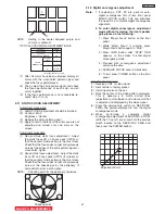
Top and bottom of the circle is between
outer edge and inner edge.
Outer edge of the circle
Inner edge of the circle
H size marker
0.7~1.5
H size marker
0.7~1.5
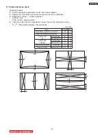
2.18 Scanning area check
Checking condition
(1) Digital convergence adjustment should have
been completed.
(2) Receive the circle pattern signal.
(3) Brightness/Contrast - standard condition
Contrast:max
Other controls:center position
(4) Check that the scanning area matches with the
following drawing.
2.17 Horizontal position adjustment
Adjustment preparation
(1) The screen face of set should be turned to East
or West.
(2) VIDEO control should be set to Factory Preset
Condition.
(3) DIGITAL CONVERGENCE adjustment should
be finished.
Adjustment procedure
NORMAL 16:9 STANDARD MODE
(1) Receive circle pattern.
(2) Picture Format is 16:9 Standard.
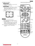
(3) Go to I
2
C Adj. mode by pressing INPUT and
POWER button on control panel at the same
time.
(4) Choose H. POSITION item using R/C CURSOR
G
,
H
.
(5) Adjust HORIZONTAL POSITION as follows,
using R/C CURSOR
F
,
E
.
Spec: Balance Left/Right side display position.
H. size marker 1.0~2.0.
Adjustment procedure
1080i 16:9 Standard Mode
(1) Input 1080i (fH=33.75KHz) component circle
pattern signal to component video terminal.
(2) Picture Format is 16:9 Standard.
(3) Go to I
2
C Adj. mode.
(4) Choose H. POSITION item using R/C CURSOR
G
,
H
.
(5) Adjust HORIZONTAL POSITION as follows,
using R/C CURSOR
F
,
E
.
Spec: Balance Left/Right side display position.
BACK TO ADJUSTMENTS
Summary of Contents for 46F500A
Page 28: ...28 DP33KA B a Adjust Mode OSD continued ...
Page 29: ...29 DP33KA B a Adjust Mode OSD continued ...
Page 30: ...30 DP33KA B a Adjust Mode OSD continued ...
Page 56: ...56 DP33KA B Convergence For Outside Signal function ...
Page 111: ...PRINTED CIRCUIT BOARD SIGNAL P W B PART SIDE 111 DP33KA B TABLE OF CONTENTS ...
Page 112: ...DP33KA B PRINTED CIRCUIT BOARD SIGNAL P W B PATTERN SIDE 112 ...
Page 113: ...PRINTED CIRCUIT BOARD TERMINAL P W B PART SIDE 113 DP33KA B ...
Page 114: ...PRINTED CIRCUIT BOARD TERMINAL P W B PATTERN SIDE 114 DP33KA B ...
Page 115: ...DP33KA B PRINTED CIRCUIT BOARD POWER P W B PART SIDE 115 ...
Page 116: ...PRINTED CIRCUIT BOARD POWER P W B PATTERN SIDE 116 DP33KA B ...
Page 117: ...DP33KA B PRINTED CIRCUIT BOARD DEFLECTION P W B PART SIDE 117 ...
Page 118: ...PRINTED CIRCUIT BOARD DEFLECTION P W B PATTERN SIDE 118 DP33KA B ...
Page 119: ...DP33KA B PRINTED CIRCUIT BOARD CPT P W B PART SIDE 46F500A 119 ...
Page 120: ...PRINTED CIRCUIT BOARD CPT P W B PATTERN SIDE 120 DP33KA B ...
Page 121: ...PRINTED CIRCUIT BOARD 46F510 CONTROL P W B 121 DP33KA B ...
Page 122: ...DP33KA B PRINTED CIRCUIT BOARD DVI P W B PART SIDE 122 ...
Page 123: ...PRINTED CIRCUIT BOARD DVI P W B PATTERN SIDE 123 DP33KA B ...
Page 124: ...BLOCK DIAGRAM 124 DP33KA B TABLE OF CONTENTS ...
Page 125: ...125 DP33KA B WIRING DIAGRAM TABLE OF CONTENTS ...
Page 162: ......


