DP-3X SW +115V POWER SUPPLY REGULATION EXPLANATION
PAGE 01-13
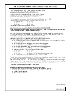
Hi-Voltage Power Supply Circuit Diagram explanation:
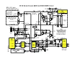
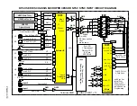
(See Power Supply SW+115V Regulation Circuit Diagram for details)
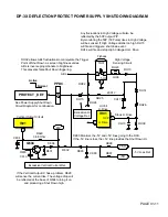
THIS POWER SUPPLY RUNS ONLY WHEN THE SET IS TURNED ON:
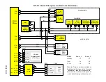
TURNING ON THE SW +115V POWER SUPPLY:
When the Set is turned on, the Microprocessor
I001
Outputs a Power On/Off 1 high command via pin
59
. This
Power On command is routed through
Q027
and
Q028
to the
PPS4
connector pin
7
. This High will be passed to
the base of
Q902
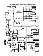
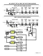
provided the Shut Down sensor
Q904
isn’t activated. When the base of
Q902
goes high, it’s
collector will go low. This will supply a ground path for the power on Relay
S901
turning it on. When the relay is
energized, AC is supplied to the Bridge rectifier
D901
.
D901
develops raw 150V which is routed through
F903
to Pins
1
and
2
of
T901
. This voltage is routed through
the primary coil inside
T901
and out pins
5
and
6
to pin
3
of
I901
which is the Drain of the internal Switch MOS
FET. The Ground return path for the primary voltage is out pin
2
of
I901
which is the Source of the internal
Switch MOS FET and then through four 0.22 ohm resistors
R908
,
R909
,
R910
and
R911
.
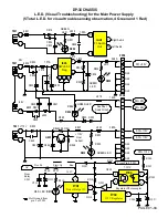
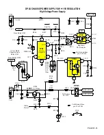
See SW+115V Regulation Circuit Diagram for details.
SW +115 REGULATION
SW +115V pulse is generated from pin
11
of
T901
. This pulse is rectified by
D925
, filtered by
C943
and then
routed through the Excessive Current sensing circuit
R944
and
Q905
.
The primary route for the
SW +115V
is through
E907
,
L923
to pin
9
and
10
of
PPD5
and output as
SW +115V
to the Deflection circuit and High Voltage generation circuit.
However, the regulation route is through
E906
to pin
1
of
I904
. Internally, the regulator transistor works as a
variable resistor whose resistance is dependant upon the
SW +115V
voltage fluctuations. The internal variable
resistor manipulates the current flow from pin
2
to pin
3
ground. This will cause the voltage at pin
2
of
I903
to be
manipulated. Internally, the LED is illuminated by degrees dependant upon the
SW +115V
voltage fluctuations.
The internal receiver receives this light and acts as a variable resistor from pin
4
to pin
3
which is the regulation
control signal.
This action causes pin
1
of
I901
to manipulate the internal oscillator within
I901
. This in turn causes the fre-
quency of the drive pulse delivered to the Gate of the internal SMOSFET (Switch Metal Oxide Semiconductor
Field Effect Transistor) to manipulate the frequency of the pulse generated on the primary of
T901
. The current
drain of the internal SMOSFET is monitored by four low ohm resistors mentioned above. If this current exceeds
a specific value, the voltage developed by these low ohm resistors is routed through
R912
back into pin
1
which
is the Over Current Protection circuit as well as the Regulation Control pin. This pin will inhibit the drive signal
to the gate of the SMOSFET. As soon as the excessive current situation is eliminated, the IC will recover and
continue functioning.
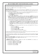
B+ GENERATION FOR THE POWER SUPPLY DRIVER IC:
Vcc for the Driver IC is first generated by the AC input. This voltage is called Start Up Voltage.
I901
requires
23.3V
DC to operate normal. However, it will begin operation at
12V DC
on pin
4
of
I901
.
When AC is applied to the main full wave bridge rectifier
D901
where it is converted to Raw 150V DC voltage
to be supplied to the power supply switching transformer
T901
pin
1
and
2
.
However, one leg of the AC is routed to a half wave filter consisting of
R906
and
R907
(both a 3.9K ohm resis-
tor), filtered by
C911
, clamped by a 36V Zener
D911
and made available to pin
4
of
I901
as start up voltage.
When this voltage reaches 12Vdc, the internal Regulator of
I901
is turned On and begins operation.
When the power supply begins to operate by turning on and off the internal Switch MOS FET, the Raw 150V DC
routed through
T901
, in on pin
1
(Drain) and out on pin
2
which is the Source. The Source of the internal Switch
MOS FET is routed out of pin (
2
) through four low ohm resistors to hot ground. When the internal Switch MOS
FET turns on, it causes the transformer to saturate building up the magnet field. When the internal Switch MOS
FET turns off, the magnet field collapses and the EMF is coupled over to the secondary windings, as well as the
drive windings. The drive windings at pin (
8
) produce a run voltage pulse which is rectified by
D907
, filtered by
C911
then clamped by
D911
and now becomes run voltage (
23.3V
) for
I901
pin
4
.
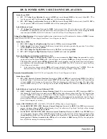
The RED LED
D912
can be used to determine if the B+ to pin
4
of
I901
is present.
Summary of Contents for 46W500
Page 2: ...DP 3X BLANK PAGE NOTES BLANK PAGE ...
Page 6: ...DP 3X BLANK PAGE NOTES BLANK PAGE ...
Page 7: ...DP 3X CHASSIS INFORMATION POWER SUPPLY INFORMATION SECTION 1 ...
Page 8: ...DP 3X BLANK PAGE NOTES BLANK PAGE ...
Page 23: ...DP 3X CHASSIS INFORMATION MICROPROCESSOR INFORMATION SECTION 2 ...
Page 24: ...DP 3X BLANK PAGE NOTES BLANK PAGE ...
Page 35: ...DP 3X CHASSIS INFORMATION VIDEO INFORMATION SECTION 3 ...
Page 36: ...DP 3X BLANK PAGE NOTES BLANK PAGE ...
Page 50: ...DP 3X BLANK PAGE NOTES BLANK PAGE ...
Page 51: ...DP 3X CHASSIS INFORMATION AUDIO INFORMATION SECTION 4 ...
Page 52: ...DP 3X BLANK PAGE NOTES BLANK PAGE ...
Page 57: ...DP 3X CHASSIS INFORMATION DEFLECTION INFORMATION SECTION 5 ...
Page 58: ...DP 3X BLANK PAGE NOTES BLANK PAGE ...
Page 69: ...DP 3X CHASSIS INFORMATION DIGITAL CONVERGENCE INFORMATION SECTION 6 ...
Page 70: ...DP 3X BLANK PAGE NOTES BLANK PAGE ...
Page 83: ...DP 3X CHASSIS INFORMATION ADJUSTMENT INFORMATION SECTION 7 ...
Page 84: ...DP 3X BLANK PAGE NOTES BLANK PAGE ...
Page 98: ...DP 3X BLANK PAGE NOTES BLANK PAGE ...
Page 99: ...DP 3X CHASSIS INFORMATION MISCELLANEOUS INFORMATION SECTION 8 ...
Page 100: ...DP 3X BLANK PAGE NOTES BLANK PAGE ...
Page 111: ...DP 3X CHASSIS INFORMATION DP 33W 46W500 DVD PLAYER TROUBLESHOOTING SECTION 9 ...
Page 112: ...DP 3X BLANK PAGE NOTES BLANK PAGE ...
Page 131: ...DP 3X CHASSIS INFORMATION THINGS YOU SHOULD KNOW SECTION 10 ...
Page 132: ...DP 3X BLANK PAGE NOTES BLANK PAGE ...
Page 134: ...DP 3X BLANK PAGE NOTES BLANK PAGE ...
Page 161: ...DP 3X BLANK PAGE NOTES BLANK PAGE ...
Page 162: ...DP 3X BLANK PAGE NOTES BLANK PAGE ...


