DP-3X SIDE PINCUSHION CIRCUIT EXPLANATION
PAGE 05-09
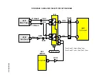
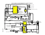
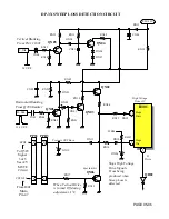
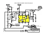
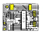
(See the Side Pincushion Circuit Diagram for details)
Due to the nature of deflection, the sides of the picture has a tendencies to pull in similar to an hour glass. The
Side pincushion circuit is responsible for manipulating deflection to compensate. This is accomplished by super
imposing a vertical parabolic waveform on the DC voltage utilized for Horizontal Size.
VERTICAL YOKE CHARGE PULSE:
(See Vertical Output Circuit for details)
The pulse generated on the positive side of
C607
is routed through the parabolic wave form generation circuit of
R621
, and
C608
to the side pincushion circuit.
SIDE PIN WAVE FORM GENERATION IC:
Then through
R742
,
C702
,
R709
to pin
6
of
I701
. This is the
negative
leg of the internal op-amp. Also attached
to this input circuit is the Horizontal Size circuit comprised of
R710
,
R711
,
R713
and clamped by
D714.
The
variable resistor
R711
which adjust the DC level at pin
6
. The
positive
leg of the op-amp is connected through
pin
5
to the feedback circuit from the Side Pin Cushion output circuit for stability.
The output of the DC offset voltage with Vertical parabolic wave form attached is then routed out pin
7
to the
base of
Q703
. This transistor has its emitter off set above ground by
D713
,
R747
back to the
SW +9V
and
R704
.
This transistor drives the base of the Side Pin Cushion modulator transistor
Q701
. The collector of
Q701
is con-
nected to the Deflection SW +115V. The DC offset voltage and Vertical parabolic side pin cushion compensation
wave form is now super imposed on the SW +115V which is sent to the Deflection Transformer
T701
and the
Horizontal Linearity circuit
C715
,
L703
,
R729
and
R756
to the Horizontal Yoke returns.
D SIZE SWITCH:
When Magic Focus is activated by either the Magic Focus button or the customer’s menu or during service when
the sensors are initialized,
Q710
receives the
D Size
command from the Digital Convergence Unit,
UKDG
pin
15 of
PDG
connector. When
Q710
turns on, it bypasses
R714
and lowers the resistance from the emitter of
Q701
to ground. This increases the Horizontal size to allow positive contact of the light pattern hitting the sensors.
Summary of Contents for 46W500
Page 2: ...DP 3X BLANK PAGE NOTES BLANK PAGE ...
Page 6: ...DP 3X BLANK PAGE NOTES BLANK PAGE ...
Page 7: ...DP 3X CHASSIS INFORMATION POWER SUPPLY INFORMATION SECTION 1 ...
Page 8: ...DP 3X BLANK PAGE NOTES BLANK PAGE ...
Page 23: ...DP 3X CHASSIS INFORMATION MICROPROCESSOR INFORMATION SECTION 2 ...
Page 24: ...DP 3X BLANK PAGE NOTES BLANK PAGE ...
Page 35: ...DP 3X CHASSIS INFORMATION VIDEO INFORMATION SECTION 3 ...
Page 36: ...DP 3X BLANK PAGE NOTES BLANK PAGE ...
Page 50: ...DP 3X BLANK PAGE NOTES BLANK PAGE ...
Page 51: ...DP 3X CHASSIS INFORMATION AUDIO INFORMATION SECTION 4 ...
Page 52: ...DP 3X BLANK PAGE NOTES BLANK PAGE ...
Page 57: ...DP 3X CHASSIS INFORMATION DEFLECTION INFORMATION SECTION 5 ...
Page 58: ...DP 3X BLANK PAGE NOTES BLANK PAGE ...
Page 69: ...DP 3X CHASSIS INFORMATION DIGITAL CONVERGENCE INFORMATION SECTION 6 ...
Page 70: ...DP 3X BLANK PAGE NOTES BLANK PAGE ...
Page 83: ...DP 3X CHASSIS INFORMATION ADJUSTMENT INFORMATION SECTION 7 ...
Page 84: ...DP 3X BLANK PAGE NOTES BLANK PAGE ...
Page 98: ...DP 3X BLANK PAGE NOTES BLANK PAGE ...
Page 99: ...DP 3X CHASSIS INFORMATION MISCELLANEOUS INFORMATION SECTION 8 ...
Page 100: ...DP 3X BLANK PAGE NOTES BLANK PAGE ...
Page 111: ...DP 3X CHASSIS INFORMATION DP 33W 46W500 DVD PLAYER TROUBLESHOOTING SECTION 9 ...
Page 112: ...DP 3X BLANK PAGE NOTES BLANK PAGE ...
Page 131: ...DP 3X CHASSIS INFORMATION THINGS YOU SHOULD KNOW SECTION 10 ...
Page 132: ...DP 3X BLANK PAGE NOTES BLANK PAGE ...
Page 134: ...DP 3X BLANK PAGE NOTES BLANK PAGE ...
Page 161: ...DP 3X BLANK PAGE NOTES BLANK PAGE ...
Page 162: ...DP 3X BLANK PAGE NOTES BLANK PAGE ...

