


50VF820/LC58;
No. 0
210
NTSC
LC58/LC58E
R/C: CLU-
3851WL; CLU-4352UG2
TO GO TO A CHAPTER, CLICK ON ITS HEADING BELOW
PA
55VG825/LC58E
60VF820/LC58;
55VF820/LC58;
50VG825/LC58E
60VG825/LC58E
!
TO GO TO A CHAPTER, CLICK ON ITS HEADING BELOW
SERVICE MANUAL
CONTENTS
IMPORTANT SAFETY INSTRUCTIONS .............................................................................. 2
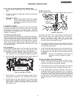
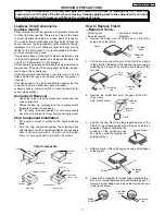
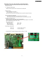
SERVICING PRECAUTIONS ............................................................................................. 4
AGENCY REGULATORY INFORMATION
..
.......................................................................
..
9
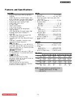
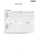
FEATURES & SPECIFICATIONS
.
..................................................................................... 1
0
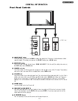
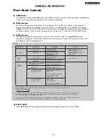
GENERAL INFORMATION ..................................................................................................1
3
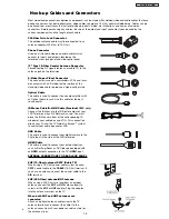
REMOTE CONTROL GUIDE
.............................................
..................................................
2
6
SERVICE ADJUSTMENTS .......
..........................................................................................
31
TROUBLESHOOTING FLOW CHART................................................................................88
BLOCK DIAGRAM .............................................................................................................96
CONNECTION DIAGRAM .................................................................................................98
ASSEMBLY DRAWINGS
.........................................................................................................99
FINAL WIRING DIAGRAM ..................................................................................................................107
QUICK DISASSEMBLY GUIDE ..........................................................................................11
2
WAVEFORMS ..................................................................................................................................1
23
DC VOLTAGE TABLES
...
.................................................................................................1
26
CIRCUIT SCHEMATIC DRAWING
......
................................................................................12
9
PRINTED CIRCUIT BOARDS ...........................................................................................152
REPLACEMENT PARTS LIST
.........................................................................................1
70
QUICK REFERENCE PARTS LIST (IC & UNIT) ..............................................................18
8
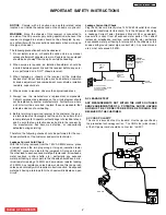
CAUTION:
These servicing instructions are for use by qualified service personnel only. To reduce the risk of
electric shock do not perform any servicing other than that contained in the operating instructions
unless you are qualified to do so. Before servicing this chassis, it is important that the service
technician read the “IMPORTANT SAFETY INSTRUCTIONS” in this service manual.
SAFETY NOTICE
USE ISOLATION TRANSFORMER WHEN SERVICING
Components having special safety characteristics are identified by a on the schematics and on the parts list in this
Service Data and its supplements and bulletins. Before servicing the chassis, it is important that the service technician
read and follow the “Important Safety Instructions” in this Service Manual.
AUGUST
200
5
HHEA-MANUFACTURING DIVISION
LCD REAR PROJECTION TELEVISION
SPECIFICATIONS AND PARTS ARE SUBJECT TO CHANGE FOR IMPROVEMENT
Summary of Contents for 50VF820 - 50" Rear Projection TV
Page 96: ...LC58 LC58E CIRCUIT BLOCK DIAGRAM TABLE OF CONTENTS 96 ...
Page 97: ...LC58 LC58E POWER SUPPLY BLOCK DIAGRAM TABLE OF CONTENTS 97 ...
Page 98: ...CONNECTION DIAGRAM TABLE OF CONTENTS LC58 LC58E 98 ...
Page 105: ...LC58 chassis Model 50VF820 55VF820 60VF820 1 FRONT PANEL 2 REAR PANEL LC58 LC58E 105 ...
Page 106: ...LC58E chassis Model 50VG825 55VG825 60VG825 1 FRONT PANEL 2 REAR PANEL LC58 LC58E 106 ...
Page 155: ...SIGNAL PWB Solder side PRINTED CIRCUIT BOARDS BACK TO TABLE OF CONTENTS LC58 LC58E 155 ...
Page 159: ...PRINTED CIRCUIT BOARDS POWER PWB Solder side BACK TO TABLE OF CONTENTS LC58 LC58E 159 ...
Page 190: ......


