-- 16 -
E. Horizontal Processor
H sync go through TDA4855 internal separation circuit to the first comparator for HOR. Phase ADJ
and then to stage output. A HOR. Drive pulse from pin 7 and input H-sync limit is setting by R431,
R432 and C415.
E-1. Geometric distortion correction
The E-W parabola output from pin 11 is controlled DC CONTROL (pin 20 & 21) and this
parabola go through Q404-Q407 input to pin30 (HOR. Phase ADJ.) for pin-balance ADJ. and
also go through Q408-Q411 for parallel ADJ. And through Q412-Q414 for corner ADJ.
F. Vertical Pre-Amp
VERT. Sync input to VERT. OSC. and generates a saw-tooth at pin 24, the free-run frequency is
setting by R428 and C412 & (fvo=1/10.8 x R428 x C412 & C445), the V-position is controlled by the
D-C (pin 17), and V-size is controlled by D-C (pin 18), and the pin 19 is to ADJ. VERT. linearity.
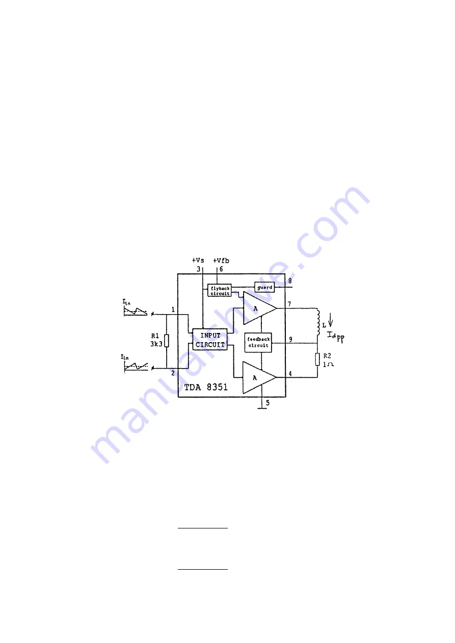
F-1. VERT output circuit U601 (TDA 8351) see
Figure (6)
The saw-tooth is output from U401 pin # 12 & 13. to the pins # 1 and 2 of TDA8351 (vert output
amplifier) and then output from pin # 7 to the vert DY for vert. deflection.
F-2. Horizontal size modulation
To modulation H-size control DC is achieved by applying a parabola to the pins 3 and 5 to
control U402 mono-stable to generate a square wave to drive Q505 thus obtaining a variable
B+ which is input frequency dependent.
31.5KHz T=31.75mS
6.8 to 8.6 mS
HOR.B+=200V x = 43.2 to 54.7V
31.75 mS
95KHZ T=10.526 mS
6.8 to 8.6 mS
HOR.B+=200V x = 130 to165V
10.526 mS
Summary of Contents for CM721FET
Page 10: ... 9 ...
Page 11: ... 10 2 CONTROLS AND CONNECTORS LAYOUT A Main PCB ...
Page 20: ... 19 A Monitor Check Flow Chart A 1 No raster ...
Page 21: ... 20 A 2 No Picture ...
Page 22: ... 21 A 3 No vertical deflection raster become a horizontal line ...
Page 23: ... 22 APPENDIX A SCHEMATIC DIAGRAMS PCB ASSEMBLIES ...
Page 28: ......
Page 29: ......
Page 30: ......
Page 31: ...THE UPDATED PARTS LIST FOR THIS MODEL IS AVAILABLE ON ESTA ...
Page 32: ... 50 APPENDIX C DISPLAY UNIT ASSEMBLY ...
Page 33: ......
Page 36: ......


