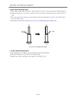

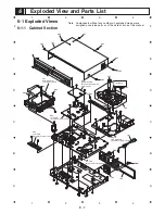


4
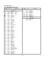
3
2
1
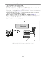
A
B
C
D
E
F
A
B
C
D
E
F
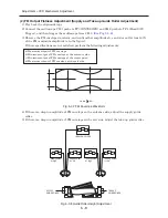
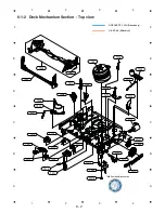
8
7
6
5
4
3
2
1
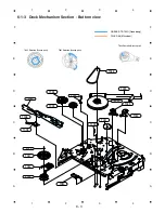
8
7
6
5
S - 1
S
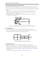
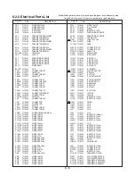
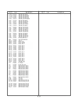
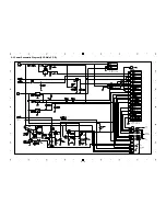
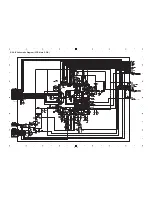
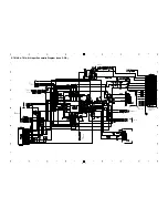
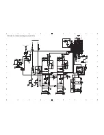
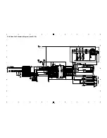
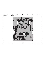
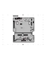
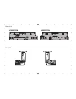
SCHEMATIC,WIRING DIAGRAMS
S-1 Wiring Diagram
For schematic Diagram
- Resistors are in ohms, 1/8W unless otherwise noted.
Special note :
Most semiconductor devices are electrostatically sensitive and therefore require the
special handling techniques described under the "Electrostatic Protection
Measures" section of this service manual.
Note :
Do not use the part number shown on this drawing for ordering. The correct part
number is shown in the parts list (may be slightly different or amended since this
drawing was prepared).
Important safety notices :
Components identified with the mark have the special characteristics for safety.
When replacing any of these components.
Use only the same type.
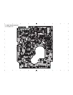
1
2
3
4
5
6
7
8
9
10
11
12
13
14
15
16
17
18
19
20
21
22
23
24
25
26
27
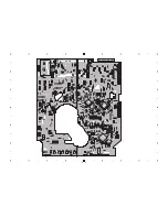
33
32
31
30
29
28
27
26
25
24
23
22
21
20
19
18
17
16
15
14
13
12
11
10
9
8
7
6
5
4
3
2
1
33
32
31
30
29
28
27
26
25
24
23
22
21
20
19
18
17
16
15
14
13
12
11
10
9
8
7
6
5
4
3
2
1
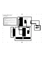
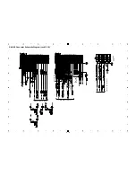
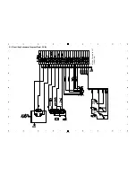
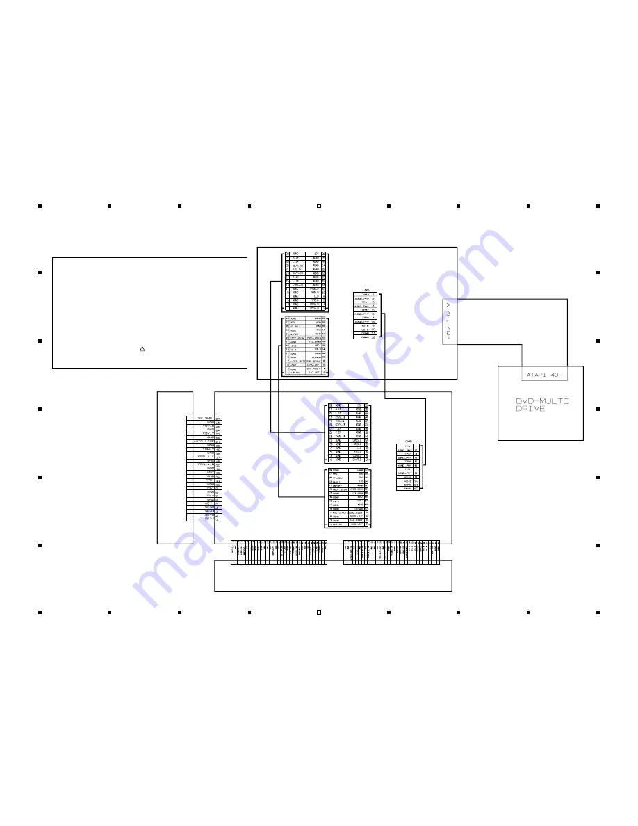
FRONT
P
.C.B
JACK P.C.B
DVD MAIN P.C.B
VCR MAIN P.C.B
FJACK1
CN4
CN3
MCON1
CN02
CN01
MCON2
FJACK2
ATCN1B