Chapter 2 Specifications
2 – 8
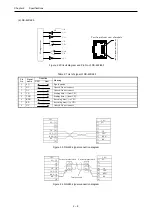
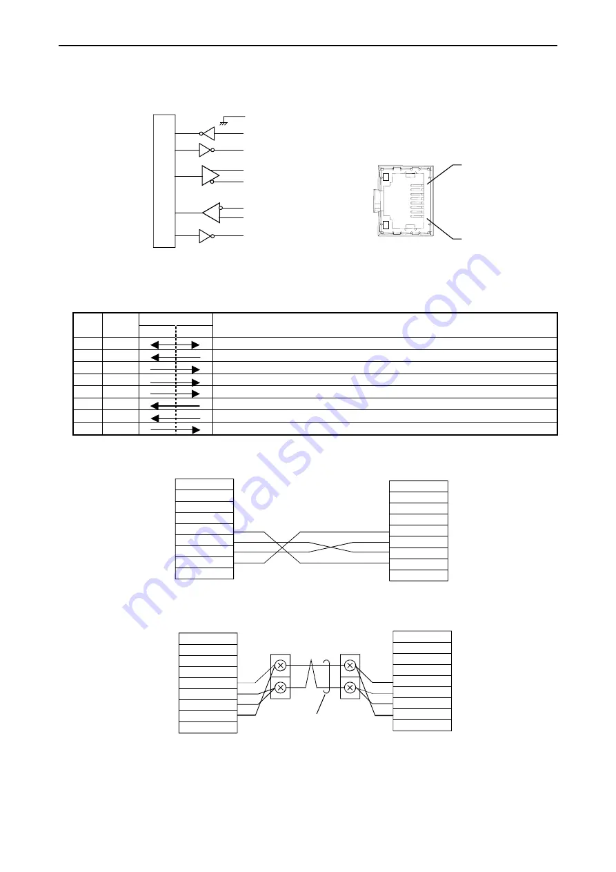
(2) RS-422/485
[1]SG
[4]TX
[5]TXN
[6]RXN
[7]RX
[8]N.C.
M
icr
op
ro
ce
sso
r
[2]N.C.
[3]N.C.
[1]
[2]
[3]
[4]
[5]
[6]
[7]
[8]
Port from a front view of module
Figure 2.2 Circuit diagram and Pin No. of RS-422/485
Table 2.7 List of signal of RS-422/485
Direction
Pin
No.
Signal
name
CPU Host
Meaning
1 SG
Signal
ground
2
N.C.
Unused. Do not connect.
3
N.C.
Unused. Do not connect.
4
TX
Sending data (+) from CPU
5
TXN
Sending data (–) from CPU
6
RXN
Receiving data (–) to CPU
7
RX
Receiving data (+) to CPU
8
N.C.
Unused. Do not connect.
CPU
SG
TX
TXN
RXN
RX
[1]
[2]
[3]
[4]
[5]
[6]
[7]
[8]
CPU
[1]
[2]
[3]
[4]
[5]
[6]
[7]
[8]
SG
TX
TXN
RXN
RX
Figure 2.3 RS-422 signal connection diagram
A
B
External terminal block
Twist pair cable
CPU
SG
TX
TXN
RXN
RX
[1]
[2]
[3]
[4]
[5]
[6]
[7]
[8]
CPU
[1]
[2]
[3]
[4]
[5]
[6]
[7]
[8]
SG
TX
TXN
RXN
RX
External terminal block
Figure 2.4 RS-485 signal connection diagram

