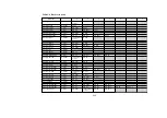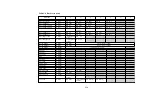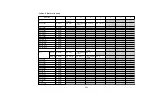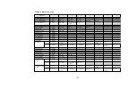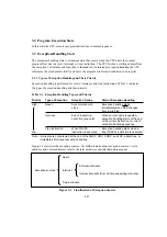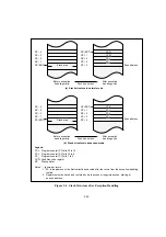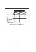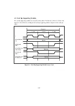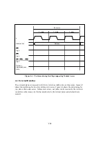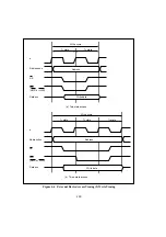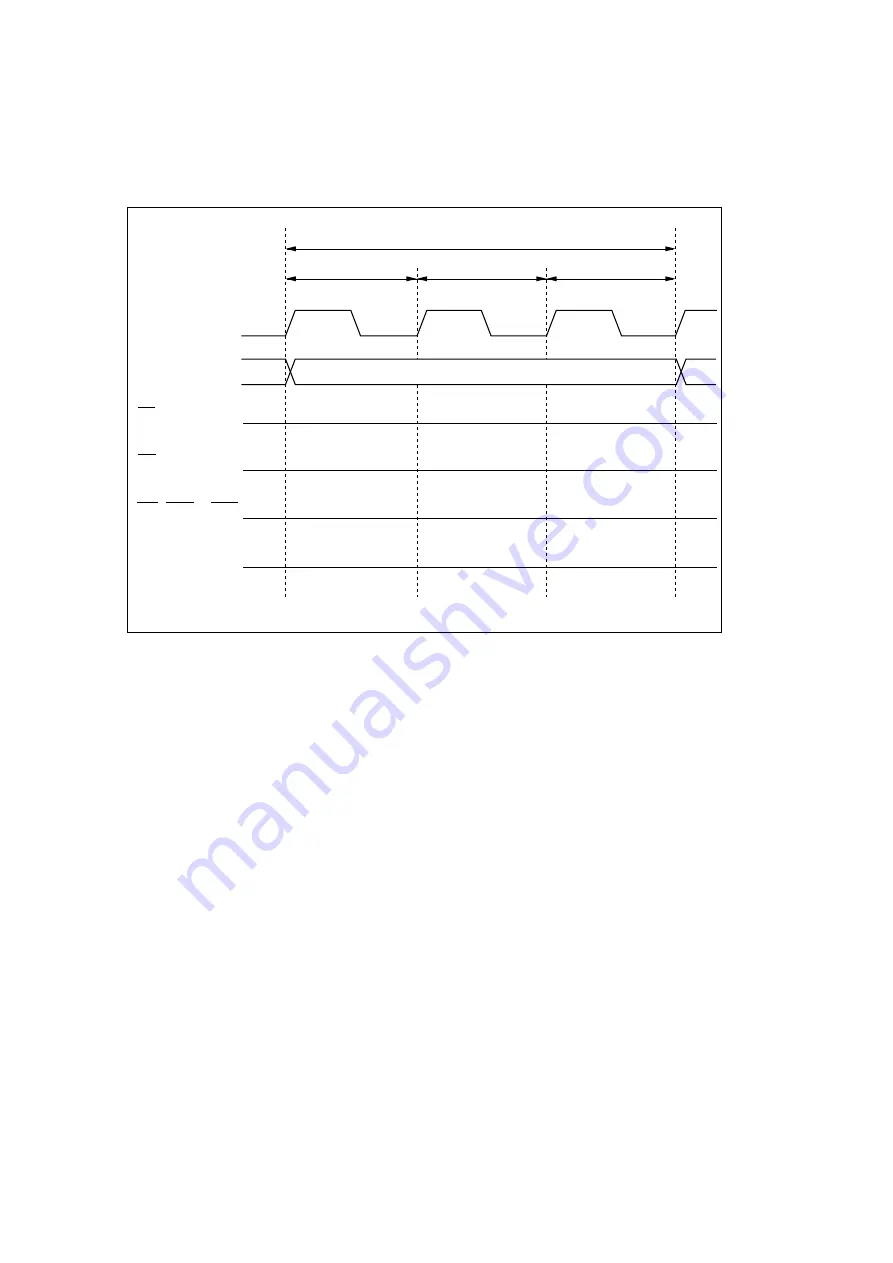
Figure 4-4 Pin States during On-Chip Supporting Module Access
4.4 External Data Bus
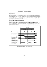
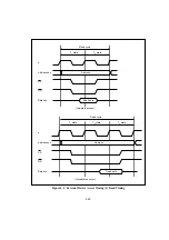
The external data bus is accessed with 8-bit or 16-bit bus width in two or three states. Figure 4-5
shows the read timing for two-state or three-state access. Figure 4-6 shows the write timing for
two-state or three-state access. In three-state access, wait states can be inserted by the wait-state
controller or other means. For further details refer to the relevant microcontroller hardware
manual.
Bus cycle
T
1
state
T
2
state
Address
Address bus
AS
High
RD
High
WR (HWR or LWR)
High
Data bus
high-impedance
state
ø
T
3
state
248

