


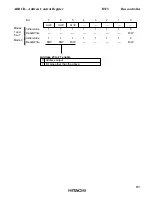


637
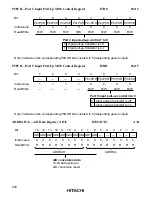
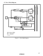
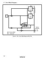
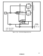
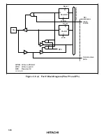
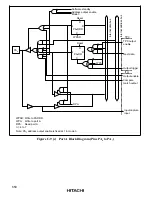
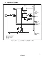
C.3 Port 3 Block Diagram
Internal data bus (upper)
Internal data bus (lower)
P3
n
DDR
Reset
Modes 6 and 7
R
Q
D
C
Reset
R
Q
D
P3
n
DR
WP3D
WP3
C
RP3
Modes
1, 3, and 5
Modes 6 and 7
P3
n
WP3D:
WP3:
RP3:
n = 0 to 7
Write to P3DDR
Write to port 3
Read port 3
Write to external
address
Hardware
standby
Read external
address
Figure C-3 Port 3 Block Diagram


