150
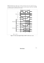
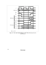
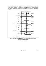
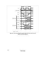
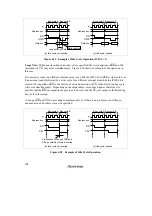
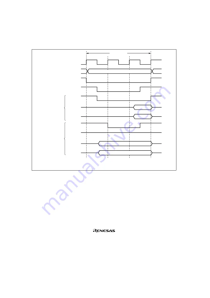
16-Bit, Three-State-Access Areas: Figures 6.11 to 6.13 show the timing of bus control signals
for a 16-bit, three-state-access area. In these areas, the upper data bus (D
15
to D
8
) is used in
accesses to even addresses and the lower data bus (D
7
to D
0
) in accesses to odd addresses. Wait
states can be inserted.
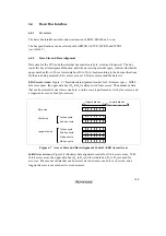
Bus cycle
Even external address in area n
Valid
Invalid
Valid
High
φ
Address bus
CS
n
AS
RD
D
15
to D
8
D
7
to D
0
HWR
LWR
D
15
to D
8
D
7
to D
0
Read access
Write access
Note: n = 7 to 0
T
1
T
2
T
3
Undetermined data
Figure 6.11 Bus Control Signal Timing for 16-Bit, Three-State-Access Area (1)
(Byte Access to Even Address)
Summary of Contents for H8/3060
Page 10: ......
Page 16: ......
Page 114: ...66 ...
Page 132: ...84 ...
Page 144: ...96 ...
Page 170: ...122 ...
Page 212: ...164 ...
Page 268: ...220 ...
Page 332: ...284 ...
Page 396: ...348 ...
Page 494: ...446 ...
Page 698: ...650 ...
Page 748: ...700 H8 3064F ZTAT B mask version Ports 1 2 5 LED 600 Ω Figure 22 8 Sample LED Circuit ...
Page 777: ...729 H8 3062F ZTAT B mask version Ports 1 2 5 LED 600 Ω Figure 22 14 Sample LED Circuit ...
Page 810: ...762 ...
Page 994: ...946 ...


