218
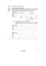
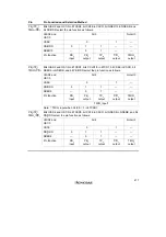
Table 7.24
Port B Pin Functions (Modes 6 and 7)
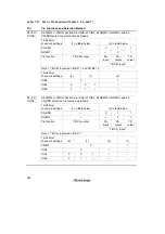
Pin
Pin Functions and Selection Method
PB
7
/TP
15
Bit NDER15 in NDERB and bit PB
7
DDR select the pin function as follows.
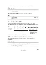
PB
7
DDR
0
1
1
NDER15
—
0
1
Pin function
PB
7
input
PB
7
output
TP
15
output
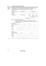
PB
6
/TP
14
Bit NDER14 in NDERB and bit PB
6
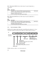
DDR select the pin function as follows.
PB
6
DDR
0
1
1
NDER14
—
0
1
Pin function
PB
6
input
PB
6
output
TP
14
output
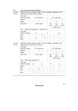
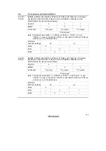
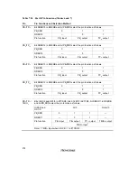
PB
5
/TP
13
Bit NDER13 in NDERB and bit PB
5
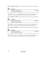
DDR select the pin function as follows.
PB
5
DDR
0
1
1
NDER13
—
0
1
Pin function
PB
5
input
PB
5
output
TP
13
output
PB
4
/TP
12
Bit NDER12 in NDERB and bit PB
4
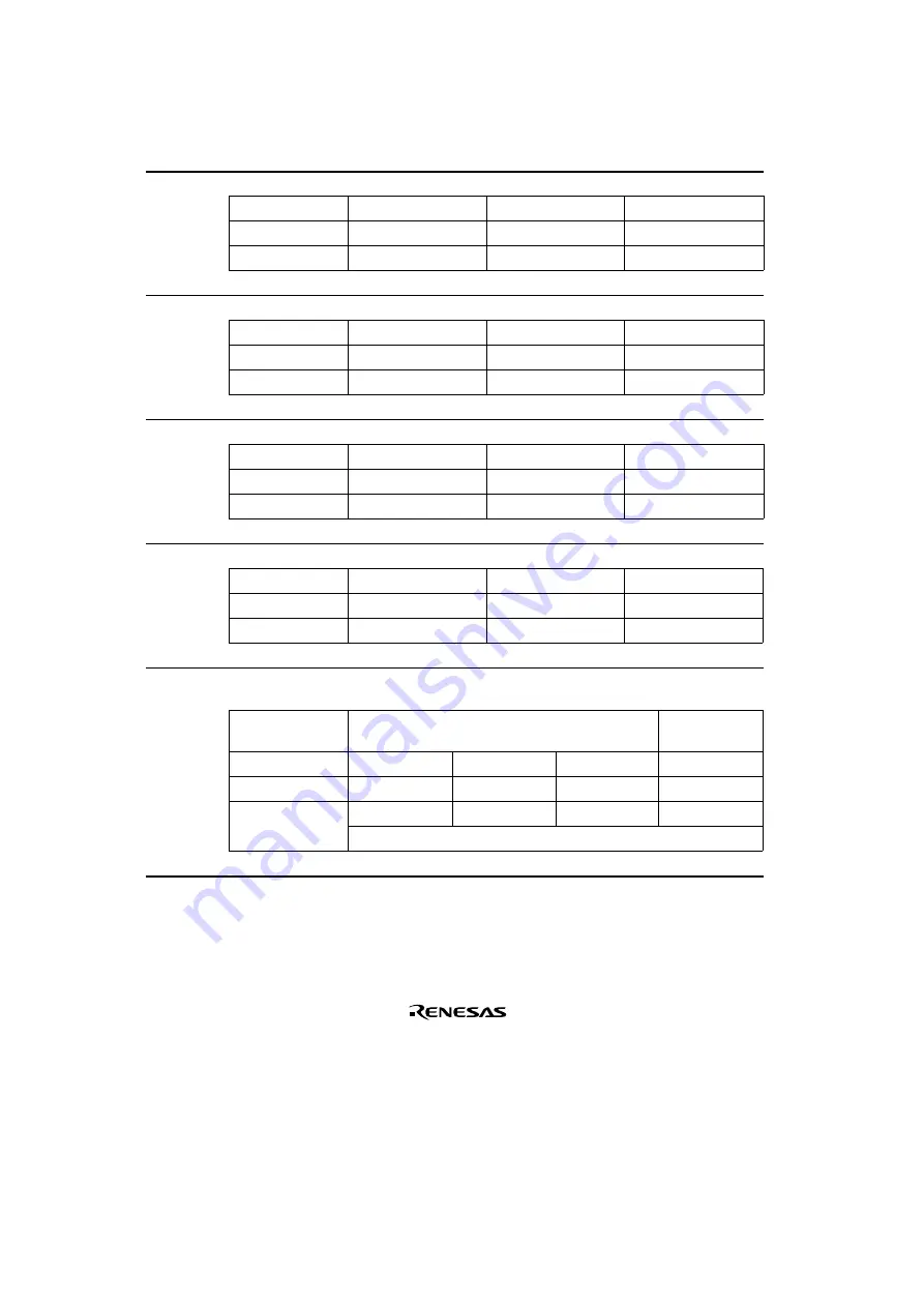
DDR select the pin function as follows.
PB
4
DDR
0
1
1
NDER12
—
0
1
Pin function
PB
4
input
PB
4
output
TP
12
output
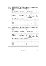
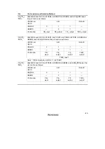
PB
3
/TP
11
/
TMIO
3
Bits OIS3/2 and OS1/0 in 8TCSR3, bits CCLR1/0 in 8TCR3, bit NDER11 in NDERB,
and bit PB
3
DDR select the pin function as follows.
OIS3/2 and
OS1/0
All 0
Not all 0
PB
3
DDR
0
1
1
—
NDER11
—
0
1
—
Pin function
PB
3
input
PB
3
output
TP
11
output
TMIO
3
output
TMIO
3
input
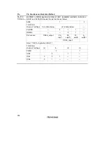
*
Note:
*
TMIO
3
input when bit ICE = 1 in 8TCSR3.
Summary of Contents for H8/3060
Page 10: ......
Page 16: ......
Page 114: ...66 ...
Page 132: ...84 ...
Page 144: ...96 ...
Page 170: ...122 ...
Page 212: ...164 ...
Page 268: ...220 ...
Page 332: ...284 ...
Page 396: ...348 ...
Page 494: ...446 ...
Page 698: ...650 ...
Page 748: ...700 H8 3064F ZTAT B mask version Ports 1 2 5 LED 600 Ω Figure 22 8 Sample LED Circuit ...
Page 777: ...729 H8 3062F ZTAT B mask version Ports 1 2 5 LED 600 Ω Figure 22 14 Sample LED Circuit ...
Page 810: ...762 ...
Page 994: ...946 ...

