329
10.2.5
Next Data Register A (NDRA)
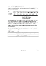
NDRA is an 8-bit readable/writable register that stores the next output data for TPC output groups
1 and 0 (pins TP
7
to TP
0
). During TPC output, when an 16-bit timer compare match event
specified in TPCR occurs, NDRA contents are transferred to the corresponding bits in PADR. The
address of NDRA differs depending on whether TPC output groups 0 and 1 have the same output
trigger or different output triggers.
NDRA is initialized to H'00 by a reset and in hardware standby mode. It is not initialized in
software standby mode.
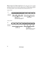
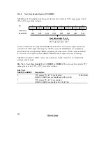
Same Trigger for TPC Output Groups 0 and 1: If TPC output groups 0 and 1 are triggered by
the same compare match event, the NDRA address is H'FFFA5. The upper 4 bits belong to group
1 and the lower 4 bits to group 0. Address H'FFFA7 consists entirely of reserved bits that cannot
be modified and always read 1.
Address H'FFFA5
Bit
Initial value
Read/Write
0
NDR0
0
R/W
1
NDR1
0
R/W
2
NDR2
0
R/W
3
NDR3
0
R/W
4
NDR4
0
R/W
5
NDR5
0
R/W
6
NDR6
0
R/W
7
NDR7
0
R/W
Next data 7 to 4
These bits store the next output
data for TPC output group 1
Next data 3 to 0
These bits store the next output
data for TPC output group 0
Address H'FFFA7
Bit
Initial value
Read/Write
0
—
1
—
1
—
1
—
2
—
1
—
3
—
1
—
4
—
1
—
5
—
1
—
6
—
1
—
7
—
1
—
Reserved bits
Summary of Contents for H8/3060
Page 10: ......
Page 16: ......
Page 114: ...66 ...
Page 132: ...84 ...
Page 144: ...96 ...
Page 170: ...122 ...
Page 212: ...164 ...
Page 268: ...220 ...
Page 332: ...284 ...
Page 396: ...348 ...
Page 494: ...446 ...
Page 698: ...650 ...
Page 748: ...700 H8 3064F ZTAT B mask version Ports 1 2 5 LED 600 Ω Figure 22 8 Sample LED Circuit ...
Page 777: ...729 H8 3062F ZTAT B mask version Ports 1 2 5 LED 600 Ω Figure 22 14 Sample LED Circuit ...
Page 810: ...762 ...
Page 994: ...946 ...

