623
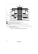
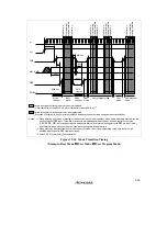
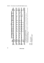
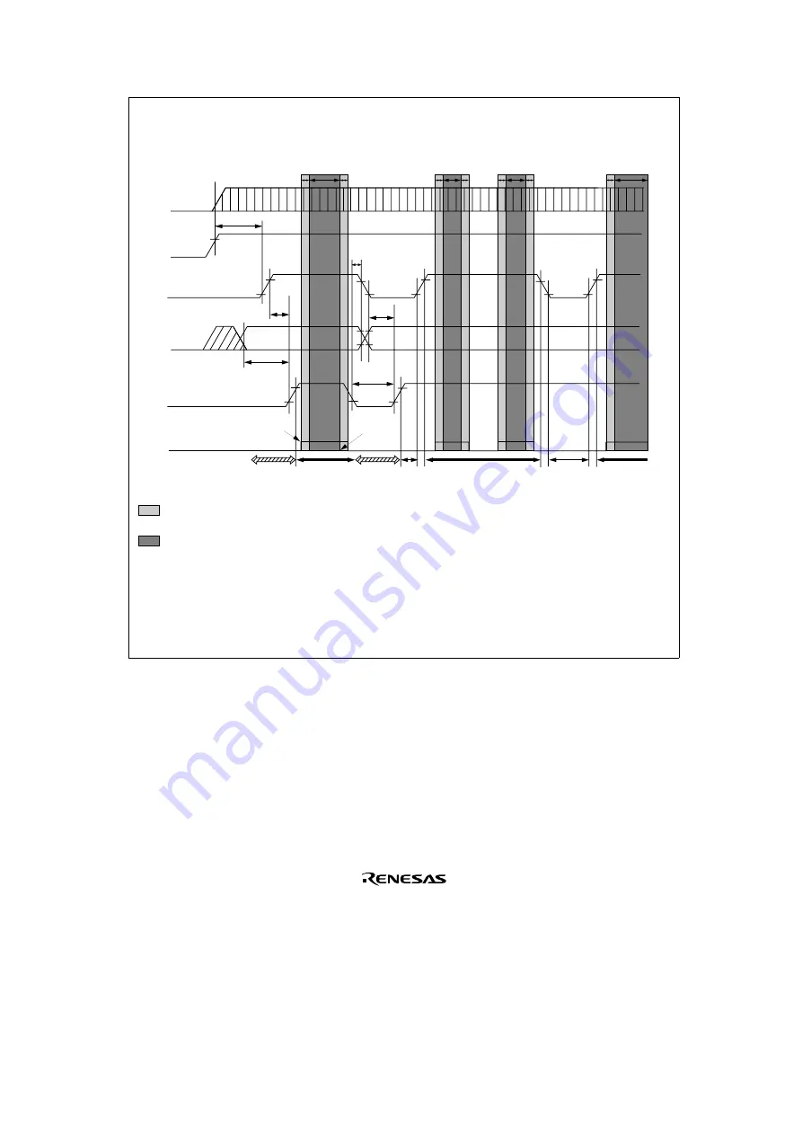
Period during which flash memory access is prohibited
(x: Wait time after setting SWE bit, y: Wait time after clearing SWE bit)
*
3
Period during which flash memory can be programmed
(Execution of program in flash memory prohibited, and data reads other than verify operations prohibited)
φ
V
CC
FWE
t
OSC1
Min 0
µ
s
t
MDS
t
MDS
t
MDS
t
RESW
MD
2
to MD
0
RES
SWE bit
Mode
change
*
1
User
mode
Boot
mode
User program mode
SWE set
SWE
cleared
*
2
Programming/
erasing possible
Wait time: x
Wait time: y
Programming/
erasing possible
Wait time: x
Wait time: y
Programming/
erasing possible
Wait time: x
Programming/
erasing possible
Wait time: x
Wait time: y
Mode
change
*
1
User
mode
User program
mode
Notes:
*
1 When entering boot mode or making a transition from boot mode to another mode, mode switching must be carried
out by means of
RES
input. The state of ports with multiplexed address functions and bus control output pins
(
CSn
,
AS
,
RD
,
WR
) will change during this switchover interval (the interval during which the
RES
pin input is low),
and therefore these pins should not be used as output signals during this time.
*
2 When making a transition from boot mode to another mode, the mode programming setup time t
MDS
must be
satisfied with respect to
RES
clearance timing.
*
3 See 22.5.6 Flash Memory Characteristics.
Figure 19.18 Mode Transition Timing
(Example: Boot Mode
→
→
→
→
User Mode
↔
↔
↔
↔
User Program Mode)
Summary of Contents for H8/3060
Page 10: ......
Page 16: ......
Page 114: ...66 ...
Page 132: ...84 ...
Page 144: ...96 ...
Page 170: ...122 ...
Page 212: ...164 ...
Page 268: ...220 ...
Page 332: ...284 ...
Page 396: ...348 ...
Page 494: ...446 ...
Page 698: ...650 ...
Page 748: ...700 H8 3064F ZTAT B mask version Ports 1 2 5 LED 600 Ω Figure 22 8 Sample LED Circuit ...
Page 777: ...729 H8 3062F ZTAT B mask version Ports 1 2 5 LED 600 Ω Figure 22 14 Sample LED Circuit ...
Page 810: ...762 ...
Page 994: ...946 ...

