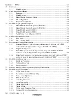
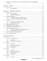
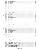
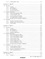
background image

Hitachi Single-Chip Microcomputer

H8S/2199 Series

H8S/2199

HD6432199

H8S/2198

HD6432198

H8S/2197

HD6432197

H8S/2196

HD6432196

H8S/2199F-ZTAT

HD64F2199

Hardware Manual

ADE-602-191

Rev 1.0
2/15/00
Hitachi, Ltd.

Summary of Contents for H8S/2196

Page 1: ...tachi Single Chip Microcomputer H8S 2199 Series H8S 2199 HD6432199 H8S 2198 HD6432198 H8S 2197 HD6432197 H8S 2196 HD6432196 H8S 2199F ZTAT HD64F2199 Hardware Manual ADE 602 191 Rev 1 0 2 15 00 Hitachi Ltd ...

Page 2: ...of bodily injury such as aerospace aeronautics nuclear power combustion control transportation traffic safety equipment or medical equipment for life support 4 Design your application so that the product is used within the ranges guaranteed by Hitachi particularly for maximum rating operating supply voltage range heat radiation characteristics installation conditions and other characteristics Hita...

Page 3: ...sters 27 2 4 3 Control Registers 28 2 4 4 Initial Register Values 29 2 5 Data Formats 30 2 5 1 General Register Data Formats 30 2 5 2 Memory Data Formats 32 2 6 Instruction Set 33 2 6 1 Overview 33 2 6 2 Instructions and Addressing Modes 34 2 6 3 Table of Instructions Classified by Function 35 2 6 4 Basic Instruction Formats 45 2 6 5 Notes on Use of Bit Manipulation Instructions 46 2 7 Addressing ...

Page 4: ... 1 Standby Control Register SBYCR 72 4 2 2 Low Power Control Register LPWRCR 74 4 2 3 Timer Register A TMA 76 4 2 4 Module Stop Control Register MSTPCR 77 4 3 Medium Speed Mode 78 4 4 Sleep Mode 79 4 4 1 Sleep Mode 79 4 4 2 Clearing Sleep Mode 79 4 5 Module Stop Mode 80 4 5 1 Module Stop Mode 80 4 6 Standby Mode 81 4 6 1 Standby Mode 81 4 6 2 Clearing Standby Mode 81 4 6 3 Setting Oscillation Sett...

Page 5: ... 1 System Control Register SYSCR 100 6 2 2 Interrupt Control Registers A to D ICRA to ICRD 101 6 2 3 IRQ Enable Register IENR 102 6 2 4 IRQ Edge Select Registers IEGR 103 6 2 5 IRQ Status Register IRQR 104 6 2 6 Port Mode Register PMR1 105 6 3 Interrupt Sources 106 6 3 1 External Interrupts 106 6 3 2 Internal Interrupts 107 6 3 3 Interrupt Exception Vector Table 108 6 4 Interrupt Operation 111 6 4...

Page 6: ...to H 3FFFF and n 2 when the target address range is H 40000 to H 47FFF 147 7 5 2 Program Verify Mode 148 7 5 3 Erase Mode n 1 when the target address range is H 00000 to H 3FFFF and n 2 when the target address range is H 40000 to H 47FFF 150 7 5 4 Erase Verify Mode n 1 when the target address range is H 00000 to H 3FFFF and n 2 when the target address range is H 40000 to H 47FFF 152 7 6 Flash Memo...

Page 7: ...uty Adjustment Circuit 181 9 5 Medium Speed Clock Divider 181 9 6 Bus Master Clock Selection Circuit 181 9 7 Subclock Oscillator Circuit 182 9 7 1 Connecting 32 768 kHz Crystal Resonator 182 9 7 2 When Subclock is not Needed 183 9 8 Subclock Waveform Shaping Circuit 183 9 9 Notes on the Resonator 183 Section 10 I O Port 185 10 1 Overview 185 10 1 1 Port Functions 185 10 1 2 Port Input 185 10 1 3 M...

Page 8: ...ation 226 10 7 5 Pin States 227 10 8 Port 7 228 10 8 1 Overview 228 10 8 2 Register Configuration 229 10 8 3 Pin Functions 234 10 8 4 Operation 235 10 8 5 Pin States 236 10 9 Port 8 237 10 9 1 Overview 237 10 9 2 Register Configuration 238 10 9 3 Pin Functions 244 10 9 4 Pin States 246 Section 11 Timer A 247 11 1 Overview 247 11 1 1 Features 247 11 1 2 Block Diagram 248 11 1 3 Register Configurati...

Page 9: ... 12 3 3 Event Counter 260 Section 13 Timer J 261 13 1 Overview 261 13 1 1 Features 261 13 1 2 Block Diagram 261 13 1 3 Pin Configuration 263 13 1 4 Register Configuration 263 13 2 Register Descriptions 264 13 2 1 Timer Mode Register J TMJ 264 13 2 2 Timer J Control Register TMJC 267 13 2 3 Timer J Status Register TMJS 270 13 2 4 Timer Counter J TCJ 271 13 2 5 Timer Counter K TCK 271 13 2 6 Timer L...

Page 10: ...ter 1 TMRCP1 299 15 2 5 Timer R Capture Register 2 TMRCP2 300 15 2 6 Timer R Load Register 1 TMRL1 300 15 2 7 Timer R Load Register 2 TMRL2 301 15 2 8 Timer R Load Register 3 TMRL3 301 15 2 9 Module Stop Control Register MSTPCR 302 15 3 Operation 303 15 3 1 Reload Timer Counter Equipped with Capturing Function TMRU 1 303 15 3 2 Reload Timer Counter Equipped with Capturing Function TMRU 2 304 15 3 ...

Page 11: ...ing 336 16 3 6 Input Capture Flag ICFA through ICFD Setting Up Timing 337 16 3 7 Output Comparing Flag OCFA and OCFB Setting Up Timing 338 16 3 8 Overflow Flag CVF Setting Up Timing 338 16 4 Operation Mode of Timer X1 339 16 5 Interrupt Causes 340 16 6 Exemplary Uses of Timer X1 341 16 7 Precautions when Using Timer X1 342 16 7 1 Competition between Writing and Clearing with the FRC 342 16 7 2 Com...

Page 12: ...R0 PWR1 PWR2 PWR3 363 18 2 2 8 bit PWM Control Register PW8CR 364 18 2 3 Port Mode Register 3 PMR3 365 18 2 4 Module Stop Control Register MSTPCR 366 18 3 8 Bit PWM Operation 367 Section 19 12 Bit PWM 369 19 1 Overview 369 19 1 1 Features 369 19 1 2 Block Diagram 370 19 1 3 Pin Configuration 371 19 1 4 Register Configuration 371 19 2 Register Descriptions 372 19 2 1 12 Bit PWM Control Registers CP...

Page 13: ...ing Pin 396 21 4 6 Frequency Division Clock Output 396 Section 22 Serial Communication Interface 1 SCI1 397 22 1 Overview 397 22 1 1 Features 397 22 1 2 Block Diagram 399 22 1 3 Pin Configuration 400 22 1 4 Register Configuration 400 22 2 Register Descriptions 401 22 2 1 Receive Shift Register 1 RSR1 401 22 2 2 Receive Data Register 1 RDR1 401 22 2 3 Transmit Shift Register 1 TSR1 402 22 2 4 Trans...

Page 14: ...DC Switch Register DDCSWR 485 23 2 9 Module Stop Control Register MSTPCR 488 23 3 Operation 489 23 3 1 I 2 C Bus Data Format 489 23 3 2 Master Transmit Operation 490 23 3 3 Master Receive Operation 494 23 3 4 Slave Receive Operation 496 23 3 5 Slave Transmit Operation 499 23 3 6 IRIC Setting Timing and SCL Control 500 23 3 7 Automatic Switching from Formatless Transfer to I 2 C Bus Format Transfer...

Page 15: ...on 532 25 2 Register Descriptions 532 25 2 1 Address Trap Control Register ATCR 532 25 2 2 Trap Address Register 2 to 0 TAR2 to TAR0 534 25 3 Precautions in Usage 535 25 3 1 Basic Operations 535 25 3 2 Enabling 537 25 3 3 Bcc Instruction 537 25 3 4 BSR Instruction 541 25 3 5 JSR Instruction 542 25 3 6 JMP Instruction 544 25 3 7 RTS Instruction 545 25 3 8 SLEEP Instruction 546 25 3 9 Competing Inte...

Page 16: ... 4 Register Description 615 26 6 Drum Speed Error Detector 618 26 6 1 Overview 618 26 6 2 Block Diagram 618 26 6 3 Register Configuration 620 26 6 4 Register Description 621 26 6 5 Operation 626 26 6 6 fH Correction in Trick Play Mode 628 26 7 Drum Phase Error Detector 629 26 7 1 Overview 629 26 7 2 Block Diagram 630 26 7 3 Register Configuration 631 26 7 4 Register Description 632 26 7 5 Operatio...

Page 17: ...er Configuration 679 26 12 4 Register Description 679 26 12 5 Additional V Pulse Signal 681 26 13 CTL Circuit 684 26 13 1 Overview 684 26 13 2 Block Diagram 685 26 13 3 Pin Configuration 686 26 13 4 Register Configuration 686 26 13 5 Register Description 687 26 13 6 Operation 701 26 13 7 CTL Input Section 704 26 13 8 Duty Discriminator 707 26 13 9 CTL Output Section 713 26 13 10 Trapezoid Waveform...

Page 18: ...eshold Register VVTHR 773 27 2 6 Field Detection Window Register FWIDR 775 27 2 7 H Complement and Mask Timing Register HCMMR 777 27 2 8 Noise Detection Counter NDETC 779 27 2 9 Noise Detection Level Register NDETR 780 27 2 10 Data Slicer Detection Window Register DDETWR 781 27 2 11 Internal Sync Frequency Register INFRQR 783 27 3 Operation 784 27 3 1 Selecting Source Signals for Sync Separation 7...

Page 19: ...4 29 2 2 Character Configuration 825 29 2 3 On Screen Display Configuration 826 29 3 Settings in Character Units 827 29 3 1 Character Configuration 827 29 3 2 Character Colors 827 29 3 3 Halftones Cursors 828 29 3 4 Blinking 829 29 3 5 Button Display 830 29 3 6 Character Data ROM OSDROM 831 29 3 7 Display Data RAM OSDRAM 833 29 4 Settings in Row Units 838 29 4 1 Button Patterns 838 29 4 2 Display ...

Page 20: ...or AFC and Dot Clock 872 29 9 1 Sync Signals 872 29 9 2 AFC Circuit 872 29 9 3 Dot Clock 872 29 9 4 4 2fsc 873 29 10 OSD Operation in CPU Operation Modes 875 29 11 Character Data ROM OSDROM Access by CPU 876 29 11 1 Serial Timer Control Register STCR 876 Section 30 Electrical Characteristics 877 30 1 Absolute Maximum Ratings 877 30 2 Electrical Characteristics of HD6432199 HD6432198 HD6432197 and ...

Page 21: ...racteristics of HD64F2199 918 Appendix A Instruction Set 923 A 1 Instructions 923 A 2 Instruction Codes 934 A 3 Operation Code Map 944 A 4 Number of Execution States 948 A 5 Bus Status during Instruction Execution 958 A 6 Change of Condition Codes 972 Appendix B Internal I O Registers 977 B 1 Addresses 977 B 2 Function List 986 Appendix C Pin Circuit Diagrams 1116 C 1 Pin Circuit Diagrams 1116 App...

Page 22: ... the object code level facilitating migration from the H8 300 H8 300L or H8 300H Series The H8S 2199 Series is equipped with a digital servo circuit sync separator OSD data slicer ROM RAM seven types of timers three types of PWM two types of serial communication interface an I 2 C bus interface A D converter and I O port as on chip supporting modules The on chip ROM is either flash memory F ZTAT o...

Page 23: ...16 32 bit transfer arithmetic and logic instructions Unsigned signed multiply and divide instructions Powerful bit manipulation instructions CPU operating modes Advanced mode 16 Mbyte address space Timer Seven types of timer are incorporated Timer A 8 bit interval timer Clock source can be selected among 8 types of internal clock of which frequencies are divided from the system clock φ and subcloc...

Page 24: ... internal clock and DVCFG Two output compare outputs Four input capture inputs Watchdog timer Functions as watchdog timer or 8 bit interval timer Generates reset signal or NMI at overflow Prescaler unit Divides system clock frequency and generates frequency division clock for supporting module functions Divides subclock frequency and generates input clock for Timer A clock time base Generates 8 bi...

Page 25: ...onversion time 10 MHz operation Sample and hold function A D conversion can be activated by software or external trigger Address trap controller Interrupt occurs when the preset address is found during bus cycle To be trapped addresses can be individually set at three different locations I O port 56 input output pins 8 input only pins Can be switched for each supporting module Servo circuit Digita...

Page 26: ...Sampling clock generated by AFC Slice interrupt Error detection Flash memory or mask ROM Refer to the product line up High speed static RAM Product Name ROM RAM H8S 2199 128 k bytes 3 k bytes H8S 2198 112 k bytes 3 k bytes H8S 2197 96 k bytes 3 k bytes H8S 2196 80 k bytes 3 k bytes Memory Power down state Medium speed mode Sleep mode Module stop mode Standby mode Subclock operation Subactive mode ...

Page 27: ...erator 8 to 10 MHz Subclock pulse generator 32 768 kHz Packages 112 pin plastic QFP FP 112 Product lineup Note F ZTAT version Product Code Series Mask ROM Versions F ZTAT Versions ROM RAM bytes Packages HD6432199 HD64F2199 128 k 3 k 256 k 8 k FP 112 HD6432198 112 k 3 k FP 112 HD6432197 96 k 3 k FP 112 H8S 2199 HD6432196 80 k 3 k FP 112 ...

Page 28: ...ontroller Address trap controller P16 P11 P17 TMOW P10 P14 P03 AN3 P05 AN5 P02 AN2 P06 AN6 P01 AN1 P07 AN7 P00 AN0 P04 AN4 ANA AN9 AN8 ANB AVCC AVSS P83 C Rotary R P85 COMP B P82 EXCTL P86 EXTTRG P81 EXCAP YBO P87 DPG P80 YCO P84 H Amp SW G P33 PWM1 P35 PWM3 P32 PWM0 P36 BUZZ P31 SV2 P37 TMO P30 SV1 P34 PWM2 P43 FTIC P45 FTOA P42 FTIB P46 FTOB P41 FTIA P47 RPTRG P40 PWM14 P44 FTID P73 PPG3 P75 PPG...

Page 29: ...sync VCC VCC P35 PWM3 P36 BUZZ P37 TMO P60 RP0 P61 RP1 P62 RP2 P63 RP3 P64 RP4 P65 RP5 P66 RP6 P67 RP7 TMBI P17 TMOW P16 P15 P14 P13 P12 P11 P10 AVCC P00 AN0 P01 AN1 P02 AN2 P03 AN3 P04 AN4 P05 AN5 P06 AN6 1 SV SS FP 112 Top view 84 2 CTLREF 83 3 CTL 82 4 CTL 81 5 CTLBias 80 6 CTLFB 79 7 CTLAmp o 78 8 CTLSMT i 77 9 CFG 76 10 SV CC 75 11 AFCpc 74 12 AFCosc 73 13 AFCLPF 72 14 Csync Hsync 71 15 VLPF ...

Page 30: ...ed to the system power supply 5V when the A D converter is not used AVSS 23 Input Analog ground Ground pin for A D converter It should be connected to the system power supply 0V OVCC 18 Input OSD power supply VCC OSD should be connected to the OSD analog power supply 5 V OVSS 20 Input OSD ground VSS OSD should be connected to the OSD analog power supply 0 V Power supply VCL 81 Input Smoothing capa...

Page 31: ... 545 546 547 548 38 39 40 41 42 Input External interrupt requests 1 to 5 External interrupt input pins for which rising or falling edge sense are selectable 43 Input Input capture input Input capture input pin for prescaler unit Prescaler unit TMOW 44 Output Frequency division clock output Output pin for clock of which frequency is divided by prescaler TMBI 45 Input Timer B event input Input pin f...

Page 32: ...ated by 8 bit PWM 0 1 2 and 3 PWM PWM14 73 Output 14 bit PWM square waveform output Output pin for waveform generated by 14 bit PWM SCK1 63 Input output SCI clock input output Clock input pins for SCI 1 SI1 65 Input SCI receive data input Receive data input pins for SCI 1 Serial commu nication interface SCI SO1 64 Output SCI transmit data output Transmit data output pins for SCI 1 SCL0 SCL1 59 61 ...

Page 33: ...tan mix 12 bit PWM output pin giving result of capstan speed error and phase error after filtering DRMPWM 107 Output Drum mix 12 bit PWM output pin giving result of drum speed error and phase error after filtering Vpulse 109 Output Additional V pulse Three level output pin for additional V signal synchronized to the Video FF signal C Rotary 99 Output Color rotary signal Output pin for color signal...

Page 34: ... input pin for DPG signal EXCTL 98 Input External CTL input Input pin for external CTL signal Csync 111 Input Mixed sync signal input Input pin for mixed sync signal EXCAP 97 Input Capstan external sync signal input Signal input pin for external synchronization of capstan phase control EXTTRG 102 Input External trigger signal input Signal input pin for synchronization with reference signal generat...

Page 35: ... subcarrier oscillator 4fsc or 2fsc can be selected fsc Subcarrier frequency 4 fsc out 2 fsc out 21 Output fsc oscillation Output pin for subcarrier oscillator 4fsc or 2fsc can be selected fsc Subcarrier frequency Sync separator CVin2 16 Input Composite video input Composite video signal input Input 2 Vp p composite video signal and the sync tip of the signal is clamped to about 2 0 V CVin1 17 Inp...

Page 36: ... to 37 Input output Port 1 8 bit I O pins P27 to P20 58 to 65 Input output Port 2 8 bit I O pins P37 to P30 53 to 55 83 to 87 Input output Port 3 8 bit I O pins P47 to P40 66 to 73 Input output Port 4 8 bit I O pins P67 to P60 45 to 52 Input output Port 6 8 bit I O pins P77 to P70 95 to 88 Input output Port 7 8 bit I O pins P87 to P80 103 to 96 Input output Port 8 8 bit I O pins RP7 to RP0 45 to 5...

Page 37: ...teen 8 bit registers or eight 32 bit registers Sixty five basic instructions 8 16 32 bit arithmetic and logic instructions Multiply and divide instructions Powerful bit manipulation instructions Eight addressing modes Register direct Rn Register indirect ERn Register indirect with displacement d 16 ERn or d 32 ERn Register indirect with post increment or pre decrement ERn or ERn Absolute address a...

Page 38: ... the H8S 2600 CPU Basic instructions The four instructions MAC CLRMAC LDMAC and STMAC are supported only by the H8S 2600 CPU Number of execution states The number of execution states of the MULXU and MULXS instructions differ as follows Number of Execution States Instruction Mnemonic H8S 2600 H8S 2000 MULXU B Rs Rd 3 12 MULXU MULXU W Rs Erd 4 20 MULXS B Rs Rd 4 13 MULXS MULXS W Rs Erd 5 21 There a...

Page 39: ...have been added Instructions for saving and restoring multiple registers have been added A test and set instruction has been added Higher speed Basic instructions execute twice as fast 2 1 4 Differences from H8 300H CPU In comparison to the H8 300H CPU the H8S 2000 CPU has the following enhancements Additional control register One 8 bit control register has been added Enhanced instructions Address...

Page 40: ... 2 1 CPU Operating Modes 1 Normal Mode Not available for this LSI The exception vector table and stack have the same structure as in the H8 300 CPU a Address Space A maximum address space of 64 kbytes can be accessed b Extended Registers En The extended registers E0 to E7 can be used as 16 bit registers or as the upper 16 bit segments of 32 bit registers When En is used as a 16 bit register it can...

Page 41: ...005 H 0006 H 0007 H 0008 H 0009 H 000A H 000B Reset exception vector Exception vector 1 Exception vector 2 Exception vector table Reserved for system use Figure 2 2 Exception Vector Table Normal Mode The memory indirect addressing mode aa 8 employed in the JMP and JSR instructions uses an 8 bit absolute address included in the instruction code to specify a memory operand that contains a branch add...

Page 42: ...eption Handling PC 16 bits CCR CCR PC 16 bits SP SP Note Ignored when returning Figure 2 3 Stack Structure in Normal Mode 2 Advanced Mode a Address Space Linear access is provided to a 16 Mbyte maximum address space architecturally a maximum 16 Mbyte program area and a maximum 4 Gbyte data area with a maximum of 4 Gbytes for program and data areas combined b Extended Registers En The extended regi...

Page 43: ...t exception vector Reserved for system use Reserved Exception vector 1 Reserved H 00000010 H 00000008 H 00000007 Figure 2 4 Exception Vector Table Advanced Mode The memory indirect addressing mode aa 8 employed in the JMP and JSR instructions uses an 8 bit absolute address included in the instruction code to specify a memory operand that contains a branch address In advanced mode the operand is a ...

Page 44: ...and condition code register CCR are pushed onto the stack in exception handling they are stored as shown in figure 2 5 The extended control register EXR is not pushed onto the stack For details see section 5 Exception Handling a Subroutine Branch b Exception Handling PC 24 bits CCR PC 24 bits SP SP Reserved Figure 2 5 Stack Structure in Advanced Mode ...

Page 45: ...access to a maximum 64 kbyte address space in normal mode and a maximum 16 Mbyte architecturally 4 Gbyte address space in advanced mode b Advanced mode H 0000 H FFFF H 00000000 H FFFFFFFF H 00FFFFFF a Normal mode Data area Program area Cannot be used with this LSI Note Normal mode is not available for this LSI Figure 2 6 Memory Map ...

Page 46: ...L R2L R3L R4L R5L R6L R7L General Registers Rn and Extended Registers En Control Registers CR Legend SP PC EXR T I2 to I0 CCR I UI ER0 ER1 ER2 ER3 ER4 ER5 ER6 ER7 SP I UI H U N Z V C CCR 7 6 5 4 3 2 1 0 Half carry flag User bit Negative flag Zero flag Overflow flag Carry flag H U N Z V C Stack pointer Program counter Extended control register Trace bit Interrupt mask bits Condition code register I...

Page 47: ...t registers The E registers E0 to E7 are also referred to as extended registers The R registers divide into 8 bit general registers designated by the letters RH R0H to R7H and RL R0L to R7L These registers are functionally equivalent providing a maximum of sixteen 8 bit registers Figure 2 8 illustrates the usage of the general registers The usage of each register can be selected independently Addr...

Page 48: ...er In this LSI this register does not affect operation Bit 7 Trace Bit T This bit is reserved In this LSI this bit does not affect operation Bits 6 to 3 Reserved These bits are reserved They are always read as 1 Bits 2 to 0 Interrupt Mask Bits I2 to I0 These bits are reserved In this LSI these bits do not affect operation 3 Condition Code Register CCR This 8 bit register contains internal CPU stat...

Page 49: ...o indicate non zero data Bit 1 Overflow Flag V Set to 1 when an arithmetic overflow occurs and cleared to 0 otherwise Bit 0 Carry Flag C Set to 1 when a carry occurs and cleared to 0 otherwise Used by a Add instructions to indicate a carry b Subtract instructions to indicate a borrow c Shift and rotate instructions to store the carry The carry flag is also used as a bit accumulator by bit manipula...

Page 50: ...s two digits of 4 bit BCD data 2 5 1 General Register Data Formats Figure 2 10 shows the data formats in general registers 7 0 7 0 MSB LSB MSB LSB 7 0 4 3 Upper digit Lower digit Don t care Don t care Don t care 7 0 4 3 Upper digit Lower digit 7 0 Don t care 6 5 4 3 2 7 1 0 7 0 Don t care 6 5 4 3 2 7 1 0 Don t care Data Format Data type 1 bit data 1 bit data 4 bit BCD data 4 bit BCD data Byte data...

Page 51: ... Word data Word data Longword data General Register Rn En ERn Data format ERn En Rn RnH RnL MSB LSB General register ER General register E General register R General register RH General register RL Most significant bit Least significant bit Legend Figure 2 11 General Register Data Formats 2 ...

Page 52: ... but the least significant bit of the address is regarded as 0 so the access starts at the preceding address This also applies to instruction fetches 7 0 7 6 5 4 3 2 1 0 MSB LSB MSB MSB LSB LSB Address Address L Address L Address 2M Address 2N Address 2N 1 Address 2N 2 Address 2N 3 1 bit data Byte data Word data Longword data Data Type Data Format Address 2M 1 Figure 2 12 Memory Data Formats When ...

Page 53: ...XTU EXTS WL Arithmetic TAS B 19 Logic operations AND OR XOR NOT BWL 4 Shift SHAL SHAR SHLL SHLR ROTL ROTR ROTXL ROTXR BWL 8 Bit manipulation RSET BCLR BNOT BTST BLD BILD BST BIST BAND BIAND BOR BIOR BXOR BIXOR B 14 Branch Bcc 2 JMP BSR JSR RTS 5 System control TRAPA RTE SLEEP LDC STC ANDC ORC XORC NOP 9 Block data transfer EEPMOV 1 Total 65 types Notes B byte size W word size L longword size 1 POP...

Page 54: ...P PUSH LDM STM ADD CMP SUB ADDX SUBX ADDS SUBS INC DEC DAA DAS NEG EXTU EXTS TAS MOVFPE MOVTPE MULXU DIVXU MULXS DIVXS AND OR XOR ANDC ORC XORC NOT Bcc BSR JMP JSR RTS TRAPA RTE SLEEP LDC STC NOP Shift Bit manipulation Block data transfer Data transfer BWL xx BWL WL B BWL B B BWL Rn BWL BWL B L BWL B BWL WL BW BW BWL BWL B B BWL B BWL ERn B W W B BWL d 16 ERn W W BWL d 32 ERn W W BWL ERn ERn W W B...

Page 55: ...on operand EAs Source operand EXR Extended control register CCR Condition code register N N negative flag in CCR Z Z zero flag in CCR V V overflow flag in CCR C C carry flag in CCR PC Program counter SP Stack pointer IMM Immediate data Disp Displacement Addition Subtraction Multiplication Division Logical AND Logical OR Logical exclusive OR Move NOT logical complement 8 16 24 32 8 16 24 or 32 bit ...

Page 56: ...be used in this LSI POP W L SP Rn Pops a general register from the stack POP W Rn is identical to MOV W SP Rn POP L ERn is identical to MOV L SP ERn PUSH W L Rn SP Pushes a general register onto the stack PUSH W Rn is identical to MOV W Rn SP PUSH L ERn is identical to MOV L ERn SP LDM L SP Rn register list Pops two or more general registers from the stack STM L Rn register list SP Pushes two or m...

Page 57: ... or 2 Byte operands can be incremented or decremented by 1 only ADDS SUBS B Rd 1 Rd Rd 2 Rd Rd 4 Rd Adds or subtracts the value 1 2 or 4 to or from data in a 32 bit register DAA DAS B W Rd decimal adjust Rd Decimal adjusts an addition or subtraction result in a general register by referring to the CCR to produce 4 bit BCD data MULXU B W Rd Rs Rd Performs unsigned multiplication on data in two gene...

Page 58: ... NEG B W L 0 Rd Rd Takes the two s complement arithmetic complement of data in a general register EXTU W L Rd zero extension Rd Extends the lower 8 bits of a 16 bit register to word size or the lower 16 bits of a 32 bit register to longword size by padding with zeros on the left EXTS W L Rd sign extension Rd Extends the lower 8 bits of a 16 bit register to word size or the lower 16 bits of a 32 bi...

Page 59: ...the one s complement logical complement of general register contents Note Size refers to the operand size B Byte W Word L Longword Table 2 6 Shift Instructions Instruction Size Function SHAL SHAR B W L Rd shift Rd Performs an arithmetic shift on general register contents A 1 bit or 2 bit shift is possible SHLL SHLR B W L Rd shift Rd Performs a logical shift on general register contents A 1 bit or ...

Page 60: ...ified bit in a general register or memory operand and sets or clears the Z flag accordingly The bit number is specified by 3 bit immediate data or the lower three bits of a general register BAND B C bit No of EAd C ANDs the carry flag with a specified bit in a general register or memory operand and stores the result in the carry flag BIAND B C bit No of EAd C ANDs the carry flag with the inverse o...

Page 61: ...iate data BLD B bit No of EAd C Transfers a specified bit in a general register or memory operand to the carry flag BILD B bit No of EAd C Transfers the inverse of a specified bit in a general register or memory operand to the carry flag The bit number is specified by 3 bit immediate data BST B C bit No of EAd Transfers the carry flag value to a specified bit in a general register or memory operan...

Page 62: ...a specified address JSR Branches to a subroutine at a specified address RTS Returns from a subroutine Mnemonic Description Condition BRA BT Always True Always BRN BF Never False Never BHI HIgh CVZ 0 BLS Low of Same CVZ 1 BCC BHS Carry Clear High or Same C 0 BCS BLO Carry Set LOw C 1 BNE Not Equal Z 0 BEQ EQual Z 1 BVC oVerflow Clear V 0 BVS oVerflow Set V 1 BPL PLus N 0 BMI MInus N 1 BGE Greater o...

Page 63: ...em and memory The upper 8 bits are valid STC B W CCR EAd EXR EAd Transfers CCR or EXR contents to a general register or memory Although CCR and EXR are 8 bit registers word size transfers are performed between them and memory The upper 8 bits are valid ANDC B CCR IMM CCR EXR IMM EXR Logically ANDs the CCR or EXR contents with immediate data ORC B CCR IMM CCR EXR IMM EXR Logically ORs the CCR or EX...

Page 64: ...Until R4L 0 else next EEPMOV W if R4 0 then Repeat ER5 er6 R4 1 R4 Until R4 0 else next Transfers a data block according to parameters set in general registers R4L or R4 ER5 and ER6 R4L or R4 size of block bytes ER5 starting source address ER6 starting destination address Execution of the next instruction begins as soon as the transfer is completed ...

Page 65: ...ive address extension and condition field op cc EA disp BRA d 16 etc Figure 2 13 Instruction Formats Examples 1 Operation Field Indicates the function of the instruction the addressing mode and the operation to be carried out on the operand The operation field always includes the first four bits of the instruction Some instructions have two operation fields 2 Register Field Specifies a general reg...

Page 66: ...ipulation then write back the byte of data Caution is therefore required when using these instructions on a register containing write only bits or a port The BCLR instruction can be used to clear internal I O register flags to 0 In this case the relevant flag need not be read beforehand if it is clear that it has been set to 1 in an interrupt handling routine etc ...

Page 67: ...egister indirect with pre decrement ERn ERn 5 Absolute address aa 8 aa 16 aa 24 aa 32 6 Immediate xx 8 xx 16 xx 32 7 Program counter relative d 8 PC d 16 PC 8 Memory indirect aa 8 1 Register Direct Rn The register field of the instruction code specifies an 8 16 or 32 bit general register containing the operand R0H to R7H and R0L to R7L can be specified as 8 bit registers R0 to R7 and E0 to E7 can ...

Page 68: ...rd access For word or longword access the register value should be even 5 Absolute Address aa 8 aa 16 aa 24 or aa 32 The instruction code contains the absolute address of a memory operand The absolute address may be 8 bits long aa 8 16 bits long aa 16 24 bits long aa 24 or 32 bits long aa 32 To access data the absolute address should be 8 bits aa 8 16 bits aa 16 or 32 bits aa 32 long For an 8 bit ...

Page 69: ...o the possible branching range is 126 to 128 bytes 63 to 64 words or 32766 to 32768 bytes 16383 to 16384 words from the branch instruction The resulting value should be an even number 8 Memory Indirect aa 8 This mode can be used by the JMP and JSR instructions The instruction code contains an 8 bit absolute address specifying a memory operand This memory operand contains a branch address The upper...

Page 70: ...accessed or an instruction code to be fetched at the address preceding the specified address For further information see section 2 5 2 Memory Data Formats 2 7 2 Effective Address Calculation Table 2 13 indicates how effective addresses are calculated in each addressing mode In normal mode the upper 8 bits of the effective address are ignored in order to generate a 16 bit address ...

Page 71: ...r op 24 23 Don t care 3 Register indirect with displacement d 16 ERn or d 32 ERn General register contents Sign extension disp 31 0 31 0 31 0 op r disp Don t care 24 23 4 Register indirect with post increment or pre decrement Register indirect with post increment ERn General register contents 1 2 or 4 31 0 31 0 r op Don t care 24 23 Register indirect with pre decrement ERn General register content...

Page 72: ... 8 aa 16 aa 32 31 0 8 7 aa 24 31 0 16 15 31 0 31 0 op abs op abs abs op op abs H FFFF 24 23 Don t care Don t care Don t care Don t care 24 23 24 23 24 23 Sign exten sion 6 Immediate xx 8 xx 16 xx 32 op IMM Operand is immediate data 7 Program counter relative d 8 PC d 16 PC 0 0 23 23 disp 31 0 24 23 op disp PC contents Don t care Sign exten sion ...

Page 73: ...n Format Effective Address Calculation Effective Address EA 8 Memory indirect aa 8 Normal mode 0 0 31 8 7 0 15 H 000000 31 0 16 15 op abs abs Memory contents H 00 24 23 Don t care Advanced mode 31 0 31 8 7 0 abs H 000000 31 0 24 23 op abs Memory contents Don t care ...

Page 74: ...pporting modules have been initialized and are stopped Exception handling state A transient state in which the CPU changes the normal processing flow in response to a reset interrupt or trap instruction Program execution state The CPU executes program instructions in sequence Power down state CPU operation is stopped to conserve power Sleep mode Standby mode Processing states Note The power down s...

Page 75: ... reset state occurs whenever goes low A transition can also be made to the reset state when the watchdog timer overflows The power down state also includes a watch mode subactive mode subsleep mode etc For details see section 4 Power Down State Figure 2 16 State Transitions 2 8 2 Reset State When the 5 6 input goes low all current processing stops and the CPU enters the reset state All interrupts ...

Page 76: ...arts at the end of the current instruction or current exception handling sequence High Low Trap instruction When TRAPA instruction is executed Exception handling starts when a trap TRAPA instruction is executed 2 Notes 1 Interrupts are not detected at the end of the ANDC ORC XORC and LDC instructions or immediately after reset exception handling 2 Trap instruction exception handling is always acce...

Page 77: ... bits SP CCR CCR 1 PC 24 bits SP CCR Normal Mode Advanced Mode 2 Notes 1 Ignored when returning 2 Normal mode is not available for this LSI Figure 2 17 Stack Structure after Exception Handling Examples 2 8 4 Program Execution State In this state the CPU executes program instructions in sequence ...

Page 78: ...lock input For details see section 4 Power Down State 1 Sleep Mode A transition to sleep mode is made if the SLEEP instruction is executed while the software standby bit SSBY in the standby control register SBYCR and the LSON bit in the low power control register LPWRCR are both cleared to 0 In sleep mode CPU operations stop immediately after execution of the SLEEP instruction The contents of CPU ...

Page 79: ...s are used to access on chip memory and on chip supporting modules 2 9 2 On Chip Memory ROM RAM On chip memory is accessed in one state The data bus is 16 bits wide permitting both byte and word transfer instruction Figure 2 18 shows the on chip memory access cycle Internal address bus Internal read signal Internal data bus Internal write signal Internal data bus φ Bus cycle T1 Address Read data W...

Page 80: ...6 bits wide depending on the particular internal I O register being accessed Figure 2 19 shows the access timing for the on chip supporting modules Internal address bus Internal read signal Internal data bus Internal write signal Internal data bus φ Bus cycle T1 Address Read access Write access Read data Write data T2 Figure 2 19 On Chip Supporting Module Access Cycle ...

Page 81: ... a maximum of 16 Mbytes Mode 1 operation starts in single chip mode after reset release This LSI can only be used in mode 1 This means that the mode pins must be set at mode 1 Do not changes the inputs at the mode pins during operation 3 1 2 Register Configuration This LSI has a mode control register MDCR that indicates the inputs at the mode pin MD0 and a system control register SYSCR and that co...

Page 82: ...ied and are always read as 0 Bit 0 Mode Select 0 MDS0 This bit indicates the value which reflects the input levels at mode pin MD0 the current operating mode Bit MDS0 corresponds to MD0 pin They are read only bits they cannot be written to The mode pin MD0 input levels are latched into these bits when MDCR is read 3 2 2 System Control Register SYSCR 0 1 1 0 2 0 3 1 4 0 R W 5 0 6 0 7 R R INTM1 INTM...

Page 83: ...ed in this LSI 1 1 Cannot be used in this LSI Bit 3 External Reset XRST Indicates the reset source When the watchdog timer is used a reset can be generated by watchdog timer overflow as well as by external reset input XRST is a read only bit It is set to 1 by an external reset and cleared to 0 by watchdog timer overflow Bit 3 XRST Description 0 A reset is generated by watchdog timer overflow 1 A r...

Page 84: ...M 96 kbytes Internal I O register Internal I O register OSD ROM 24 kbytes On chip RAM H 000000 H 000000 H 017FFF H FFD000 H 040000 H 045FFF H FFD2FF H FFD800 H FFDAFF H FFF3B0 H FFFFAF H FFFFB0 H FFFFFF H 0000FF H 007FFF H 013FFF H FF8000 H FFD000 H FFD2FF H FFF3B0 H FFFF00 H FFFFAF H FFFFB0 H FFFFFF OSD RAM 768 bytes OSD ROM 24 kbytes H 040000 H 045FFF H FFD800 H FFDAFF OSD RAM 768 bytes Absolute...

Page 85: ...tes Internal I O register Internal I O register On chip RAM H 000000 H 000000 H 01FFFF H FFD000 H FFD2FF H FFF3B0 H FFFFAF H FFFFB0 H FFFFFF H 01BFFF H FFD000 H FFD2FF H FFF3B0 H FFFFAF H FFFFB0 H FFFFFF OSD ROM 24 kbytes H 040000 H 045FFF H FFD800 H FFDAFF OSD RAM 768 bytes OSD ROM 24 kbytes H 040000 H 045FFF H FFD800 H FFDAFF OSD RAM 768 bytes Figure 3 2 Address Map 2 ...

Page 86: ...CPU on chip supporting modules and so on This LSI operating modes are as follows 1 High speed mode 2 Medium speed mode 3 Sub active mode 4 Sleep mode 5 Sub sleep mode 6 Watch mode 7 Module stop mode 8 Standby mode Of these 2 to 8 are power down modes Certain combinations of these modes can be set After a reset the MCU is in high speed mode Table 4 1 shows the internal chip states in each mode and ...

Page 87: ...d reset Halted reset Watchdog timer Functioning Functioning Functioning Functioning Halted retained Halted retained Halted retained Halted retained 8 bit PWM 12 bit PWM 2 14 bit PWM Functioning Functioning Functioning Functioning halted retained Halted retained Halted retained Halted retained Halted retained PSU Functioning Functioning Functioning Functioning halted Subclock operation Subclock ope...

Page 88: ... c 0 1 1 1 d 1 1 1 1 e 0 0 f 1 0 1 g SCK1 to 0 0 h SCK1 to 0 0 either 1 bit 0 Power down mode Active high speed mode Active medium speed mode Subactive mode Program halted state Watch mode Standby mode IRQ0 to 1 IRQ0 to 1 Timer A interruption All interruption excluding servo system IRQ0 to 5 Timer A interruption 1 2 3 4 Interrupt Interrupt SLEEP instruction SLEEP instruction e Note When a transiti...

Page 89: ...ed medium speed 1 0 1 1 0 0 Standby High speed medium speed 1 1 0 1 1 1 0 0 Watch High speed medium speed 1 1 1 1 0 Watch Subactive 1 1 0 1 High speed medium speed 1 1 1 1 Subactive 0 0 0 1 0 0 1 1 Subsleep Subactive 1 0 1 1 0 0 Watch High speed medium speed 2 1 1 1 0 Watch Subactive 1 1 0 1 High speed medium speed 2 Subactive 1 1 1 1 Notes Don t care Do not set 1 Returns to the state before trans...

Page 90: ... summarizes these registers Table 4 3 Power Down State Registers Name Abbreviation R W Initial Value Address Standby control register SBYCR R W H 00 H FFEA Low power control register LPWRCR R W H 00 H FFEB MSTPCRH R W H FF H FFEC Module stop control register MSTPCRL R W H FF H FFED Timer mode register A TMA R W H 30 H FFBA Note Lower 16 bits of the address ...

Page 91: ...l bits when a power down mode transition is made by executing a SLEEP instruction The SSBY setting is not changed by a mode transition due to an interrupt etc Bit 7 SSBY Description 0 Transition to sleep mode after execution of SLEEP instruction in high speed mode or medium speed mode Transition to subsleep mode after execution of SLEEP instruction in subactive mode Initial value 1 Transition to s...

Page 92: ...on settling time Bit 6 Bit 5 Bit 4 STS2 STS1 STS0 Description 0 0 0 Standby time 8192 states 0 0 1 Standby time 16384 states 0 1 0 Standby time 32768 states 0 1 1 Standby time 65536 states 1 0 0 Standby time 131072 states 1 0 1 Standby time 262144 states 1 1 Reserved Note Don t care Bits 3 and 2 Reserved These bits cannot be modified and are always read as 0 Bits 1 and 0 System Clock Select 1 0 SC...

Page 93: ...o which the transition is made after SLEEP instruction execution is determined by a combination of other control bits Bit 7 DTON Description 0 When a SLEEP instruction is executed in high speed mode or medium speed mode a transition is made to sleep mode standby mode or watch mode When a SLEEP instruction is executed in subactive mode a transition is made to subsleep mode or watch mode Initial val...

Page 94: ... subactive mode sleep mode or standby mode When a SLEEP instruction is executed in subactive mode a transition is made to subsleep mode or watch mode After watch mode is cleared a transition is made to subactive mode Bit 5 Noise Elimination Sampling Frequency Select NESEL Selects the frequency at which the subclock φw generated by the subclock pulse generator is sampled with the clock φ generated ...

Page 95: ...wer down mode The operation mode to which the MCU is transited after SLEEP instruction execution is determined by the combination with other control bits For details see the description of clock select 2 to 0 in section 11 2 1 Timer Mode Register A Bit 3 TMA3 Description 0 Timer A counts φ based prescaler PSS divided clock pulses When a SLEEP instruction is executed in high speed mode or medium sp...

Page 96: ...1 MSTP1 R W 0 1 MSTP0 R W MSTPCRL Bit Initial value R W MSTPCR comprises two 8 bit readable writable registers that perform module stop mode control MSTPCR is initialized to H FFFF by a reset MSTRCRH and MSTPCRL Bits 7 to 0 Module Stop MSTP 15 to MSTP 0 These bits specify module stop mode See table 4 4 for the method of selecting on chip supporting modules MSTPCRH MSTPCRL Bits 7 to 0 MSTP 15 to MS...

Page 97: ...ode is cleared at the end of the current bus cycle If a SLEEP instruction is executed when the SSBY bit in SBYCR and the LSON bit in LPWRCR are cleared to 0 a transition is made to sleep mode When sleep mode is cleared by an interrupt medium speed mode is restored If a SLEEP instruction is executed when the SSBY bit in SBYCR is set to 1 and the LSON bit in LPWRCR and the TMA3 bit in TMA Timer A ar...

Page 98: ...not stop 4 4 2 Clearing Sleep Mode Sleep mode is cleared by any interrupt or with the 5 6 pin Clearing with an Interrupt When an interrupt request signal is input sleep mode is cleared and interrupt exception handling is started Sleep mode will not be cleared if interrupts are disabled or if interrupts other than NMI have been masked by the CPU Clearing with the 5 6 5 6 5 6 5 6 Pin When the 5 6 pi...

Page 99: ...ng again at the end of the bus cycle In module stop mode the internal states of modules excluding some modules are retained After reset release all modules are in module stop mode When an on chip supporting module is in module stop mode read write access to its registers is disabled Table 4 4 MSTP Bits and Corresponding On Chip Supporting Modules Register Bit Module MSTP15 Timer A MSTP14 Timer B M...

Page 100: ...hen an 543 to 544 interrupt request signal is input clock oscillation starts and after the elapse of the time set in bits STS2 to STS0 in SYSCR stable clocks are supplied to the entire chip standby mode is cleared and interrupt exception handling is started Standby mode cannot be cleared with an 543 to 544 interrupt if the corresponding enable bit has been cleared to 0 or has been masked by the CP...

Page 101: ...tandby Time 10 MHz 8 MHz Unit 0 8192 states 0 8 1 0 0 1 16384 states 1 6 2 0 0 32768 states 3 3 4 1 0 1 1 65536 states 6 6 8 2 0 131072 states 13 1 1 16 4 1 0 1 262144 states 26 2 32 8 ms 1 1 Reserved µs Notes Don t care 1 Recommended time setting Using an External Clock Any value can be set ...

Page 102: ...gnal is input watch mode is cleared and a transition is made to high speed mode or medium speed mode if the LSON bit in LPWRCR is cleared to 0 or to subactive mode if the LSON bit is set to 1 When making a transition to medium speed mode after the elapse of the time set in bits STS2 to STS0 in SBYCR stable clocks are supplied to the entire chip and interrupt exception handling is started Watch mod...

Page 103: ...ned and I O ports are placed in the high impedance state 4 8 2 Clearing Subsleep Mode Subsleep mode is cleared by an interrupt Timer A interrupt or pin 543 to 548 or by means of the 5 6 pin Clearing with an Interrupt When an interrupt request signal is input subsleep mode is cleared and interrupt exception handling is started Subsleep mode cannot be cleared with an 543 to 548 interrupt if the corr...

Page 104: ...ion or by means of the 5 6 pin Clearing with a SLEEP Instruction When a SLEEP instruction is executed while the SSBY bit in SBYCR is set to 1 the DTON bit in LPWRCR is cleared to 0 and the TMA3 bit in TMA timer A is set to 1 subactive mode is cleared and a transition is made to watch mode When a SLEEP instruction is executed while the SSBY bit in SBYCR is cleared to 0 the LSON bit in LPWRCR is set...

Page 105: ...tive Mode If a SLEEP instruction is executed in high speed mode while the SSBY bit in SBYCR the LSON bit and DTON bit in LPWRCR and the TMA3 bit in TMA Timer A are all set to 1 a transition is made to subactive mode Direct Transition from Subactive Mode to High Speed Mode Medium Speed Mode If a SLEEP instruction is executed in subactive mode while the SSBY bit in SBYCR is set to 1 the LSON bit is ...

Page 106: ... after a low to high transition at the 5 6 pin or when the watchdog timer overflows Trace 1 Starts when execution of the current instruction or exception handling ends if the trace T bit is set to 1 Interrupt Starts when execution of the current instruction or exception handling ends if an interrupt request has been issued 2 Direct transition Started by a direct transition resulting from execution...

Page 107: ...arts from that address For a reset exception steps 2 and 3 above are carried out 5 1 3 Exception Sources and Vector Table The exception sources are classified as shown in figure 5 1 Different vector addresses are assigned to different exception sources Table 5 2 lists the exception sources and their vector addresses Exception sources Reset Interrupts Trap instruction Note In this LSI the watchdog ...

Page 108: ...ystem use 15 H 003C to H 003F 0 16 H 0040 to H 0043 1 17 H 0044 to H 0047 Address trap 2 18 H 0048 to H 004B Internal interrupt IC 19 H 004C to H 004F Internal interrupt HSW1 20 H 0050 to H 0053 IRQ0 21 H 0054 to H 0057 IRQ1 22 H 0058 to H 005B IRQ2 23 H 005C to H 005F IRQ3 24 H 0060 to H 0063 IRQ4 25 H 0064 to H 0067 External interrupt IRQ5 26 H 0068 to H 006B Internal interrupt 2 27 31 H 006C to...

Page 109: ...hen the 5 6 pin goes low To ensure that the chip is reset hold the 5 6 pin low during the oscillation stabilizing time of the clock oscillator when powering on To reset the chip during operation hold the 5 6 pin low for at least 20 states For pin states in a reset see Appendix D Port States in the Different Processing States When the 5 6 pin goes high after being held low for the necessary time th...

Page 110: ...ch of first program instruction 2 4 Figure 5 2 Reset Sequence Mode 1 5 2 3 Interrupts after Reset If an interrupt is accepted after a reset but before the stack pointer SP is initialized the PC and CCR will not be saved correctly leading to a program crash To prevent this all interrupt requests including NMI are disabled immediately after a reset Since the first instruction of a program is always ...

Page 111: ...ddress NMI is the highest priority interrupt Interrupts are controlled by the interrupt controller The interrupt controller has two interrupt control modes and can assign interrupts other than NMI to either three priority mask levels to enable multiplexed interrupt control For details on interrupts see section 6 Interrupt Controller WDT 2 1 PSU 1 TMR 15 SCI 4 ADC 1 IIC 3 Servo circuits 9 Synchroni...

Page 112: ...s a start address from a vector table entry corresponding to a vector number from 0 to 3 as specified in the instruction code Table 5 3 shows the status of CCR and EXR after execution of trap instruction exception handling Table 5 3 Status of CCR and EXR after Trap Instruction Exception Handling CCR EXR Interrupt Control Mode I UI I2 to I0 T 0 1 1 1 1 Legend 1 Set to 1 0 Cleared to 0 Retains value...

Page 113: ...ception handling and interrupt exception handling CCR CCR PC 16 bits SP Note Ignored on return Interrupt control modes 0 and 1 Figure 5 4 Stack Status after Exception Handling Normal Mode Note Normal mode is not available for this LSI CCR PC 24 bits SP Interrupt control modes 0 and 1 Figure 5 5 Stack Status after Exception Handling Advanced Mode ...

Page 114: ... the following instructions to restore registers POP W Rn or MOV W SP Rn POP L ERn or MOV L SP ERn Setting SP to an odd value may lead to a malfunction Figure 5 6 shows an example of what happens when the SP value is odd SP Legend Condition code register Program counter General register R1L Stack pointer H FFFEFA H FFFEFB H FFFEFC H FFFEFD H FFFEFF R1L PC SP CCR PC SP CCR PC R1L SP Note This diagr...

Page 115: ... is provided for setting interrupt priorities Three priority levels can be set for each module for all interrupts except NMI Independent Vector Addresses All interrupt sources are assigned independent vector addresses making it unnecessary for the source to be identified in the interrupt handling routine Six External Interrupt Pins NMI is the highest priority interrupt and is accepted at all times...

Page 116: ...uests Legend IEGR IENR IRQR ICR SYSCR IRQ edge select register IRQ enable register IRQ status register Interrupt control register System control register Interrupt request Vector number I UI IRQ input unit IRQR IEGR IENR ICR CPU Interrupt controller SYSCR INTM1 INTM0 CCR Priority determina tion Figure 6 1 Block Diagram of Interrupt Controller ...

Page 117: ...e 6 2 summarizes the registers of the interrupt controller Table 6 2 Interrupt Controller Registers Name Abbreviation R W Initial Value Address 1 System control register SYSCR R W H 00 H FFE8 IRQ edge select register IEGR R W H 00 H FFF0 IRQ enable register IENR R W H 00 H FFF1 IRQ status register IRQR R W 2 H 00 H FFF2 Interrupt control register A ICRA R W H 00 H FFF3 Interrupt control register B...

Page 118: ...s on the other bits see section 3 2 2 System Control Register SYSCR SYSCR is initialized to H 08 by a reset Bits 5 and 4 Interrupt Control Mode INTM1 INTM0 These bits select one of two interrupt control modes for the interrupt controller The INTM1 bit must not be set to 1 Bit 5 Bit 4 INTM1 INTM0 Interrupt Control Mode Description 0 0 Interrupts are controlled by I bit Initial value 0 1 1 Interrupt...

Page 119: ...upt source Bit n ICRn Description 0 Corresponding interrupt source is control level 0 non priority Initial value 1 Corresponding interrupt source is control level 1 priority n 7 to 0 Table 6 3 Correspondence between Interrupt Sources and ICR Settings ICRA7 ICRA6 ICRA5 ICRA4 ICRA3 ICRA2 ICRA1 CIRA0 ICRA Reserved Input capture HSW1 IRQ0 IRQ1 IRQ2 IRQ3 IRQ4 IRQ5 Sync separator OSD ICRB7 ICRB6 ICRB5 I...

Page 120: ...able register that controls enabling and disabling of interrupt requests IRQ5 to IRQ0 IENR is initialized to H 00 by a reset Bits 7 and 6 Reserved These bits are always read as 0 Do not write 1 to them Bits 5 to 0 IRQ5 to IRQ0 Enable IRQ5E to IRQ0E These bits select whether IRQ5 to IRQ0 are enabled or disabled Bit n IRQnE Description 0 54Q interrupt disabled Initial value 1 54Q interrupt enabled n...

Page 121: ...cted Edge Select IRQ5EG to IRQ1EG These bits select detected edge for interrupts I RQ5 to IRQ1 Bits 6 to 2 IRQnEG Description 0 Interrupt request generated at falling edge of 54Q pin input Initial value 1 Interrupt request generated at rising edge of 54Q pin input n 5 to 1 Bits 1 and 0 543 543 543 543 Pin Detected Edge Select IRQ0EG1 IRQ0EG0 These bits select detected edge for interrupt I RQ0 Bit ...

Page 122: ... always read as 0 Do not write 1 to them Bits 5 to 0 I RQ 5 t o I RQ 0 Flags These bits indicate the s t at usofI RQ5 t o I RQ0 i nt er r upt requests Bit n IRQnF Description 0 Clearing conditions Initial value Cleared by reading IRQnF set to 1 then writing 0 in IRQnF When IRQn interrupt exception handling is executed 1 Setting conditions When a falling edge occurs in 54Q input while falling edge ...

Page 123: ... 54Q pin functions as the P1n input output pin Initial value 1 P1n IRQn pin functions as the 54Q input output pin n 5 to 0 Notes on switching the pin function by PMR1 are as follows When the port is set as the input pin or 548 to 543 input pin the pin level must be high or low regardless of active mode or power down mode Do not set the pin level at medium Switching the pin function of P16 or P15 5...

Page 124: ...sible to select whether an interrupt is requested by a falling edge rising edge or both edges at pin 543 b Using IEGR it is possible to select whether an interrupt is requested by a falling edge or rising edge at pins 548 to 544 c Enabl i ngordi s abl i ngofi nt er r uptr eques t sI RQ5 t o I RQ0 canbes el ect ed wi t hI ENR d Thei nt er r uptcont r oll evelcanbes etwi t hI CR e Thes t at usofi nt...

Page 125: ...There are 38 sources for internal interrupts from on chip supporting modules For each on chip supporting module there are flags that indicate the interrupt request status and enable bits that select enabling or disabling of these interrupts If any one of these is set to 1 an interrupt request is issued to the interrupt controller The interrupt control level can be set by means of ICR The NMI is th...

Page 126: ...Table 6 4 Interrupt Sources Vector Addresses and Interrupt Priorities Priority Interrupt Source Origin of Interrupt Source Vector No Vector Address ICR Remarks Reset External pin 0 H 0000 to H 0003 1 H 0004 to H 0007 2 H 0008 to H 000B 3 H 000C to H 000F 4 H 0010 to H 0013 Reserved 5 H 0014 to H 0017 Direct transition Instruction 6 H 0018 to H 001B NMI Watchdog timer 7 H 001C to H 001F TRAPA 0 8 H...

Page 127: ...ync separator 27 H 006C to H 006F ICRA0 OSD V interrupt OSD 28 H 0070 to H 0073 Data slicer odd field interrupt Data slicer 29 H 0074 to H 0077 ICRB7 Data slicer even field interrupt 30 H 0078 to H 007B Noise interrupt Sync separator 31 H 007C to H 007F ICRB6 Reserved 32 H 0080 to H 0083 33 H 0084 to H 0087 Drum latch 1 speed Servo circuit 34 H 0088 to H 008B ICRB5 Capstan latch 1 speed 35 H 008C ...

Page 128: ...o H 00D3 8 bit interval timer Watchdog timer 53 H 00D4 to H 00D7 ICRC5 CTL 54 H 00D8 to H 00DB Drum latch 2 speed 55 H 00DC to H 00DF Capstan latch 2 speed 56 H 00E0 to H 00E3 Drum latch 3 phase 57 H 00E4 to H 00D7 Capstan latch 3 phase Servo circuit 58 H 00E8 to H 00EB ICRC4 IIC1 IIC1 59 H 00EC to H 00EF ICRC3 ERI 60 H 00F0 to H 00F3 RXI 61 H 00F4 to H 00F7 TXI 62 H 00F8 to H 00FB SCI1 TEI SCI1 U...

Page 129: ...et to 1 are controlled by the interrupt controller Table 6 5 shows the interrupt control modes The interrupt controller performs interrupt control according to the interrupt control mode set by the INTM1 and INTM0 bits in SYSCR the priorities set in ICR and the masking state indicated by the I and UI bits in the CPU s CCR Note In this LSI the NMI interrupt is generated by the watchdog timer Table ...

Page 130: ...in Each Interrupt Control Mode Interrupt Mask Bit Interrupt Control Mode I UI Selected Interrupts 0 All interrupts control level 1 has priority 0 1 NMI 1 and address trap interrupts 0 All interrupts control level 1 has priority 0 NMI 1 address trap and control level 1 interrupts 1 1 1 NMI 1 and address trap interrupts Notes Don t care 1 In this LSI the NMI interrupt is generated by the watchdog ti...

Page 131: ...evel set in ICR has priority for selection and other interrupt requests are held pending If a number of interrupt requests with the same control level setting are generated at the same time the interrupt request with the highest priority according to the priority system shown in table 6 4 is selected The I bit is then referenced If the I bit is cleared to 0 the interrupt request is accepted If the...

Page 132: ...level 1 interrupt I C I 0 Yes Yes Yes Yes Yes Yes Yes No Yes Yes Yes Yes No No No No No No Save PC and CCR I 1 Read vector address Branch to interrupt handling routine I C No No H S W 1 H S W 1 H S W 2 H S W 2 Hold pending Figure 6 5 Flowchart of Procedure Up to Interrupt Acceptance in Interrupt Control Mode 0 ...

Page 133: ... are set in ICRA ICRB ICRC and ICRD respectively i e IRQ2 interrupt is set to control level 1 and other interrupts to control level 0 the situation is as follows When I 0 all interrupts are enabled Priority order NMI IRQ2 IC HSW1 When I 1 and UI 0 only NMI address trap and IRQ2 interrupts are enabled When I 1 and UI 1 only NMI and address trap interrupts are enabled Figure 6 6 shows the state tran...

Page 134: ... held pending An interrupt request set to interrupt control level 1 has priority over an interrupt request set to interrupt control level 0 and is accepted if the I bit is cleared to 0 or if the I bit is set to 1 and the UI bit is cleared to 0 When both the I bit and the UI bit are set to 1 only NMI and address trap interrupts are accepted and other interrupt requests are held pending 4 When an in...

Page 135: ... No I C No No H S W 1 H S W 1 H S W 2 H S W 2 Yes No Yes No Interrupt generated Address trap interrupt Control level 1 interrupt I 0 I 0 UI 0 Save PC and CCR I 1 UI 1 Read vector address Branch to interrupt handling routine Hold pending Figure 6 7 Flowchart of Procedure Up to Interrupt Acceptance in Interrupt Control Mode 1 ...

Page 136: ...routine start address vector address contents Interrupt handling routine start address 13 10 12 First instruction of interrupt handling routine 2 4 6 8 10 12 13 9 11 14 3 5 7 9 11 13 Internal address bus Interrupt request signal Internal read signal Internal write signal Internal data bus 2 4 6 8 10 12 14 Stack Vector fetch Interrupt level determination Wait for end of instruction Interrupt accept...

Page 137: ...umber of wait states until executing instruction ends 2 1 to 19 2 SI 3 PC CCR stack save 2 Sk 4 Vector fetch 2 SI 5 Instruction fetch 3 2 SI 6 Internal processing 4 2 Total using on chip memory 12 to 32 Notes 1 Two states in case of internal interrupt 2 Refers to DIVXS instruction 3 Prefetch after interrupt acceptance and interrupt handling routine prefetch 4 Internal processing after interrupt ac...

Page 138: ... be executed on completion of the instruction However if there is an interrupt request of higher priority than that interrupt interrupt exception handling will be executed for the higher priority interrupt and the lower priority interrupt will be ignored The same also applies when an interrupt source flag is cleared to 0 Figure 6 9 shows an example in which the OCIAE bit in timer X1 TIER is cleare...

Page 139: ...ion of EEPMOV Instruction Interrupt operation differs between the EEPMOV B instruction and the EEPMOV W instruction With the EEPMOV B instruction an interrupt request including NMI issued during the transfer is not accepted until the move is completed With the EEPMOV W instruction if an interrupt request is issued during the transfer interrupt exception handling starts at a break in the transfer c...

Page 140: ...word data in one state enabling faster instruction fetches and higher processing speed The flash memory versions of the H8S 2199 can be erased and programmed on board as well as with a general purpose PROM programmer Note For details on product line up refer to section 1 Overview 7 1 1 Block Diagram Figure 7 1 shows a block diagram of the ROM Internal data bus upper 8 bits Internal data bus lower ...

Page 141: ...The flash memory programming time is TBD ms typ for simultaneous 128 byte programming equivalent to TBD µs typ per byte and the erase time is TBD ms typ per block Reprogramming capability The flash memory can be reprogrammed up to TBD times On board programming modes There are two modes in which flash memory can be programmed erased verified on board Boot mode User program mode Automatic bit rate ...

Page 142: ...erat ing mode FLMCR1 STCR FLMCR1 FLMCR2 EBR1 EBR2 Serial timer control register Flash memory control register 1 Flash memory control register 2 Erase block register 1 Erase block register 2 Legend Internal address bus Internal data bus 16 bits STCR FWE pin Mode pin FLMCR2 EBR1 Flash memory OSD ROM 32 kbytes EBR2 Figure 7 2 Block Diagram of Flash Memory H8S 2199 Only ...

Page 143: ... read but not programmed or erased Flash memory can be programmed and erased in boot mode user program mode and writer mode Boot mode On board program mode User program mode User mode Reset state Writer mode FWE 1 MD0 0 P12 P13 P14 1 M D 0 0 P 1 2 P 1 3 1 P 1 4 0 0 0 FWE 1 SWE 1 FWE 0 or SWE 0 0 MD1 1 FWE 0 or 1 0 Only make a transition between user mode and user program mode when the CPU is not a...

Page 144: ...en the device is shipped The description here applies to the case where the old program version or data is being rewritten The user should prepare the programming control program and new application program beforehand in the host When boot mode is entered the boot program in this LSI chip originally incorporated in the chip is started and SCI communication check is carried out and the boot program...

Page 145: ...essment program that confirms that the FWE pin has been driven high and 2 the program that will transfer the programming erase control program from the flash memory to on chip RAM should be written into the flash memory by the user beforehand 3 The programming erase control program should be prepared in the host or in the flash memory When the FWE pin is driven high user software confirms this fac...

Page 146: ...rdance with the recommended algorithm Block Configuration The main ROM area is divided into three 64 kbyte blocks one 32 kbyte block and eight 4 kbyte blocks The OSD ROM area is divided into two 1 kbyte blocks one 2 kbyte block and one 28 kbyte block Address H 00000 Address H 3FFFF 256 kbytes 64 kbytes 64 kbytes 64 kbytes 32 kbytes 4 kbytes 8 Address H 40000 Address H 47FFF 32 kbytes OSD ROM area ...

Page 147: ...n enabled In order for these registers to be accessed the FLSHE bit must be set to 1 in STCR Table 7 2 Flash Memory Registers Register Name Abbreviation R W Initial Value Address 1 Flash memory control register 1 FLMCR1 5 R W 2 H 00 3 H FFF8 Flash memory control register 2 FLMCR2 5 R W 2 H 00 4 H FFF9 Erase block register 1 EBR1 5 R W 2 H 00 4 H FFFA Erase block register 2 EBR2 5 R W 2 H 00 4 H FF...

Page 148: ... 00000 to H 3FFFF erase mode is entered by setting SWE1 when FWE 1 then setting the ESU1 bit and finally setting the E1 bit FLMCR1 is initialized by a reset and in standby mode Its initial value is H 80 when a high level is input to the FWE pin and H 00 when a low level is input When on chip flash memory is disabled a read will return H 00 and writes are invalid Writes to the SWE1 bit in FLMCR1 ar...

Page 149: ...re setting the E1 bit in FLMCR1 to 1 Do not set the SWE1 PSU1 EV1 PV1 E1 or P1 bit at the same time Bit 5 ESU1 Description 0 Erase set up cleared Initial value 1 Transition to erase set up mode Setting condition Setting is available when FWE 1 and SWE 1 are selected Bit 4 Program Set Up 1 PSU1 Prepares for program mode PSU1 should be set to 1 before setting the P1 bit in FLMCR1 to 1 Do not set the...

Page 150: ...ify mode cleared Initial value 1 Transition to program verify mode Setting condition Setting is available when FWE 1 and SWE 1 are selected Bit 1 Erase E1 Selects erase mode transition or clearing Do not set the SWE1 ESU1 PSU1 EV1 PV1 or P1 bit at the same time Bit 1 E1 Description 0 Erase mode cleared Initial value 1 Transition to erase mode Setting condition Setting is available when FWE 1 SWE 1...

Page 151: ...nput to the FWE pin and when a high level is input to the FWE pin and the SWE2 bit in FLMCR2 is not set FLER can be initialized only by a reset Writes to the SWE2 bit in the FLMCR2 are enabled only when FWE FLMCR1 1 writes to the ESU2 PSV2 EV2 and PV2 bits only when FWE FLMCR1 1 and SWE2 1 writes to the E2 bit only when FWE FLMCR1 1 SW2 1 and ESU2 1 writes to the P2 bit only when FWE FLMCR1 1 SWE2...

Page 152: ... 1 Transition to erase set up mode Setting condition Setting is enabled when FWE 1 and SW2 1 are selected Bit 4 Program Set up 2 PSU2 Prepares for program mode Target address rang H 40000 to H 47FFF Do not set the ESU2 EV2 PV2 E2 P2 bits at the same time Bit 4 PSU2 Description 0 Program set up cleared Initial value 1 Transition to program set up mode Setting condition Setting is enabled when FWE 1...

Page 153: ...ase mode transition or clearing target address range H 40000 to H 47FFF do not set the ESU2 PSU2 EV2 PV2 and P2 bits at the same time Bit 1 E2 Description 0 Erase mode cleared 1 Transition to erase mode Setting condition Setting is available when FWE 1 SWE2 1 and ESU 1 are selected Bit 0 Program 2 P2 Selects program mode transition or clearing target address range H 40000 to H 47FFF Do not set the...

Page 154: ...ared to 0 Table 7 3 shows the flash memory block configuration 7 3 4 Erase Block Register 2 EBR2 7 EB15 0 R W 6 EB14 0 R W 5 EB13 0 R W 4 EB12 0 R W 3 EB11 0 R W 0 EB8 0 R W 2 EB10 0 R W 1 EB9 0 R W Bit EBR2 Initial value R W EBR2 is an 8 bit register that specify the flash memory erase area block by block EBR2 is initialized to H 00 by a reset is standby mode and when a low level is input to the ...

Page 155: ...0403FF EB13 1 kbyte H 040400 to H 0407FF EB14 2 kbytes H 040800 to H 040FFF EB15 28 kbytes H 041000 to H 047FFF 7 3 5 Serial Timer Control Register STCR 7 0 6 IICX1 0 R W 5 IICX0 0 R W 4 0 3 FLSHE 0 R W 0 0 2 OSROME 0 R W 1 0 Bit Initial value R W STCR is an 8 bit read write register that controls the I 2 C bus interface operating mode on chip flash memory in F ZTAT versions and OSD ROM For detail...

Page 156: ...e OSDROM can be accessed by the CPU and when this bit is cleared to 0 the OSDROM cannot be accessed by the CPU but accessed by the OSD module Before writing to or erasing the OSDROM in the F ZTAT version be sure to set this bit to 1 Note During OSD display the OSDROM cannot be accessed by the CPU Before accessing the OSDROM by the CPU be sure to clear the OSDON bit in the screen control register t...

Page 157: ...each of these modes are shown in table 7 4 For a diagram of the transitions to the various flash memory modes see figure 7 3 Table 7 4 Setting On Board Programming Modes Mode Pin Mode Name FWE MD0 P12 P13 P14 Boot mode 1 0 1 2 1 2 1 2 User program mode 1 1 1 Notes 1 In user program mode the FWE pin should not be constantly set to 1 Set FWE to 1 to make a transition to user program mode before perf...

Page 158: ...am received via the SCI is written into the programming control program area in on chip RAM After the transfer is completed control branches to the start address of the programming control program area and the programming control program execution state is entered flash memory programming is performed The transferred programming control program must therefore include coding that follows the progra...

Page 159: ...ts one H 00 data byte to host to indicate end of adjustment Upon receiving H 55 this LSI sends part of the boot program to RAM Host confirms normal reception of bit rate adjustment end indication H 00 and transmits one H 55 data byte After confirming that all flash memory data has been erased this LSI transmits one H AA data byte to host Transmit one H AA data byte to host and execute programming ...

Page 160: ... end indication H 00 has been received normally and transmit one H 55 byte to the LSI If reception cannot be performed normally initiate boot mode again reset and repeat the above operations Depending on the host s transmission bit rate and the MCU s system clock frequency there will be a discrepancy between the bit rates of the host and the LSI To ensure correct SCI operation the host s transfer ...

Page 161: ... when the programming control program transferred into RAM enters the execution state A stack area should be set up as required TBD TBD Programming control program area TBD bytes TBD Boot program area TBD bytes Note The boot program area cannot be used until a transition is made to the execution state for the programming control program transferred to RAM Note that the boot program reamins stored ...

Page 162: ... high level output state P21PCR 1 P21PDR 1 The contents of the CPU s internal general registers are undefined at this time so these registers must be initialized immediately after branching to the programming control program In particular since the stack pointer SP is used implicitly in subroutine calls etc a stack area must be specified for use by the programming control program The initial value...

Page 163: ...ould be run in on chip RAM or external memory Figure 7 11 shows the procedure for executing the program erase control program when transferred to on chip RAM Clear FWE FWE high Branch to flash memory application program Branch to program erase control program in RAM area Execute program erase control program flash memory rewriting Transfer program erase control program to RAM MD0 1 Reset start Wri...

Page 164: ...not set the OSROME in STCR to 1 before manipulating the flash control register 7 5 1 Program Mode n 1 when the target address range is H 00000 to H 3FFFF and n 2 when the target address range is H 40000 to H 47FFF Follow the procedure shown in the program program verify flowchart in figure 7 12 to write data or programs to flash memory Performing program operations according to this flowchart will...

Page 165: ...e reading in program verify mode a dummy write of H FF data should be made to the addresses to be read The dummy write should be executed after the elapse of 4 µs or more When the flash memory is read in this state verify data is read in 16 bit units the data at the latched address is read Wait at least 2 µs after the dummy write before performing this read operation Next the originally written da...

Page 166: ...y been written to Notes 1 Data transfer is performed by byte transfer The lower eight bits of the start address must be H 00 or H 80 A 128 byte data transfer must be performed even if writing fewer than 128 bytes in this case H FF must be written to the extra addresses 2 Verify data is read in 16 bit word units 3 Even in case of the bit which is already programmed in the 128 byte programming loop ...

Page 167: ...r setting the SWEn bit to 1 in flash memory control register n FLMCRn Next the watchdog timer is set to prevent overerasing in the event of program runaway etc Set more than 19 8 ms as the WDT overflow period After this preparation for erase mode erase setup is carried out by setting the ESUn bit in FLMCRn and after a elapse of 100 µs or more the operating mode is switched to erase mode by setting...

Page 168: ...ar EV1 2 bit in FLMCR1 2 Wait 4 µs Clear EV1 2 bit in FLMCR1 2 Clear SWE bit in FLMCR1 Disable WDT Halt erase 1 Verify data all 1 Wait 100 µs Wait 100 µs End of erasing of all erase blocks Erase failure Clear SWE bit in FLMCR1 n 100 NO NO NO NO YES YES YES YES Notes 1 2 3 4 Increment address n n 1 Last address of block Preprogramming setting erase block data to all 0 is not necessary Verify data i...

Page 169: ...te should be executed after the elapse of 6 0 µs or more When the flash memory is read in this state verify data is read in 16 bit units the data at the latched address is read Wait at least 2 µs after the dummy write before performing this read operation If the read data has been erased all 1 a dummy write is performed to the next address and erase verify is performed If the read data has not bee...

Page 170: ...d EBR2 settings are maintained Table 7 6 Hardware Protection Functions Item Description Program Erase FWE pin protection When a low level is input to the FWE pin FLMCR1 FLMCR2 excluding the FLER bit EBR1 and EBR2 are initialized and the program erase protected state is entered Yes Yes Reset standby protection In a reset including a WDT overflow reset and in standby mode FLMCR1 FLMCR2 EBR1 and EBR2...

Page 171: ...rol register 2 FLMCR2 does not cause a transition to program mode or erase mode See table 7 7 Table 7 7 Software Protection Functions Item Description Program Erase SWE bit protection Clearing the SWE bit to 0 in FLMCR1 sets the program erase protected state for all blocks Execute in on chip RAM or external memory Yes Yes Block specification protection Erase protection can be set for individual bl...

Page 172: ...rify mode FLER bit setting conditions are as follows When flash memory is read during programming erasing including a vector read or instruction fetch Immediately after exception handling excluding a reset during programming erasing When a SLEEP instruction including standby is executed during programming erasing Error protection is released only by a reset and in hardware standby mode Figure 7 14...

Page 173: ...e For these reasons in on board programming mode alone there are conditions for disabling interrupt as an exception to the general rule However this provision does not guarantee normal erasing and programming or MCU operation All requests including NMI input must therefore be disabled inside and outside the MCU during FWE application Interrupt is also disabled in the error protection state while t...

Page 174: ... polling procedure is used and in status read mode detailed internal signals are output after execution of an auto program or auto erase operation 7 8 2 Socket Adapters and Memory Map In writer mode a socket adapter is mounted on the writer programmer The socket adapter product codes are listed in table 7 8 Figure 7 15 shows the memory map in writer mode Table 7 8 Socket Adapter Product Codes Prod...

Page 175: ... for Each Operating Mode in Writer Mode Pin Names Mode FWE 2 2 2 2 IO0 to IO7 A0 to A17 Read H or L L L H Data output Ain Output disable H or L L H H Hi z X Command write H or L 3 L H L Data input Ain 2 Chip disable 1 H or L H X X Hi z X Notes 1 Chip disable is not a standby state internally it is an operation state 2 Ain indicates that there is also address input in auto program mode 3 For comman...

Page 176: ...ds can be performed After power on memory read mode is entered Table 7 11 AC Characteristics in Memory Read Mode 1 Preliminary Conditions VCC 5 0 V 10 VSS 0 V Ta 25 C 5 C Item Symbol Min Max Unit Notes Command write cycle tnxtc 20 µs hold time tceh 0 ns setup time tces 0 ns Data hold time tdh 50 ns Data setup time tds 50 ns Write pulse width twep 70 ns rise time tr 30 ns fall time tf 30 ns CE A18 ...

Page 177: ...cycle tnxtc 20 µs hold time tceh 0 ns setup time tces 0 ns Data hold time tdh 50 ns Data setup time tds 50 ns Write pulse width twep 70 ns rise time tr 30 ns fall time tf 30 ns CE A18 to A0 IO7 to IO0 H XX OE WE XX mode command write twep tceh tdh tds tnxtc Note Do not enable WE and OE at the same time tces ADDRESS STABLE DATA tf tr Figure 7 17 Timing Waveforms when Entering Another Mode from Memo...

Page 178: ...output delay time toe 150 ns Output disable delay time tdf 100 ns Data output hold time toh 5 ns CE A18 to A0 IO7 to IO0 VIL VIL VIH OE WE tacc toh toh tacc ADDRESS STABLE ADDRESS STABLE DATA DATA Figure 7 18 Timing Waveforms for 2 2 2 2 Enable State Read CE A18 to A0 IO7 to IO0 VIH OE WE tce tacc toe toh toh tdf tce tacc toe ADDRESS STABLE ADDRESS STABLE DATA DATA tdf Figure 7 19 Timing Waveforms...

Page 179: ...nd write cycle tnxtc 20 µs hold time tceh 0 ns setup time tces 0 ns Data hold time tdh 50 ns Data setup time tds 50 ns Write pulse width twep 70 ns Status polling start time twsts 1 ms Status polling access time tspa 150 ns Address setup time tas 0 ns Address hold time tah 60 ns Memory write time twrite 1 3000 ms rise time tr 30 ns fall time tf 30 ns Write setup time tpns 100 ns Write end setup ti...

Page 180: ...esses The lower 8 bits of the transfer address must be H 00 or H 80 If a value other than an effective address is input processing will switch to a memory write operation but a write error will be flagged Memory address transfer is performed in the second cycle figure 7 20 Do not perform transfer after the second cycle Do not perform a command write during a programming operation Perform one auto ...

Page 181: ...e tds 50 ns Write pulse width twep 70 ns Status polling start time tests 1 ms Status polling access time tspa 150 ns Memory erase time terase 100 40000 ms rise time tr 30 ns fall time tf 30 ns Erase setup time tens 100 ns Erase end setup time tenh 100 ns CE FWE A18 to A0 IO5 to IO0 IO6 IO7 OE WE terase 100 to 40000ms tests tspa tnxtc tnxtc tces tceh tdh CLin DLin tds twep tens H 00 H 20 H 20 tenh ...

Page 182: ...y enabling and 2 7 8 7 Status Read Mode Status read mode is used to identify what type of abnormal end has occurred Use this mode when an abnormal end occurs in auto program mode or auto erase mode The return code is retained until a command write for other than status read mode is performed Table 7 16 AC Characteristics in Status Read Mode Preliminary Conditions VCC 5 0 V 10 VSS 0 V Ta 25 C 5 C I...

Page 183: ...Read Mode Return Commands Pin Name IO7 IO6 IO5 IO4 IO3 IO2 IO1 IO0 Attribute Normal end identification Command error Programming error Erase error Programming or erase count exceeded Effective address error Initial value 0 0 0 0 0 0 0 0 Indications Normal end 0 Abnormal end 1 Command error 1 Otherwise 0 Programming error 1 Otherwise 0 Erase error 1 Otherwise 0 Count exceeded 1 Otherwise 0 Effectiv...

Page 184: ...rating status in auto program or auto erase mode The IO6 status polling flag indicates a normal or abnormal end in auto program or auto erase mode Table 7 18 Status Polling Output Truth Table Pin Names Internal Operation in Progress Abnormal End Normal End IO7 0 1 0 1 IO6 0 0 1 1 IO0 to IO5 0 0 0 0 ...

Page 185: ...de and auto erase mode drive the FWE input pin low Don t care Don t care Figure 7 23 Oscillation Stabilization Time Boot Program Transfer Time and Power Supply Fall Sequence 7 8 10 Notes on Memory Programming When programming addresses which have previously been programmed carry out auto erasing before auto programming When performing programming using writer mode on a chip that has been programme...

Page 186: ... versions The values read from the internal registers for the flash ROM of the mask ROM version and F ZTAT version differ as follows Status Register Bit F ZTAT Version Mask ROM Version FLMCR1 FWE 0 Application software running 1 Programming 0 Is not read out 1 Application software running Note This difference applies to all the F ZTAT versions and all the mask ROM versions that have different ROM ...

Page 187: ...nected to the CPU by a 16 bit data bus enabling both byte data and word data to be accessed in one state This makes it possible to perform fast word data transfer 8 1 1 Block Diagram Figure 8 1 shows a block diagram of the on chip RAM Internal data bus upper 8 bits Internal data bus lower 8 bits H FFE3B0 H FFE3B2 H FFE3B4 H FFFFAE H FFE3B1 H FFE3B3 H FFE3B5 H FFFFAF Figure 8 1 Block Diagram of RAM...

Page 188: ...clock oscillator Duty adjustment circuit Clock selection circuit Medium speed clock divider Subclock oscillator Subclock division circuit OSC1 OSC2 X1 X2 φ 16 φ 32 φ 64 φw 2 φw 4 φw 8 φ SUB φ or φ SUB Timer A count clock Internal clock To supporting modules Bus master clock To CPU φSUB φw 2 φw 4 φw 8 Figure 9 1 Block Diagram of Clock Pulse Generator 9 1 2 Register Configuration The clock pulse gen...

Page 189: ...e control Only bits 0 and 1 are described here For a description of the other bits see section 4 2 1 Standby Control Register SBYCR SBYCR is initialized to H 00 by a reset Bits 1 and 0 System Clock Select 1 and 0 SCK1 SCK0 These bits select the bus master clock for high speed mode and medium speed mode Bit 1 Bit 0 SCK1 SCK0 Description 0 Bus master is in high speed mode Initial value 0 1 Medium sp...

Page 190: ...ontrol Only bit 1 and 0 is described here For a description of the other bits see section 4 2 2 Low Power Control Register LPWRCR LPWRCR is initialized to H 00 by a reset Bits 1 and 0 Subactive Mode Clock Select SA1 SA0 Selects CPU clock for subactive mode In subactive mode writes are disabled Bit 1 Bit 0 SA1 SA0 Description 0 CPU operating clock is φw 8 Initial value 0 1 CPU operating clock is φw...

Page 191: ...ance crystal should be used OSC1 OSC2 CL2 CL1 CL1 CL2 10 to 22pF Figure 9 2 Connection of Crystal Resonator Example Crystal Resonator Figure 9 3 shows the equivalent circuit of the crystal resonator Use a crystal resonator that has the characteristics shown in table 9 2 and the same frequency as the system clock φ OSC1 CL AT cut parallel resonance type OSC2 C0 L Rs Figure 9 3 Crystal Resonator Equ...

Page 192: ...should be routed away from the oscillator circuit to prevent induction from interfering with correct oscillation See figure 9 4 When designing the board place the crystal resonator and its load capacitors as close as possible to the OSC1 and OSC2 pins CL2 Signal A Signal B CL1 This chip OSC1 OSC2 Avoid Figure 9 4 Example of Incorrect Board Design ...

Page 193: ...OSC2 pin is left open make sure that stray capacitance is no more than 10 pF In example b make sure that the external clock is held high in standby mode subactive mode subsleep mode and watch mode OSC1 OSC2 External clock input Open a OSC2 pin left open OSC1 OSC2 External clock input b Inverted phase clock input at OSC2 pin Figure 9 5 External Clock Input Examples ...

Page 194: ...l time tEXf 10 ns Figure 9 6 tEXH tEXL tEXr tEXf OSC1 Figure 9 6 External Clock Input Timing Table 9 4 shows the external clock output settling delay time and figure 9 7 shows the external clock output settling delay timing The oscillator and duty adjustment circuit have a function for adjusting the waveform of the external clock input at the OSC1 pin When the prescribed clock signal is input at t...

Page 195: ... 0 V to 5 5 V VSS AVSS 0 V Item Symbol Min Max Unit Notes External clock output settling delay time tDEXT 500 µs Figure 9 7 Note tDEXT includes 20 tCYC of 5 6 pulse width tRESW tDEXT RES Internal OSC1 VCC 4 0 V φ Note tDEXT includes 20 tcyc of RES pulse width tRESW Figure 9 7 External Clock Output Settling Delay Timing ...

Page 196: ... to generate the system clock φ 9 5 Medium Speed Clock Divider The medium speed divider divides the system clock to generate φ 16 φ 32 and φ 64 clocks 9 6 Bus Master Clock Selection Circuit The bus master clock selection circuit selects the system clock φ or one of the medium speed clocks φ 16 φ 32 or φ 64 to be supplied to the bus master CPU according to the settings of bits SCK2 to SCK0 in SBYCR...

Page 197: ...on connecting see Note on Board Design in section 9 3 1 Connecting a Crystal Resonator X1 X2 C2 C1 C1 C2 15 pF Typ Figure 9 8 Connecting a 32 768 kHz Crystal Resonator Example Figure 9 9 shows a crystal resonator equivalent circuit X1 CS C0 1 5 pF Typ RS 14 kΩ Typ fW 32 768 kHz Type MX38T Nihon Denpa Kogyo Co Ltd Note Values shown are the reference values X2 C0 Ls Rs Figure 9 9 32 768 kHz Crystal ...

Page 198: ...or details see section 4 2 2 Low Power Control Register LPWRCR The clock is not sampled in subactive mode subsleep mode or watch mode 9 9 Notes on the Resonator Resonator characteristics are closely related to the user board design Perform appropriate assessment of resonator connection mask version and F ZTAT TM by referring to the connection example given in this section The resonator circuit rat...

Page 199: ... are read the results are as given in items 1 and 2 according to the PCR value Processing Input Pins The general input port or general I O port is gated by read signals Unused pins can be left open if they are not read However if an open pin is read a feedthrough current may apply during the read period according to an intermediate level The read period is about one state Relevant ports P0 P1 P2 P...

Page 200: ...p transistors P20 SI1 SCI1 receive data input SMR SCR P37 TMO Timer J timer output P36 BUZZ Timer J buzzer output P35 PWM3 to P32 PWM0 8 bit PWM output P31 SV2 Servo monitor output Port 3 P37 to P30 I O ports Built in MOS pull up transistors P30 SV1 PMR3 P47 RPTRG Realtime output port trigger input P46 FTOB Timer X output compare B output P45 FTOA Timer X output compare A output TOCR P44 FTID Time...

Page 201: ...5 COMP B Color signal output B Pre amplifier output select signal input P84 H AMP SW G Color signal output G Control signal output for processing color signals P83 C Rotary R Color signal output R P82 EXCTL External CTL signal input External capstan signal input P81 EXCAP YBO OSD character position output Port 8 P87 to P80 I O ports P80 YCO OSD character data output PMR8 PMRC Note This LSI does no...

Page 202: ...pin function is set to an output the MOS pull up transistor is turned off Figure 10 1 shows the circuit configuration of a pin with a MOS pull up transistor VCC PUR STBY LPWRM Legend PCR PDR PUR PCR PDR Low power consumption mode signal The pull up MOS transistor is turned off by the STBY signal in low power consumption mode except for sleep mode MOS pull up select register Port control register P...

Page 203: ...register 0 PMR0 Table 10 2 Port 0 Configuration Port Function Alternative Function P07 standard input port AN7 analog input channel P06 standard input port AN6 analog input channel P05 standard input port AN5 analog input channel P04 standard input port AN4 analog input channel P03 standard input port AN3 analog input channel P02 standard input port AN2 analog input channel P01 standard input port...

Page 204: ... PMR04 PMR03 PMR02 PMR01 PMR00 PMR07 PMR06 PMR05 Bit Initial value R W Port mode register 0 PMR0 controls switching of each pin function of port 0 The switching is specified in a unit of bit PMR0 is an 8 bit read write enable register When reset PMR0 is initialized to H 00 Bits 7 to 0 P07 AN7 to P00 AN0 Pin Switching PMR07 to PMR00 PMR07 to PMR00 sets whether the P0n ANn pin is used as a P0n input...

Page 205: ...read only register When PDR0 is reset its values become undefined 10 2 3 Pin Functions This section describes the pin functions of port 0 and their selection methods P07 AN7 to P00 AN0 P07 AN7 to P00 AN0 are switched according to the PMR0n bit of PMR0 as shown below PMR0n Pin Function 0 P0n input pin 1 ANn input pin n 7 to 0 10 2 4 Pin States Table 10 4 shows the pin 0 states in each operation mod...

Page 206: ...d I O port input capture input P15 standard I O port 548 external interrupt request input P14 standard I O port 547 external interrupt request input P13 standard I O port 546 external interrupt request input P12 standard I O port 545 external interrupt request input P11 standard I O port 544 external interrupt request input Port 1 P10 standard I O port 543 external interrupt request input 10 3 2 R...

Page 207: ...el regardless of the active mode and low power consumption mode The pin level must not be set to an intermediate level When the pin functions of P16 and P15 348 to P10 543 are switched by PMR1 they are incorrectly recognized as edge detection according to the state of a pin signal and a detection signal may be generated To prevent this perform the operation in the following procedure Before switch...

Page 208: ...48 to P10 543 543 543 543 Pin Switching PMR15 to PMR10 PMR15 to PMR10 set whether the P1n 54Q pin is used as a P1n I O pin or an 54Q pin for the external interrupt request input Bit n PMR1n Description 0 The P1n 54Q pin functions as a P1n I O pin Initial value 1 The P1n 54Q pin functions as an 54Q input pin n 5 to 0 Port Control Register 1 PCR1 0 0 1 0 W 2 0 W 3 0 4 0 W 0 W 5 0 7 0 W W W W 6 PCR14...

Page 209: ... an 8 bit read write enable register When reset PDR1 is initialized to H 00 MOS Pull Up Select Register 1 PUR1 0 0 1 0 R W 2 0 R W 3 0 4 0 R W 0 R W 5 0 7 0 R W R W R W R W 6 PUR14 PUR13 PUR12 PUR11 PUR10 PUR17 PUR16 PUR15 Bit Initial value R W MOS pull up selector register 1 PUR1 controls the on and off of the MOS pull up transistor of port 1 Only the pin whose corresponding bit of PCR1 was set t...

Page 210: ...n off Pin Function 0 P16 input pin 0 1 P16 output pin 0 Noise cancel invalid 1 1 input pin Noise cancel valid Note Don t care P15 548 548 548 548 to P10 543 543 543 543 P15 5448 to P10 543 are switched as shown below according to the PMR1n bit in PMR1 and the PCR1n bit in PCR1 PMR1n PCR1n Pin Function 0 P1n input pin 0 1 P1n output pin 1 54Q input pin n 5 to 0 Notes 1 Don t care 2 The 548 to 543 i...

Page 211: ...dby Watch Subactive Subsleep P17 TMOW P16 P15 548 to P10 543 High impedance Operation Holding High impedance High impedance Operation Holding Note If the input pin and 548 to 543 input pins are set the pin level need be set to the high or low level regardless of the active mode and low power consumption mode Note that the pin level must not reach an intermediate level ...

Page 212: ...port SYNCI Formatless serial clock input P26 standard I O port SCL0 I 2 C bus interface clock I O P25 standard I O port SDA0 I 2 C bus interface data I O P24 standard I O port SCL1 I 2 C bus interface clock I O P23 standard I O port SDA1 I 2 C bus interface data I O P22 standard I O port SCK1 SCI1 clock I O P21 standard I O port SO1 SCI1 transmit data output Port 2 P20 standard I O port SI1 SCI1 r...

Page 213: ...d 1 is read When reset PCR2 is initialized to H 00 Bits 7 to 0 P27 to P20 Pin Switching PCR27 to PCR20 Bit n PCR2n Description 0 The P2n pin functions as an input pin Initial value 1 The P2n pin functions as an output pin n 7 to 0 Port Data Register 2 PDR2 0 0 1 0 R W 2 0 R W 3 0 4 0 R W 0 R W 5 0 7 0 R W R W R W R W 6 PDR24 PDR23 PDR22 PDR21 PDR20 PDR27 PDR26 PDR25 Bit Initial value R W Port data...

Page 214: ...t 2 Only the pin whose corresponding bit of PCR2 was set to 0 input becomes valid If the corresponding bit of PCR2 is set to 1 output the corresponding bit of PUR2 becomes invalid and the MOS pull up transistor is turned off PUR2 is an 8 bit read write enable register When reset PUR2 is initialized to H 00 Bits 7 to 0 P27 to P20 Pull Up MOS Control PUR27 to PUR20 Bit n PUR2n Description 0 The P2n ...

Page 215: ... shown below according to the PCR26 bit in PCR2 and the II0CE bit in the I 2 C Bus control register ICCR0 II0CE PCR26 Pin Function 0 P26 input pin 0 1 P26 output pin 1 SCL0 I O pin Note Don t care P25 SDA0 P25 SDA0 is switched as shown below according to the PCR25 bit in PCR2 and the II0CE bit in the I 2 C Bus control register ICCR0 II0CE PCR25 Pin Function 0 P25 input pin 0 1 P25 output pin 1 SDA...

Page 216: ... bit in SMR and the CKE1 and CKE0 bits in SCR CKE1 C CKE0 PCR22 Pin Function 0 P22 input pin 0 1 P22 output pin 0 1 0 1 SCK1 output pin 1 SCK1 input pin Note Don t care P21 SO1 P21 SO1 is switched as shown below according to the PCR21 bit in PCR2 and the TE bit in SCR TE PCR21 Pin Function 0 P21 input pin 0 1 P21 output pin 1 SO1 output pin Note Don t care P20 SI1 P20 SI1 is switched as shown belo...

Page 217: ...gh impedance Operation Holding High impedance High impedance Operation Holding Note Because the SYNCI SCL0 SDA0 SCL1 and SDA1 always function the alternative pin need always be set to the high or low level regardless of active mode or low power consumption mode If the SCK1 and SI1 input pins are set the pin level needs be set to the high or low level regardless of the active mode and low power con...

Page 218: ... timer J timer output P36 standard I O port BUZZ timer J buzzer output P35 standard I O port PWM3 8 bit PWM output P34 standard I O port PWM2 8 bit PWM output P33 standard I O port PWM1 8 bit PWM output P32 standard I O port PWM0 8 bit PWM output P31 standard I O port SV2 servo monitor output Port 3 P30 standard I O port SV1 servo monitor output 10 5 2 Register Configuration Table 10 12 shows the ...

Page 219: ...Initial value 1 The P37 TMO pin functions as a TMO output pin Note If the TMO pin is used for remote control sending a careless timer output pulse may be output when the remote control mode is set after the output has been switched to the TMO output Perform the switching and setting in the following order 1 Set the remote control mode 2 Set the TMJ 1 and 2 counter data of the timer J 3 Switch the ...

Page 220: ...2 m 3 to 0 Bit 1 P31 SV2 Pin Switching PMR31 PMR31 sets whether the P31 SV2 pin is used as a P31 I O pin or an SV2 pin for the servo monitor output Bit 1 PMR31 Description 0 The P31 SV2 pin functions as a P31 I O pin Initial value 1 The P31 SV2 pin functions as an SV2 output pin Bit 0 P30 SV1 Pin Switching PMR30 PMR30 sets whether the P30 SV1 pin is used as a P30 I O pin or an SV1 pin for servo mo...

Page 221: ... read 1 is read When reset PCR3 is initialized to H 00 Bits 7 to 0 Pin 37 to P30 Pin Switching PCR37 to PCR30 Bit n PCR3n Description 0 The P3n pin functions as an input pin Initial value 1 The P3n pin functions as an output pin n 7 to 0 Port Data Register 3 PDR3 0 0 1 0 R W 2 0 R W 3 0 4 0 R W 0 R W 5 0 7 0 R W R W R W R W 6 PDR34 PDR33 PDR32 PDR31 PDR30 PDR37 PDR36 PDR35 Bit Initial value R W Po...

Page 222: ...ding bit of PUR3 becomes invalid and the MOS pull up transistor is turned off PUR3 is an 8 bit read write enable register When reset PUR3 is initialized to H 00 Bits 7 to 0 P37 to P30 MOS Pull Up Control PUR37 to PUR30 Bit n PCR3n Description 0 The P3n pin has no MOS pull up transistor Initial value 1 The P3n pin has a MOS pull up transistor n 7 to 0 10 5 3 Pin Functions This section describes the...

Page 223: ... the PCR3n bit in PCR3 PMR35 PCR35 Pin Function 0 P35 input pin 0 1 P35 output pin 1 PWM3 output pin Note Don t care P34 PMW2 P34 PMW2 is switched as shown below according to the PMR34 bit in PCR3 and the PCR34 bit in PCR3 PMR34 PCR34 Pin Function 0 P34 input pin 0 1 P34 output pin 1 PWM2 output pin Note Don t care P33 PWM1 P33 PWM1 is switched as shown below according to the PMR33 bit in PMR3 and...

Page 224: ...n 1 PWM0 output pin P31 SV2 P31 SV2 is switched as shown below according to the PMR31 bit in PMR3 and the PCR31 bit in PCR3 PMR31 PCR3 Pin Function 0 P31 input pin 0 1 P31 output pin 1 SV2 output pin P30 SV1 P30 SV1 is switched as shown below according to the PMR30 bit in PMR3 and the PCR30 bit in PCR3 PMR30 PCR30 Pin Function 0 P30 input pin 0 1 P30 output pin 1 SV1 output pin Note Don t care ...

Page 225: ... the port 3 pin states in each operation mode Table 10 13 Port 3 Pin States Pins Reset Active Sleep Standby Watch Subactive Subsleep P37 TMO P36 BUZZ P35 PWM3 to P32 PWM0 P31 SV2 P30 SV1 High impedance Operation Holding High impedance High impedance Operation Holding ...

Page 226: ...rigger input P46 standard I O port FTOB timer X1 output compare output P45 standard I O port FTOA timer X1 output compare output P44 standard I O port FTID timer X1 input capture input P43 standard I O port FTIC timer X1 input capture input P42 standard I O port FTIB timer X1 input capture input P41 standard I O port FTIA timer X1 input capture input Port 4 P40 standard I O port PWM14 14 bit PWM o...

Page 227: ... intermediate level Because the FTIA FTIB FTIC and FTID inputs always function each input uses the input edge to the alternative general I O pins P44 P43 P42 and P41 as input signals Bit 7 P47 RPTRG Pin Switching PMR47 PMR47 sets whether the P47 RPTRG pin is used as a P40 I O pin or a RPTRG pin for the realtime output port trigger input Bit 7 PMR47 Description 0 The P47 RPTRG pin functions as a P4...

Page 228: ...s read 1 is read When reset PCR4 is initialized to H 00 Bits 7 to 0 P47 to P40 Pin Switching PCR47 to PCR40 Bit n PCR4n Description 0 The P4n pin functions as an input pin Initial value 1 The P4n pin functions as an output pin n 7 to 0 Port Data Register 4 PDR4 0 0 1 0 R W 2 0 R W 3 0 4 0 R W 0 R W 5 0 7 0 R W R W R W R W 6 PDR44 PDR43 PDR42 PDR41 PDR40 PDR47 PDR46 PDR45 Bit Initial value R W Port...

Page 229: ...n P46 FTOB P46 FTOB is switched as shown below according to the PCR46 bit in PCR4 and the OEB bit in TOCR OEB PCR46 Pin Function 0 P46 input pin 0 1 P46 output pin 1 FTOB output pin Note Don t care P45 FTOA P45 FTOA is switched as shown below according to the PCR45 bit in PCR4 and the OEA bit in TOCR OEA PCR45 Pin Function 0 P45 input pin 0 1 P45 output pin 1 FTOA output pin Note Don t care P44 FT...

Page 230: ...the PCR42 bit in PCR4 PCR42 Pin Function 0 P42 input pin 1 P42 output pin FTIB input pin P41 FTIA P41 FTIA is switched as shown below according to the PCR41 bit in PCR4 PCR41 Pin Function 0 P41 input pin 1 P41 output pin FTIA input pin P40 PWM14 P40 PWM14 is switched as shown below according to the PMR40 bit in PMR4 and the PCR40 bit in PCR4 PMR40 PCR40 Pin Function 0 P40 input pin 0 1 P40 output ...

Page 231: ...4 High impedance Operation Holding High impedance High impedance Operation Holding Note If the RPTRG input pin is set the pin level must be set to the high or low level regardless of the active mode or low power consumption mode Note that the pin level must not reach an intermediate level Because the FTIA FTIB FTIC and FTID inputs always function the alternative pin need be set to the high or low ...

Page 232: ...ster 6 PCR6 The realtime output function can instantaneously switch the output data by an external or internal trigger port Table 10 17 Port 6 Configuration Port Function Alternative Function P67 large current I O port RP7 TMBI timer B event input P66 large current I O port RP6 75 A D conversion start external trigger input P65 large current I O port RP5 realtime output port pin P64 large current ...

Page 233: ...t data register slave 6 PDRS6 Byte H 00 Notes 1 Lower 16 bits of the address 2 RTPEGR is also used by port 7 Port Mode Register 6 PMR6 0 0 1 0 R W 2 0 R W 3 0 4 0 R W 0 R W 5 6 0 7 PMR64 PMR63 PMR62 PMR61 PMR60 0 R W PMR67 R W R W R W PMR66 PMR65 Bit Initial value R W Port mode register 6 PMR6 controls switching of each pin function of port 6 The switching is specified in units of bits PMR6 is an ...

Page 234: ... When reset PMRA is initialized to H 3F Bit 7 P67 RP7 TMBI Pin Switching PMRA7 PMRA7 can be used as a P6n I O pin or a TMBI pin for timer B event input Bit 7 PMRA7 Description 0 P67 RP7 TMBI pin functions as a P67 RP7 I O pin Initial value 1 P67 RP7 TMBI pin functions as a TMBI pin Bit 6 Timer B Event Input Edge Switching PMRA6 PMRA6 selects the TMBI edge sense Bit 6 PMRA6 Description 0 Timer B ev...

Page 235: ...d to H 00 PMR6 PCR6 Bit n Bit n PMR6n PCR6n Description 0 The P6n RPn pin functions as a P6n general I O input pin Initial value 0 1 The P6n RPn pin functions as a P6n general output pin 1 The P6n RPn pin functions as an RPn realtime output pin Note Don t care n 7 to 0 Port Data Register 6 PDR6 0 0 1 0 R W 2 0 R W 3 0 4 0 R W 0 R W 5 6 0 7 PDR64 PDR63 PDR62 PDR61 PDR60 0 R W PDR67 R W R W R W PDR6...

Page 236: ...external trigger RPTRG pin input or the internal trigger HSW is used as an trigger input for the realtime output in a unit of bit For the internal trigger HSW see section 26 4 HSW Timing Generation Circuit RTPSR is an 8 bit read write enable register When reset RTPSR is initialized to H 00 Bits 7 to 0 RP7 to RP0 Trigger Switching Bit n RTPSR1n Description 0 Selects the external trigger RPTRG pin i...

Page 237: ... reset RTPEGR is initialized to H FC Bits 7 to 2 Reserved Bits Reserved bits When the bits are read 1 is always read The write operation is invalid Bits 1 and 0 Realtime Output Trigger Edge Select RTPEGR1 RTPEGR0 RTPEGR1 and RTPEGR0 select the edge sense of the external or internal trigger input for the realtime output Bit 1 Bit 0 RTPEGR1 RTPEGR0 Description 0 Inhibits a trigger input Initial valu...

Page 238: ...mpedance 2 When PMR67 1 realtime output pin indicates the state after the PCR67 setup value has been transferred to PCRS67 by a trigger input P66 RP6 75 75 75 75 P66 RP6 75 is switched as shown below according to the PMR66 bit in PMR6 and PCR66 bit in PCR6 The 75 pin function switching is controlled by the ADTSR For details refer to section 24 A D converter PMR66 PCR66 Pin Function Output Value Va...

Page 239: ...in PCR6 PMR6n PCR6n Pin Function Output Value Value When PDR6n Was Read 0 P6n input pin P6n pin 0 1 P6n output pin PDR6n PDR6n 0 RPn output pin Hi Z 1 2 1 1 RPn output pin PDRS6n 2 PDR6n n 5 to 0 Notes 1 Hi Z High impedance 2 When PMR6n 1 realtime output pin indicates the state after the PCR6n setup value has been transferred to PCRS6n by a trigger input ...

Page 240: ...RS6 RTPSR1 RTPEGR HSW RPTRG Port mode register 6 Port control register 6 Port data register 6 Port control register slave 6 Port data register slave 6 Realtime output trigger select register Realtime output trigger edge select register Internal trigger signal External trigger pin RTPSR write RMR6 write RDR6 write RCR6 write RDR6 read RTPEGR Selection circuit Selection circuit Internal data bus Ext...

Page 241: ...is also written to PDRS6 Accordingly because both PDR6 and PDRS6 and both PCR6 and PCRS6 can be handled as one register respectively they can be used in the same way as a normal general I O port In other words if PCR6 is 1 the PDR6 data of the corresponding bit is output to the P6 pin If PCR6 is 0 the P6 pin of the corresponding bit becomes an input Adversely assuming that PDR6 is read the PDR6 va...

Page 242: ...tor PPG see section 26 4 HSW Head switch Timing Generation Circuit Table 10 20 Port 7 Configuration Port Function Alternative Function PPG7 HSW timing output P77 standard I O port RPB realtime output port PPG6 HSW timing output P76 standard I O port RPA realtime output port PPG5 HSW timing output P75 standard I O port RP9 realtime output port PPG4 HSW timing output P74 standard I O port RP8 realti...

Page 243: ... W Byte H 00 H FFDE Port mode register B PMRB R W Byte H 0F H FFDA Port control register 7 PCR7 W Byte H 00 H FFD7 Port data register 7 PDR7 R W Byte H 00 H FFC7 Realtime output trigger select register 2 RTPSR2 R W Byte H 0F H FFE6 Realtime output trigger edge select register RTPEGR R W Byte H FC H FFE4 Port control register slave 7 PCRS7 Byte H 00 Port data register slave 7 PDRS7 Byte H 00 Note L...

Page 244: ...G0 Pin Switching PMR77 to PMR70 PMR77 to PMR70 set whether the P7n PPGn pin is used as a P7n I O pin or a PPGn pin for the HSW timing generation circuit output Bit n PMR7n Description 0 The P7n PPGn pin functions as a P7n I O pin Initial value 1 The P7n PPGn pin functions as a PPGn output pin n 7 to 0 Port Mode Register B PMRB 0 1 1 1 2 1 3 1 4 PMRB4 R W 0 0 R W 5 0 7 0 R W R W 6 PMRB7 PMRB6 PMRB5...

Page 245: ... 1 0 W 2 0 W 3 0 4 0 W 0 W 5 6 0 7 PCR74 PCR73 PCR72 PCR71 PCR70 0 W PCR77 W W W PCR76 PCR75 Bit Initial value R W Port control register 7 together with PMRB enable the general purpose input output of port 7 and controls realtime output in bit units For details refer to section 10 8 4 Operation PCR7 is an 8 bit write only register When the PCR7 is read 1 is always read When reset PCR7 is initializ...

Page 246: ...nctions as a realtime output pin For details refer to section 10 8 4 Operation PDR7 is an 8 bit read write enable register When reset PDR7 is initialized to H 00 Realtime Output Trigger Select Register 2 RTPSR2 0 1 1 1 2 1 3 1 4 0 R W 0 R W 5 6 0 7 RTPSR24 0 R W RTPSR27 R W RTPSR26 RTPSR25 Bit Initial value R W Realtime output trigger select register RTPSR2 selects whether to use an external trigg...

Page 247: ... register RTPEGR specifies the sensed edge s of external or internal trigger input for realtime output RTPEGR is an 8 bit readable writable register In a reset RTPEGR is initialized to H FC Bits 7 to 2 Reserved These bits are always read as 1 and cannot be modified Bits 1 and 0 Realtime Output Trigger Edge Select RTPEGR1 RTPEGR0 These bits select the sensed edge s of external or internal trigger i...

Page 248: ...pin PDR7n PDR7n 0 P7n pin 0 1 1 PPGn output pin PPGn PDR7n 0 Hi Z 1 1 RPm output pin PDRS7n PDR7n n 7 to 4 m B A 9 8 Notes Don t care 1 When PMRBn 1 realtime output pin the state indicated is that after the PCR7n set value has been transferred to PCRS7n by trigger input Hi Z High impedance P73 PPG to P70 PPG0 P73 PPG to P70 PPG0 are switched as shown below according to the PMR7n bit in PMR7 and th...

Page 249: ...write PCR7 write PDR7 read RTPEGR Select Select External trigger RPTRG Internal trigger HSW CK RTPSR2 CK PMRB Port mode register B PCR7 Port control register 7 PDR7 Port data register 7 PCRS7 Port control register slave 7 PDRS7 Port data register slave 7 Legend RTPSR2 Realtime output trigger select register RTPEGR Realtime output trigger edge select register HSW Internal trigger signal RPTRG Exter...

Page 250: ...as an I O port when PMRB is 0 After data is written to PDR7 the same data is written to PDRS7 After data is written to PCR7 the same data is written to PCRS7 Since PDR and PDRS7 and PCR7 and PCRS7 can be used as one register the registers can be used as the I O ports In other words if PCR7 is 1 the PDR7 data of the corresponding bit is output from the P7 pin If PCR is 0 the P7 pin of the correspon...

Page 251: ...a output YC0 and an external reference signal input EXTTRG It is switched by port mode register 8 PMR8 port mode register C PMRC and port control register 8 PCR8 Table 10 23 Port 8 Configuration Port Function Alternative Function P87 standard I O port DPG signal input P86 standard I O port External reference signal input Pre amplifier output result signal input P85 standard I O port Color signal o...

Page 252: ...e 10 24 Port 8 Register Configuration Name Abbrev R W Size Initial Value Address Port mode register 8 PMR8 R W Byte H 00 H FFDF Port mode register C PMRC R W Byte H C5 H FFE0 Port control register 8 PCR8 W Byte H 00 H FFD8 Port data register 8 PDR8 R W Byte H 00 H FFC8 Note The address indicates the low order 16 bits ...

Page 253: ...R87 sets whether the P87 DPG pin is used as a P87 I O pin or a DPG signal input pin Bit 7 PMR87 Description 0 P87 DPG pin functions as a P87 I O pin Drum control signals are input as an overlapped signal Initial value 1 P87 DPG pin functions as a DPG input pin Drum control signals are input as separate signals Bit 6 P86 EXTTRG Pin Switching PMR86 PMR86 sets whether the P86 EXTTRG pin is used as a ...

Page 254: ...ry output pin Bit 2 P82 EXCTL Pin Switching PMR82 PMR82 sets whether the P82 EXCTL pin functions as a P82 I O pin or a EXCTL input pin of external CTL signal input Bit 2 PMR82 Description 0 P82 EXCTL pin functions as a P82 I O pin Initial value 1 P82 EXCTL pin functions as a EXCTL input pin Bit 1 P81 EXCAP Pin Switching PMR81 PMR81 sets whether the P81 EXCAP pin functions as a P81 I O pin or a EXC...

Page 255: ...MRC5 sets whether to use the P85 B pin as a P85 I O pin or a B pin of the OSD color signal output Bit 5 PMRC5 Description 0 P85 B pin functions as a P85 pin Initial value 1 P85 B pin functions as a B output pin Bit 4 P84 G Pin Switching PMRC4 PMRC4 sets whether to use the P84 G pin as a P84 I O pin or a G pin of the OSD color signal output Bit 4 PMRC4 Description 0 P84 G pin functions as a P84 I O...

Page 256: ...W PCR86 PCR85 Bit Initial value R W Port control register 8 PCR8 controls I O of pins P87 to P80 of port 8 The I O is specified in a unit of bit When PCR8 is set to 1 the corresponding P87 to P80 pins become output pins and when it is set to 0 they become input pins When the pins are set as general I O pins the settings of PCR8 and PDR8 become valid PCR8 is an 8 bit write only register When PCR8 i...

Page 257: ... W PDR86 PDR85 Bit Initial value R W Port data register 8 PDR8 stores the data of pins P87 to P80 port 8 When PCR is 1 output the pin states are read is port 8 is read Accordingly the pin states are not affected When PCR8 is 0 input the pin states are read it port 8 is read PDR8 is an 8 bit read write enable register When reset PDR8 is initialized to H 00 ...

Page 258: ... bit in PMR8 and PCR86 bit in PCR8 PMR86 PCR86 Pin Function 0 P86 input pin 0 1 P86 output pin 1 EXTTRG input pin P85 COMP B P85 COMP B is switched as shown below according to the PMR85 bit in PMR8 PMRC5 bit in PMRC and PCR85 bit in PCR8 PMRC5 PMR85 PCR85 Pin Function 0 P85 input pin 0 0 1 P85 output pin 1 COMP input pin 1 0 B output pin P84 H Amp SW G P84 H Amp SW G is switched as shown below acc...

Page 259: ... bit in PMR8 and PCR82 bit in PCR8 PMR82 PCR82 Pin Function 0 P82 input pin 0 1 P82 output pin 1 EXCTL input pin P81 EXCAP YB0 P81 EXCAP YB0 is switched as shown below according to the PMR81 bit in PMR8 PMRC1 bit in PMRC and PCR81 bit in PCR8 PMRC1 PMR81 PCR81 Pin Function 0 P81 input pin 0 0 1 P81 output pin 1 EXCAP output pin 1 0 YB0 output pin P80 YC0 P80 YC0 is switched as shown below accordin...

Page 260: ... P80 YC0 High impedance Operation Holding High impedance High impedance Operation Holding Notes 1 If the EXCTL COMP and EXTTRG input pins are set the pin level need always be set to the high or low level regardless of the active mode and low power consumption mode Note that the pin level must not reach an intermediate level 2 As the DPG always functions a high or low pin level must be input to the...

Page 261: ... 1 Features Features of timer A are as follows Choices of eight different types of internal clocks φ 16384 φ 8192 φ 4096 φ 1024 φ 512 φ 256 φ 64 and φ 16 are available for your selection Four different overflowing cycles 1s 0 5s 0 25s and 0 03125s are selectable as a clock timer When using a 32 768 kHz crystal oscillator Requests for interrupt will be output when the counter overflows ...

Page 262: ... prescaler W output φw 128 is working as the input clock to the TCA Prescaler S PSS Interrupting circuit Prescaler unit Prescaler W PSW TCA 1 4 TMA Interrupt requests Internal data bus 8 64 128 256 Figure 11 1 Block Diagram of Timer A 11 1 3 Register Configuration Table 11 1 shows the register configuration of timer A Table 11 1 Register Configuration Name Abbrev R W Size Initial Value Address Tim...

Page 263: ...tus flag indicating the fact that the TCA is overflowing H FF H 00 Bit 7 TMAOV Description 0 Clearing conditions Initial value When 0 is written to the TMAOV flag after reading the TMAOV flag under the status where TMAOV 1 1 Setting conditions When the TCA overflows Bit 6 Enabling Interrupt of the Timer A TMAIE This bit works to permit prohibit occurrence of interrupt of the Timer A TMAI when the ...

Page 264: ...ion TMA2 to TMA0 These bits work to select the clock to input to the TCA In combination with the TMA3 bit the choices are as follows Bit 3 Bit 2 Bit 1 Bit 0 TMA3 TMA2 TMA1 TMA0 Prescaler Division Ratio Interval Timer or Overflow Cycle Time Base Operation Mode 0 PSS φ 16384 Initial value 0 1 PSS φ 8192 0 PSS φ 4096 0 1 1 PSS φ 1024 0 PSS φ 512 0 1 PSS φ 256 0 PSS φ 64 0 1 1 1 PSS φ 16 Interval time...

Page 265: ...CRH 6 1 MSTP14 R W 5 1 MSTP13 R W 4 1 MSTP12 R W 3 1 MSTP11 R W 2 1 MSTP10 R W 1 1 MSTP9 R W 0 1 MSTP8 R W 7 1 MSTP7 R W 6 1 MSTP6 R W 5 1 MSTP5 R W 4 1 MSTP4 R W 3 1 MSTP3 R W 2 1 MSTP2 R W 1 1 MSTP1 R W 0 1 MSTP0 R W MSTPCRL Initial value R W Bit The MSTPCR are 8 bit read write twin registers which work to control the module stop mode When the MSTP15 bit is set to 1 the Timer A stops its operati...

Page 266: ...TMA is 1 When overflowing occurs the reading of the TCA returns to H 00 before resuming counting up Consequently it works as the interval timer to produce overflow outputs periodically at every 256 input clocks 11 3 2 Operation as Clock Timer When the TMA3 bit of the TMA is set to 1 timer A works as a time base for the clock As the overflow cycles for timer A selection can be made from four differ...

Page 267: ...φ 32 and φ 8 or an of external clock can be selected When the counter overflows a interrupt request will be issued 12 1 2 Block Diagram Figure 12 1 shows a block diagram of timer B Legend TMB φ 16384 φ 4096 φ 1024 φ 512 φ 128 φ 32 φ 8 TMBI TCB Timer mode register B Timer counter B TLB TMBI Timer re loading register B Event input terminal of the Timer B Re loading Clock sources Overflowing Timer B ...

Page 268: ...ation Table 12 2 shows the register configuration of timer B The TCB and TLB are being allocated to the same address Reading or writing determines the accessing register Table 12 2 Register Configuration Name Abbrev R W Size Initial Value Address Timer mode register B TMB R W Byte H 18 H D110 Timer counter B TCB R Byte H 00 H D111 Timer load register B TLB W Byte H 00 H D111 Port mode register A P...

Page 269: ...t the input clock When reset the TMB is initialized to H 18 Bit 7 Selecting the Auto Reloading Function TMB17 This bit works to select the auto reloading function of the Timer B Bit 7 TMB17 Description 0 Selects the interval function Initial value 1 Selects the auto reloading function Bit 6 Interrupt Requesting Flag for the Timer B TMBIF This is an interrupt requesting flag for the Timer B It indi...

Page 270: ...to the TCB Selection of the rising edge or the falling edge is workable with the external event inputs Bit 2 Bit 1 Bit 0 TMB12 TMB11 TMB10 Descriptions 0 0 0 Internal clock Counts at φ 16384 Initial value 0 0 1 Internal clock Counts at φ 4096 0 1 0 Internal clock Counts at φ 1024 0 1 1 Internal clock Counts at φ 512 1 0 0 Internal clock Counts at φ 128 1 0 1 Internal clock Counts at φ 32 1 1 0 Int...

Page 271: ...en reset the TCB is initialized to H 00 12 2 3 Timer Load Register B TLB 0 0 1 0 W 2 0 W 3 4 5 0 6 0 7 W W TLB15 0 W TLB14 0 W TLB13 W TLB16 0 W TLB17 TLB12 TLB11 TLB10 Bit Initial value R W The TLB is an 8 bit write only register which works to set the reloading value of the TCB When the reloading value is set to the TLB the value will be simultaneously loaded to the TCB and the TCB starts counti...

Page 272: ...ent inputs of timer B TMBI The PMRA is an 8 bit read write register When reset the PMRA will be initialized to H 3F See section 10 7 Port 6 for other information than bit 6 Bit 6 Selecting the Edges of the Event Inputs to the Timer B PMRA6 This bit works to select the input edge sense of the TMBI pins Bit 6 PMRA6 Description 0 Detects the falling edge of the event inputs to the Timer B Initial val...

Page 273: ... MSTPCR are 8 bit read write twin registers which work to control the module stop mode When the MSTP14 bit is set to 1 the Timer B stops its operation at the ending point of the bus cycle to shift to the module stop mode For more information see section 4 5 Module stop mode When reset the MSTPCR is initialized to H FFFF Bit 6 Module Stop MSTP14 This bit works to designate the module stop mode for ...

Page 274: ...which has been set to the TLB will be loaded to the TCB simultaneously 12 3 2 Operation as the Auto Reload Timer When the TMB17 of the TMB is set to 1 the Timer B works as an 8 bit auto reload timer When a reload value is set in the TLB the value is loaded onto the TCB at the same time and the TCB starts counting up from the value When the clock signal is input after the reading of the TCB reaches...

Page 275: ...ading timer and an 8 bit 16 bit selectable reloading timer It has various functions as listed below The two timers can be used separately or they can be connected together to operate as a single timer Reloading timers Event counters Remote controlled transmissions Takeup Supply reel pulse division 13 1 2 Block Diagram Figure 13 1 is a block diagram of timer J Timer J consists of two reload timers ...

Page 276: ...8 16 T R EXN 8 bit 16 bit operation changeover Timer output Remote controller output changeover Expansion function switching Internal data bus Edge detection Toggle T R Down counter 8 16 bit BUSS Output Control Monitor Output Control Toggle Reloading register 8 16 ST PS11 10 Down counter 8 bit UnderÐ flow Under flow TCJ TMJ 1 TMJ 2 TCK PB REC CTL DVCTL TCA7 φ 4096 φ 8192 TGL REMOout TMO TMO BUZZ C...

Page 277: ...K are being allocated to the same address respectively Reading or writing determines the accessing register Table 13 2 Register Configuration Name Abbrev R W Size Initial Value Address 2 Timer mode register J TMJ R W Byte H 00 H D13A Timer J control register TMJC R W Byte H 09 H D13B Timer J status register TMJS R W 1 Byte H 3F H D13C Timer counter J TCJ R Byte H FF H D139 Timer counter K TCK R By...

Page 278: ...Inputting Clock to the TMJ 1 PS11 and PS10 These bits work to select the clock to input to the TMJ 1 When the external clock is selected the counted edge rising or falling can also be selected Bit 7 Bit 6 PS11 PS10 Description 0 Counting by the PSS φ 512 Initial value 0 1 Counting by the PSS φ 256 0 Counting by the PSS φ 4 1 1 Counting at the rising edge or the falling edge of the external clock i...

Page 279: ... mode Bit 4 Switching Over Between 8 bit 16 bit Operations 8 16 This bit works to choose if using timer J as two units of 8 bit timer counter or if using it as a single unit of 16 bit timer counter Even under 16 bit operations TMJ1I interrupt requests from the TMJ 1 will be valid Bit 4 8 16 Description 0 Makes the TMJ 1 and TMJ 2 operate separately Initial value 1 Makes the TMJ 1 and TMJ 2 operate...

Page 280: ...t 0 EXN 8 16 T R Description 0 0 0 8 bit timer 16 bit timer 1 Remote controlling mode TMJ 2 works as a 16 bit timer 1 24 bit timer 1 0 0 Two 8 bit timers Initial value 1 Remote controlling mode TMJ 2 works as an 8 bit timer 1 16 bit timer Note Don t care Writing to the TMJ in timer mode initializes the counters TCJ and TCK H FF Consequently write to the reloading registers TLJ an TLK after finishi...

Page 281: ...r When reset the TMJC is initialized to H 09 Bits 7 and 6 Selecting the Buzzer Output BUZZ1 or BUZZ0 This bit works to select if using the buzzer outputs as the output signal through the BUZZ pin or if using the monitor signals as the output signal through the BUZZ pin When setting is made to the monitor signals choose the monitor signal using the MON1 bit and MON0 bit Bit 7 Bit 6 BUZZ1 BUZZ0 Desc...

Page 282: ...f the Timer A will be output 50 duty When prescaler W is being used with the Timer A 1 Hz outputs are available Bit 5 Bit 4 MON1 MON0 Description 0 PB or REC CTL Initial value 0 1 DVCTL 1 Outputs TCA7 Note Don t care Bit 3 Expansion Function Control Bit EXN This bit enables or disables the expansion function of TMJ 2 When the expansion function is enabled TMJ 2 works as a 16 bit counter and furthe...

Page 283: ...urce TMJC TMJ Bit 3 Bit 0 Bit 3 Bit 2 EXN PS22 PS21 PS20 Description 0 1 0 0 PSS count at φ 128 1 PSS count at φ 64 1 0 Count at TMJ 1 underflow 1 External clock IRQ2 count at rising or falling edge 1 0 Reserved 1 1 0 0 PSS count at φ 16384 Initial value 1 PSS count at φ 2048 1 0 Count at TMJ 1 underflow 1 External clock IRQ2 count at rising or falling edge 1 0 0 0 PSS count at φ 1024 1 PSS φ 1024...

Page 284: ...upt Requesting Flag TMJ2I Bit 7 TMJ2I Description 0 Clearing conditions Initial value When 0 is written after reading 1 1 Setting conditions When the TMJ 2 underflows Bit 6 TMJ1I Interrupt Requesting Flag TMJ1I This is the TMJ1I interrupt requesting flag This flag is set out when the TMJ 1 underflows TMJ1I interrupt requests will also be made under a 16 bit operation Bit 6 TMJ1I Description 0 Clea...

Page 285: ... to 1 bit The TCJ and TLJ are being allocated to the same address When reset the TCJ is initialized to H FF 13 2 5 Timer Counter K TCK 0 1 1 1 R 2 1 R 3 1 4 1 R 5 1 6 1 7 R R R TDR25 R TDR26 1 R TDR27 TDR24 TDR23 TDR22 TDR21 TDR20 Bit Initial value R W The timer counter K TCK is an 8 bit or a 16 bit readable down counter which works to count down by the internal clock inputs or external clock inpu...

Page 286: ...itten to TLJ The TLJ and TCJ are being allocated to the same address When reset the TLJ is initialized to H FF 13 2 7 Timer Load Register K TLK 0 1 1 1 W 2 1 W 3 1 4 1 W 5 1 6 1 7 W W W TLR25 W TLR26 1 W TLR27 TLR24 TLR23 TLR22 TLR21 TLR20 Bit Initial value R W The timer load register K TLK is an 8 bit or a 16 bit write only register which works to set the reloading value of the TCK When the reloa...

Page 287: ...it The MSTPCR are 8 bit read write twin registers which work to control the module stop mode When the MSTP13 bit is set to 1 timer J stops its operation at the ending point of the bus cycle to shift to the module stop mode For more information see section 4 5 Module Stop Mode When reset the MSTPCR is initialized to H FFFF Bit 5 Module Stop MSTP13 This bit works to designate the module stop mode fo...

Page 288: ...e reloaded into the down counter When the EXN bit of TMJC is set to 0 the expansion function of TMJ 2 is enabled that is TMJ 2 works as a 16 bit reloading timer and it can be connected to TMJ 1 to be a 24 bit reloading timer In this case TCK works as the upper 16 bit part and TCJ works as the lower 8 bit part of a 24 bit down counter and TLK works as the upper 16 bit part and TLJ works as the lowe...

Page 289: ...er will be loaded to the counter only while reloading is being made by underflow signals Even when a writing is made to the burst space duration register while remote controlled data transmission is being made reloading operation will not be made until an underflow signal is issued The TMJ 2 issues TMJ2I interrupt requests by the underflow signals The TMJ 1 performs normal reloading operation incl...

Page 290: ...Rev 1 0 02 00 page 276 of 1141 TMJ 1 UDF TMO BUZZ TMJ 2 UDF REMOout TMO Remote controlled data transmission output Figure 13 3 Timer Output Timing ...

Page 291: ...a cycle of the inputting clock After that operations can be continued by interrupts Similarly pay attention to the control works when ending remote controlled data transmission Example 1 Set the burst width with the TLK 2 ST bit 1 3 Execute the procedure 4 if the TGL flag 1 4 Set the space width with the TLK under the status where the TGL flag 1 5 Make TMJ 2 interrupt 6 Set the burst width with th...

Page 292: ...uction In this case the upper 8 bits of TCK are read out to the lower byte of the on chip data bus and the lower 8 bits are read out to the upper byte of the on chip data bus That is when MOV W TCK Rn is executed the lower 8 bits of TCK are stored in RnH and the upper 8 bits are stored in RnL TLK Write To write to TLK use the word length MOV instruction In this case the upper 8 bits are written to...

Page 293: ...G division signal 2 PB and REC CTL control pulses are available for your selection When the PB CTL is not available such as when reproducing un recorded tapes tape count can be made by the DVCFG2 Selection of the leading edge or the trailing edge is workable with the CTL pulse counting Interrupts occur when the counter overflows or underflows and at occurrences of compare match clear Capable to sw...

Page 294: ...EC CTL Control pluses necessary when making reproduction and storage LMR Timer L mode register LTC Linear time counter RCR Reload compare match register OVF Overflow UDF Underflow LMR LTC RCR Comparator Write OVF UDF Reloading Match clear Interrupt request Interrupting circuit DVCFG2 PB and REC CTL INTERNAL CLOCK φ 128 φ 64 Read Figure 14 1 Block Diagram of Timer L ...

Page 295: ...e patch register RCR are being allocated to the same address Reading or writing determines the accessing register Table 14 1 Register Configuration Name Abbrev R W Size Initial Value Address Timer L mode register LMR R W Byte H 30 H D112 Linear time counter LTC R Byte H 00 H D113 Reload compare match register RCR W Byte H 00 H D113 Note Lower 16 bits of the address ...

Page 296: ... or underflow of the LTC or occurrence of compare match clear Bit 7 LMIF Description 0 Clearing conditions Initial value When 0 is written after reading 1 1 Setting conditions When the LTC overflows underflows or when compare match clear has occurred Bit 6 Enabling Interrupt of the Timer L LMIE This bit works to permit prohibit occurrence of interrupt of timer L when the LTC overflows underflows o...

Page 297: ...LTC and counting down starts from that value When the LTC underflows the value of the RCR will be reloaded to the LTC Also when the LTC underflows a interrupt request will be issued Auto reload timer function Bit 3 LMR3 Description 0 Controlling to the up counting function Initial value 1 Controlling to the down counting function Bits 2 to 0 Clock Selection LMR2 to LMR0 The bits LMR2 to LMR0 work ...

Page 298: ...R2 RCR1 RCR0 Bit Initial value R W The reload compare match register RCR is an 8 bit write only register When timer L is being controlled to the up counting function when a compare match value is set to the RCR the LTC will be cleared at the same time and the LTC will then start counting up from the initial value H 00 While when the Timer L is being controlled to the down counting function when a ...

Page 299: ... R W The MSTPCR are 8 bit read write twin registers which work to control the module stop mode When the MSTP12 bit is set to 1 timer L stops its operation at the ending point of the bus cycle to shift to the module stop mode For more information see section 4 5 Module Stop Mode When reset the MSTPCR is initialized to H FFFF Bit 4 Module Stop MSTP12 This bit works to designate the module stop mode ...

Page 300: ...espective operation modes and operation methods will be explained below 14 3 1 Compare Match Clear Operation When the LMR3 bit of the LMR is cleared to 0 timer L will be controlled to the up counting function When any other values than H 00 are written into the RCR the LTC will be cleared to H 00 simultaneously before starting counting up Figure 14 2 shows RCR writing and LTC clearing timing When ...

Page 301: ...2 00 page 287 of 1141 LTC RCR N H 00 N 1 N Interrupt request Count up signal Compare match clear signal φ PB CTL Figure 14 3 Compare Match Clearing Timing Chart In case the rising edge of the PB CTL is selected ...

Page 302: ... combining three units of timers it can be used for the following applications Applications making use of the functions of three units of reloading timers For identification of the VCR mode For reel controls For acceleration and braking of the capstan motor when being applied to intermittent movements Slow tracking mono multi applications 15 1 2 Block Diagram Timer R consists of three units of rel...

Page 303: ... available CP SLM SLW CAPF Capture register 8 bits Down counter 8 bits Reloading register 8 bits Acceleration braking Reloading Available not available Reloading clock selection Reloading register 8 bits RLD CAP Clock selection 2 bits CPS LAT PS21 20 CLR2 Res Res TMRCP2 Under flow TMRU 2 CFG mask F F R S Q R S Q Acceleration braking AC BR TMRL2 RLD RLCK TMRL1 PS11 10 Interrupting circuit 1 When th...

Page 304: ... Address Timer R mode register 1 TMRM1 R W Byte H 00 H D118 Timer R mode register 2 TMRM2 R W Byte H 00 H D119 Timer R control status register TMRCS R W Byte H 03 H D11F Timer R capture register 1 TMRCP1 R Byte H FF H D11A Timer R capture register 2 TMRCP2 R Byte H FF H D11B Timer R load register 1 TMRL1 W Byte H FF H D11C Timer R load register 2 TMRL2 W Byte H FF H D11D Timer R load register 3 TM...

Page 305: ...Clearing of TMRU 2 CLR2 This bit is used for selecting if the TMRU 2 counter reading is to be cleared or not as it is captured Bit 7 CLR2 Description 0 TMRU 2 counter reading is not to be cleared as soon as it is captured Initial value 1 TMRU 2 counter reading is to be cleared as soon as it is captured Bit 6 Acceleration Braking Processing AC BR This bit works to control occurrences of interrupt r...

Page 306: ...CFG Initial value 1 Reloading by underflowing of the TMRU 2 Bits 3 and 2 Clock Source for the TMRU 2 PS21 and PS20 These bits work to select the inputting clock to the TMRU 2 Bit 3 Bit 2 PS21 PS20 Description 0 Counting by underflowing of the TMRU 1 Initial value 0 1 Counting by the PSS φ 256 0 Counting by the PSS φ 128 1 1 Counting by the PSS φ 64 Bit 1 Operation Mode of the TMRU 1 RLD CAP This b...

Page 307: ...1 PS30 CP SLM CAPF SLW Bit Initial value R W The timer R mode register 2 TMRM2 is an 8 bit read write register which works to identify the operation mode and to control the slow tracking processing When reset the TMRM2 is initialized to H 00 Note The CAPF bit and the SLW bit respectively works to latch the interrupt causes and writing 0 only is valid Consequently when these bits are being set to 1...

Page 308: ...ource for the TMRU 1 PS11 and PS10 These bits work to select the inputting clock to the TMRU 1 Bit 6 Bit 5 PS11 PS10 Description 0 Counting at the rising edge of the CFG Initial value 0 1 Counting by the PSS φ 4 0 Counting by the PSS φ 256 1 1 Counting by the PSS φ 512 Bits 4 and 3 Clock Source for the TMRU 3 PS31 and PS30 These bits work to select the inputting clock to the TMRU 3 Bit 4 Bit 3 PS3...

Page 309: ...nder the low power consumption mode Bit 1 CAPF Description 0 Clearing conditions Initial value When 0 is written after reading 1 1 Setting conditions At occurrences of the TMRU 2 capture signals while the CP SLM bit is set to 0 Bit 0 Slow Tracking Mono multi Flag SLW This is a flag being set out when the slow tracking mono multi processing ends Although both reading writing are possible 0 only is ...

Page 310: ...t when an interrupt cause being selected by the CP SLM bit of the TMRM2 has occurred such as occurrences of the TMRU 2 capture signals or when the slow tracking mono multi processing ends and the TMRI3 has been set to 1 Bit 7 TMRI3E Description 0 Prohibits occurrences of TMRI3 interrupts Initial value 1 Permits occurrences of TMRI3 interrupts Bit 6 Enabling the TMRI2 Interrupt TMRI2E This bit work...

Page 311: ...occurrences of the TMRU 2 capture signals or ending of the slow tracking mono multi processing Bit 4 TMRI3 Description 0 Clearing conditions Initial value When 0 is written after reading 1 1 Setting conditions At occurrence of the interrupt cause being selected by the CP SLM bit of the TMRM2 Bit 3 TMRI2 Interrupt Requesting Flag TMRI2 This is the TMRI2 interrupt requesting flag It indicates occurr...

Page 312: ...ter 1 TMRCP1 works to store the captured data of the TMRU 1 During the course of the capturing operation the TMRU 1 counter readings are captured by the TMRCP1 at the CFG edge or the IRQ3 edge The capturing operation of the TMRU 1 is performed using 16 bits in combination with the capturing operation of the TMRU 2 The TMRCP1 is an 8 bit read only register When reset the TMRCS is initialized to H F...

Page 313: ...tention to the timing for reading out 2 When a shift to the low power consumption mode is made the counter reading becomes unstable After returning to the active mode always write H FF into the TMRL2 to initialize the counter 15 2 6 Timer R Load Register 1 TMRL1 0 1 1 1 2 1 3 1 4 1 5 1 6 1 7 1 W TMR17 W TMR16 W TMR15 W TMR14 W TMR13 W TMR12 W TMR11 W TMR10 Bit Initial value R W The timer R load re...

Page 314: ...t the TMRL2 is initialized to H FF 15 2 8 Timer R Load Register 3 TMRL3 0 1 1 1 2 1 3 1 4 1 5 1 6 1 7 1 W TMR37 W TMR36 W TMR35 W TMR34 W TMR33 W TMR32 W TMR31 W TMR30 Bit Initial value R W The timer R load register 3 TMRL3 is an 8 bit write only register which works to set the load value of the TMRU 3 When a load value is set to the TMRL3 the same value will be set to the TMRU 3 counter simultane...

Page 315: ... W The MSTPCR are 8 bit read write twin registers which work to control the module stop mode When the MSTP11 bit is set to 1 timer R stops its operation at the ending point of the bus cycle to shift to the module stop mode For more information see section 4 5 Module Stop Mode When reset the MSTPCR is initialized to H FFFF Bit 3 Module Stop MSTP11 This bit works to designate the module stop mode fo...

Page 316: ...he Reload Timer When a value is written into to the reloading register the same value will be written into the counter simultaneously Also when the counter underflows the reloading register value will be reloaded to the counter The TMRU 1 is a dividing circuit for the CFG In combination with the TMRU 2 and TMRU 3 it can also be used for the mode identification purpose Capturing Operation Capturing...

Page 317: ...e signal you can choose from among edges of the CFG edges of the IRQ3 or the underflow signals of the TMRU 3 It is possible to issue the TMRI3 interrupt request by the capture signal The capturing function stopping the reloading function of the TMRU 2 in combination with the TMRU 1 and TMRU 3 can also be used for the mode identification purpose 15 3 3 Reload Counter Timer TMRU 3 The reload counter...

Page 318: ... section 15 5 1 Mode Identification 15 3 5 Reeling Controls CFG counts can be captured by making 16 bit capturing operation combining the TMRU 1 and TMRU 2 Choosing the IRQ3 as the capture signal and counting the CFG within the duration of the reel pulse being input through the 546 pin affect reeling controls For register settings see section 15 5 2 Reeling Controls 15 3 6 Acceleration and Braking...

Page 319: ...cribed time has elapsed and underflowing of down counting has occurred interrupt request will be issued because of the underflowing signal The acceleration and braking processes should be employed when making special reproductions in combination with the slow tracking mono multi function outlined in section 15 3 7 For register settings see section 15 5 4 Acceleration and Braking Processes of the C...

Page 320: ... vibrations Braking process Acceleration process Slow tracking delay C Rotary H AmpSW Accelerating the capstan motor Braking the drum motor Slow tracking mono multi Braking the capstan motor Servo Hi Z Legend Hi Z High impedance state In case of 4 head SP mode In case of 2 head application H AmpSW and C Rotary should be Low FG stopping detection Forward rotation Figure 15 2 Time Series Movements w...

Page 321: ...egister 1 TMRM1 to 0 3 Interrupts caused by the capture signals of the TMRU 2 and by ending the slow tracking mono multi process TMRI3 Since these two interrupt causes are constituting the OR it becomes necessary to determine which interrupt cause is occurring using the software Respective interrupt causes are being set to the CAPF flag or the SLW flag of the timer R mode register 2 TMRM2 have the...

Page 322: ...g the timer R mode register 1 TMRM1 CLR2 bit bit 7 1 Works to clear after making the TMRU 2 capture RLD bit bit 5 0 Sets the TMRU 3 without reloading function PS21 and PS20 bits 3 and 2 0 and 0 The underflowing signals of the TMRU 1 are to be used as the clock source for the TMRU 2 RLD CAP bit bit 1 0 The TMRU 1 has been set to make the reload timer operation Setting the timer R mode register 2 TM...

Page 323: ...gnal is to be used as the capture signal for the TMRU 1 and TMRU 2 Setting the timer R mode register 2 TMRM2 LAT bit bit 7 1 The edge of the IRQ3 signal is to be used as the capture signal for the TMRU 1 and TMRU 2 PS11 and PS10 bits 6 and 5 0 and 0 The rising edge of the CFG signal is to be used as the clock source for the TMRU 1 CP SLM bit bit 2 0 The capture signal is to work to issue the TMRI3...

Page 324: ...r braked For this purpose the TMRU 2 reloading function should be used The acceleration and braking processes should be employed when making special reproductions in combination with the slow tracking mono multi function Settings for the acceleration process Setting the timer R mode register 1 TMRM1 AC BR bit bit 6 1 Acceleration process RLD bit bit 5 1 The TMRU 2 is to be used as the reload timer...

Page 325: ...ock is to be used as the clock source for the TMRU 2 Setting the timer R load register 2 TMRL2 Set the count reading for the duration until the braking process finishes When the count is n the set value should be n 1 Regarding the duration until the braking process finishes see figure 15 2 ...

Page 326: ...ks Three different types of internal clocks φ 4 φ 16 and φ 64 and the DVCFG Two independent output comparing functions Capable of outputting two different types of independent waveforms Four independent input capturing functions The rising edge or falling edge can be selected for use The buffer operation can also be designated Counter clearing designation is workable The counter readings can be cl...

Page 327: ...W FTIB VD FTIC DVCTL FTID NHSW DVCFG φ 4 φ 16 φ 64 TCSRX FRC OCRA OCRB TCRX TOCR ICRA ICRB ICRC ICRD Timer interrupt enabling register Timer control status register X Free running counter Output comparing register A Output comparing register B Timer control register X Output comparing control register Input capture register A Input capture register B Input capture register C Input capture register...

Page 328: ...t Output pin for the output comparing A Output comparing B output pin FTOB Output Output pin for the output comparing B Input capture A input pin FTIA Input Input pin for the input capture A Input capture B input pin FTIB Input Input pin for the input capture B Input capture C input pin FTIC Input Input pin for the input capture C Input capture D input pin FTID Input Input pin for the input captur...

Page 329: ...ring register BL OCRBL R W H FF H D105 2 Timer control register X TCRX R W H 00 H D106 Timer output comparing control register TOCR R W H 00 H D107 Input capture register AH ICRAH R H 00 H D108 Input capture register AL ICRAL R H 00 H D109 Input capture register BH ICRBH R H 00 H D10A Input capture register BL ICRBL R H 00 H D10B Input capture register CH ICRCH R H 00 H D10C Input capture register...

Page 330: ...ting internal clock external clock The inputting clock is to be selected from the CKS1 and CKS0 of the TCRX By the setting of the CCLRA bit of the TCSRX the FRC can be cleared by comparing match A When the FRC overflows H FFFF H 0000 the OVF of the TCSRX will be set to 1 At this time when the OVIE of the TIER is being set to 1 an interrupt request will be issued to the CPU Reading writing can be m...

Page 331: ...ith the FRC and when the value of these two match the OCFA and OCRB of the TCSRX will be set to 1 At this time if the OCIAE and OCIB of the TIER are being set to 1 an interrupt request will be issued to the CPU When performing compare matching if the OEA and OEB of the TOCR are set to 1 the level value set to the OLVLA and OLVLB of the TOCR will be output through the FTOA and FTOB pins After reset...

Page 332: ... IDIAE through IDIDE of the TCRX are all set to 1 an interrupt request will be issued to the CPU The edge of the input signal can be selected by setting the IEDGA through IEDGD of the TCRX The ICRC and ICRD can also be used as the buffer register of the ICRA and ICRB respectively by setting the BUFEA and BUFEB of the TCRX to perform buffer operations Figure 16 2 shows the connections necessary whe...

Page 333: ...aptures at both rising and falling edges of the input capture input A 1 1 Captures at the rising edge of the input capture input A Reading can be made from the ICR through the CPU at 8 bit or 16 bit For stable input capturing operation maintain the pulse duration of the input capture input signals at 1 5 system clock φ or more in case of single edge capturing and at 2 5 system clock φ or more in c...

Page 334: ...he ICFA of the TCSRX is being set to 1 Bit 7 ICIAE Description 0 Prohibits interrupt requests ICIA by the ICFA Initial value 1 Permits interrupt requests ICIA by the ICFA Bit 6 Enabling the Input Capture Interrupt B ICIBE This bit works to permit prohibit interrupt requests ICIB by the ICFB when the ICFB of the TCSRX is being set to 1 Bit 6 ICIBE Description 0 Prohibits interrupt requests ICIB by ...

Page 335: ...Description 0 Prohibits interrupt requests OCIA by the OCFA Initial value 1 Permits interrupt requests OCIA by the OCFA Bit 2 Enabling the Output Comparing Interrupt B OCIBE This bit works to permit prohibit interrupt requests OCIB by the OCFB when the OCFB of the TCSRX is being set to 1 Bit 2 OCIBE Description 0 Prohibits interrupt requests OCIB by the OCFB Initial value 1 Permits interrupt reque...

Page 336: ...e Input Capture A Signals ICSA This bit works to select the input capture A signals Bit 0 ICSA Description 0 Selects the FTIA pin for inputting of the input capture A signals Initial value 1 Selects the HSW for inputting of the input capture A signals ...

Page 337: ...ed depending on the pin status or on the type of the detecting edge To avoid such error clear the interrupt requesting flag once immediately after shifting to the active mode from the low power consumption mode Bit 7 Input Capture Flag A ICFA This is a status flag indicating the fact that the value of the FRC has been transferred to the ICRA by the input capture signals When the BUFEA of the TCRX ...

Page 338: ...of ICFB 1 1 Setting conditions When the value of the FRC has been transferred to the ICRB by the input capture signals Bit 5 Input Capture Flag C ICFC This status flag indicates the fact that the value of the FRC has been transferred to the ICRC by the input capture signals When an input capture signal occurs while the BUFEA of the TCRX is being set to 1 although the ICFC will be set out data tran...

Page 339: ...is not possible to make this setting using a software Bit 4 ICFD Description 0 Clearing conditions Initial value When 0 is written into the ICFD after reading the ICFD under the setting of ICFD 1 1 Setting conditions When the input capture signal has occurred Bit 3 Output Comparing Flag A OCFA This status flag indicates the fact that the FRC and the OCRA have come to a comparing match This flag sh...

Page 340: ...F This is a status flag indicating the fact that the FRC overflowed H FFFF H 0000 This flag should be cleared by use of the software Such setting should only be made by use of the hardware It is not possible to make this setting using a software Bit 1 OVF Description 0 Clearing conditions Initial value When 0 is written into the OVF after reading the OVF under the setting of OVF 1 1 Setting condit...

Page 341: ...Captures the falling edge of the input capture signal A Initial value 1 Captures the rising edge of the input capture signal A Bit 6 Input Capture Signal Edge Selection B IEDGB This bit works to select the rising edge or falling edge of the input capture signal B FTIB Bit 6 IEDGB Description 0 Captures the falling edge of the input capture signal B Initial value 1 Captures the rising edge of the i...

Page 342: ...the ICRC as the buffer register for the ICRA Bit 2 Buffer Enabling B BUFEB This bit works to select whether or not to use the ICRD as the buffer register for the ICRB Bit 2 BUFEB Description 0 Not using the ICRD as the buffer register for the ICRB Initial value 1 Using the ICRD as the buffer register for the ICRB Bits 1 and 0 Clock Select CKS1 0 These bits work to select the inputting clock to the...

Page 343: ...it 7 Selecting the Input Capture B Signals ICSB This bit works to select the input capture B signals Bit 7 ICSB Description 0 Selects the FTIB pin for inputting of the input capture B signals Initial value 1 Selects the VD as the input capture B signals Bit 6 Selecting the Input Capture C Signals ICSC This bit works to select the input capture C signals The DVCTL is the edge detecting pulse select...

Page 344: ...trol the output comparing A signals Bit 3 OEA Description 0 Prohibits the output comparing A signal outputs Initial value 1 Permits the output comparing A signal outputs Bit 2 Enabling the Output B OEB This bit works to control the output comparing B signals Bit 2 OEB Description 0 Prohibits the output comparing B signal outputs Initial value 1 Permits the output comparing B signal outputs Bit 1 O...

Page 345: ... 5 1 MSTP5 R W 4 1 MSTP4 R W 3 1 MSTP3 R W 2 1 MSTP2 R W 1 1 MSTP1 R W 0 1 MSTP0 R W MSTPCRL Initial value R W Bit The MSTPCR consists of twin 8 bit read write registers that control the module stop mode When the MSTP10 bit is set to 1 the Timer X1 stops its operation at the ending point of the bus cycle to shift to the module stop mode For more information see section 4 5 Module Stop Mode When re...

Page 346: ...00 to start counting up The inputting clock can be selected from among three different types of internal clocks or the external clock by setting the CKS1 and CKS0 of the TCRX The inputs are transferred to the IEDGA through IEDGD of the TCRX through the FTIA through FTID pins and at the same time the ICFA through ICFD of the TCSRX are set to 1 At this time if the ICIAE through ICIED of the TIER are...

Page 347: ...al clocks φ 4 φ 16 and φ 64 generated by dividing the system clock φ can be selected Figure 16 3 shows the timing chart FRC Internal clock φ FRC input clock N N 1 N 1 Figure 16 3 Count Timing for Internal Clock Operation DVCFG Clock Operation By setting the CKS1 and CKS0 bits of the TCRX to 1 DVCFG clock input can be selected The DVCFG clock makes counting by use of the edge detecting pulse being ...

Page 348: ...t comparing signal outputting A FRC OLVLA FTOA Output comparing signal outputting A pin N N Clearing 1 N N N 1 N 1 Comparing match signal φ OCRA Note 1 Execution of the command is to be designated by the software Figure 16 5 Output Comparing Signal Outputting A Timing 16 3 4 FRC Clearing Timing The FRC can be cleared when the comparing match A occurs Figure 16 6 shows the timing chart FRC Comparin...

Page 349: ...6 7 Input Capture Signal Inputting Timing under normal state Input Capture Signal Inputting Timing when Making Buffer Operation Buffer operation can be made using the ICRA or ICRD as the buffer of the ICRA or ICRB Figure 16 8 shows the input capture signal inputting timing chart in case both of the rising and falling edges are designated IEDGA 1 and IEDGC 0 or IEDGA 0 and IEDGC 1 using the ICRC as...

Page 350: ...s detected with the input capture signals C and if the ICIEC bit is duly set an interrupt request will be issued However in this case the FRC value will not be transferred to the ICRC 16 3 6 Input Capture Flag ICFA through ICFD Setting Up Timing The input capture signal works to set the ICFA through ICFD to 1 and simultaneously the FRC value is transferred to the corresponding ICRA through ICRD Fi...

Page 351: ...the matching count reading After the values of the OCRA OCRB and FRC match up until the count up clock signal is generated the comparing match signal will not be issued Figure 16 10 shows the OCFA and OCFB setting timing chart Comparing match signal OCFA OCFB OCRA OCRB FRC N N N 1 φ Figure 16 10 OCF Setting Up Timing 16 3 8 Overflow Flag CVF Setting Up Timing The OVF is set to when the FRC overflo...

Page 352: ...op FRC Reset Functions Functions Reset Reset Reset Reset Reset OCRA OCRB Reset Functions Functions Reset Reset Reset Reset Reset ICRA to ICRD Reset Functions Functions Reset Reset Reset Reset Reset TIER Reset Functions Functions Reset Reset Reset Reset Reset TCRX Reset Functions Functions Reset Reset Reset Reset Reset TOCR Reset Functions Functions Reset Reset Reset Reset Reset TCSRX Reset Functio...

Page 353: ...upt enabling bits of the TIER Also independent vector addresses are allocated to respective interrupt causes Table 16 5 Interrupt Causes of Timer X1 Abbreviations of the Interrupt Causes Priority Degree Contents ICIA Interrupt request by the ICFA ICIB Interrupt request by the ICFB ICIC Interrupt request by the ICFC ICID Interrupt request by the ICFD OCIA Interrupt request by the OCFA OCIB Interrup...

Page 354: ...fference of the pulses of the 50 duty For this setting follow the procedures listed below 1 Set the CCLRA bit of the TCSRX to 1 2 Each time a comparing match occurs the OLVIA bit and the OLVLB bit are reversed by use of the software H FFFF OCRA OCRB H 0000 FTOA FTOB Clearing the counter FRC Figure 16 12 Pulse Outputting Example ...

Page 355: ...g with the FRC When a counter clearing signal is issued under the T2 state where the FRC is under the writing cycle writing into the FRC will not be effected and the priority will be given to clearing of the FRC Figure 16 13 shows the timing chart Address FRC address Internal writing signal Counter clearing signal FRC N H 0000 T1 T2 Writing cycle with the FRC φ Figure 16 13 Competition between Wri...

Page 356: ... the FRC is under the writing cycle the counting up will not be effected and the priority will be given to count writing Figure 16 14 shows the timing chart Address φ FRC address Internal writing signal Inputting clock to the FRC Writing data FRC N M T1 T2 Writing cycle with the FRC Figure 16 14 Competition between Writing and Counting Up with the FRC ...

Page 357: ...er the writing cycle the priority will be given to writing of the OCR and the comparing match signal will be prohibited Figure 16 15 shows the timing chart φ Address OCR address Internal writing signal Comparing match signal FRC Writing data Will be prohibited OCR N M N N 1 T1 T2 Writing cycle with the OCR Figure 16 15 Competition between Writing and Comparing Match with the OCR ...

Page 358: ...k φ For this reason like Item No 3 of table 16 6 count clock signals are issued deeming the timing before the changeover as the falling edge to have the FRC to count up Also when changing over between an internal clock and the external clock the FRC may count up Table 16 6 Changing Over the Internal Clocks and the FRC Operation No Rewriting Timing for the CKS1 and CKS0 FRC Operation 1 Low low leve...

Page 359: ...lock after the changeover Count clock FRC Rewriting of the CKS1 and CKS0 N N 1 N 2 4 High high level changeover Clock before the changeover Clock after the changeover Count clock FRC Rewriting of the CKS1 and CKS0 N N 1 N 2 Note The count clock signals are issued determining the changeover timing as the falling edge to have the FRC to count up ...

Page 360: ...pt signal When this watchdog function is not needed the WDT can be used as an interval timer In interval timer mode an interval timer interrupt is generated each time the counter overflows 17 1 1 Features WDT features are listed below Switchable between watchdog timer mode and interval timer mode WOVI interrupt generation in interval timer mode Internal reset or internal interrupt generated when t...

Page 361: ...reset signal WTCNT WTCSR φ 2 φ 64 φ 128 φ 512 φ 2048 φ 8192 φ 32768 φ 131072 Clock Clock select Internal clock source Bus interface Module bus WTCSR WTCNT Note The internal reset signal can be generated by means of a register setting Timer control status register Timer counter Internal bus WDT Legend Internal NMI interrupt request signal Figure 17 1 Block Diagram of WDT ...

Page 362: ...WDT Registers Address 1 Name Abbrev R W Initial Value Write 2 Read Watchdog timer control status register WTCSR R W 3 H 00 H FFBC H FFBC Watchdog timer counter WTCNT R W H 00 H FFBC H FFBD System control register SYSCR R W H 09 H FFE8 H FFE8 Notes 1 Lower 16 bits of the address 2 For details of write operations see section 17 2 4 Notes on Register Access 3 Only 0 can be written in bit 7 to clear t...

Page 363: ... reset or when the TME bit is cleared to 0 Note WTCNT is write protected by a password to prevent accidental overwriting For details see section 17 2 4 Notes on Register Access 17 2 2 Watchdog Timer Control Status Register WTCSR 7 OVF 0 R W 6 WT 0 R W 5 TME 0 R W 4 0 3 RST 0 R W 0 CKS0 0 R W 2 CKS2 0 R W 1 CKS1 0 R W Note Only 0 can be written to clear the flag Bit Initial value R W WTCSR is an 8 ...

Page 364: ...hether the WDT is used as a watchdog timer or interval timer If used as an interval timer the WDT generates an interval timer interrupt request WOVI when TCNT overflows If used as a watchdog timer the WDT generates a reset or NMI interrupt when TCNT overflows Bit 6 WT 7 7 7 7 Description 0 Interval timer mode Sends the CPU an interval timer interrupt request WOVI when WTCNT overflows Initial value...

Page 365: ...o 0 Clock Select 2 to 0 CKS2 to CKS0 These bits select an internal clock source obtained by dividing the system clock φ for input to WTCNT WDT Input Clock Selection Bit 2 Bit 1 Bit 0 Description CSK2 CSK1 CSK0 Clock Overflow Period when φ φ φ φ 10 MHz 0 φ 2 Initial value 51 2 µs 0 1 φ 64 1 6 ms 0 φ 128 3 3 ms 0 1 1 φ 512 13 1 ms 0 φ 2048 52 4 ms 0 1 φ 8192 209 7 ms 0 φ 32768 838 9 ms 1 1 1 φ 13107...

Page 366: ...ontrol Register SYSCR and the descriptions of the relevant modules Bit 3 External Reset XRST Indicates the reset source When the watchdog timer is used a reset can be generated by watchdog timer overflow in addition to external reset input XRST is a read only bit It is set to 1 by an external reset and cleared to 0 by watchdog timer overflow Bit 3 XRST Description 0 Reset is generated by watchdog ...

Page 367: ...WTCNT and WTCSR both have the same write address For a write to WTCNT the upper byte of the written word must contain H 5A and the lower byte must contain the write data For a write to WTCSR the upper byte of the written word must contain H A5 and the lower byte must contain the write data This transfers the write data from the lower byte to WTCNT or WTCSR WTCNT write WTCSR write Address H FFBC Ad...

Page 368: ...ure 17 3 An internal reset request from the watchdog timer and reset input from the 5 6 pin are handled via the same vector The reset source can be identified from the value of the XRST bit in SYSCR If a reset caused by an input signal from the 5 6 pin and a reset caused by WDT overflow occur simultaneously the 5 6 pin reset has priority and the XRST bit in SYSCR is set to 1 WTCNT value H 00 Time ...

Page 369: ...I is generated each time WTCNT overflows provided that the WDT is operating as an interval timer as shown in figure 17 4 This function can be used to generate interrupt requests at regular intervals WTCNT value H 00 Time H FF WT IT 0 TME 1 WOVI Overflow Overflow Overflow Overflow WOVI Interval timer interrupt request generation WOVI WOVI WOVI Figure 17 4 Operation in Interval Timer Mode ...

Page 370: ...tion At the same time an interval timer interrupt WOVI is requested This timing is shown in figure 17 5 If NMI request generation is selected in watchdog timer mode when WTCNT overflows the OVF bit in WTCSR is set to 1 and at the same time an NMI interrupt is requested CK WTCNT H FF H 00 Overflow signal internal signal OVF Figure 17 5 Timing of OVF Setting ...

Page 371: ...cted in watchdog timer mode an overflow generates an NMI interrupt request 17 5 Usage Notes 17 5 1 Contention between Watchdog Timer Counter WTCNT Write and Increment If a timer counter clock pulse is generated during the T2 state of a WTCNT write cycle the write takes priority and the timer counter is not incremented Figure 17 6 shows this operation Internal address Internal φ Internal write sign...

Page 372: ...p the watchdog timer by clearing the TME bit to 0 before changing the value of bits CKS2 to CKS0 17 5 3 Switching between Watchdog Timer Mode and Interval Timer Mode If the mode is switched from watchdog timer to interval timer or vice versa while the WDT is operating correct operation cannot be guaranteed Software must stop the watchdog timer by clearing the TME bit to 0 before switching the mode...

Page 373: ...te Duty control method 18 1 2 Block Diagram Figure 18 1 shows a block diagram of the 8 bit PWM 1 channel PWMn n 3 to 0 20 27 OVF Match signal Legend PWRn φ PW8CR 8 bit PWM data register n 8 bit PWM control register PWMn OVF 8 bit PWM square wave output pin n Overflow signal from FRC lower 8 bit PWRn Free running counter FRC Comparator PW8CR Polarity specification Internal data bus R S Q Figure 18 ...

Page 374: ...ve output 2 8 bit PWM square wave output pin 3 PWM3 Output 8 bit PWM square wave output 3 18 1 4 Register Configuration Table 18 2 shows the 8 bit PWM register configuration Table 18 2 8 Bit PWM Registers Name Abbrev R W Size Initial Value Address 8 bit PWM data register 0 PWR0 W Byte H 00 H D126 8 bit PWM data register 1 PWR1 W Byte H 00 H D127 8 bit PWM data register 2 PWR2 W Byte H 00 H D128 8 ...

Page 375: ...al value R W PWR3 0 0 1 0 W 2 0 W 3 0 4 0 W 0 W 5 6 0 7 PW34 PW33 PW32 PW31 PW30 0 W PW37 W W W PW36 PW35 Bit Initial value R W 8 bit PWM data registers 0 1 2 and 3 PWR0 PWR1 PWR2 PWR3 control the duty cycle at 8 bit PWM pins The data written in PWR0 PWR1 PWR2 and PWR3 correspond to the high level width of one PWM output waveform cycle 256 states When data is set in PWR0 PWR1 PWR2 and PWR3 the con...

Page 376: ...ritable register that controls PWM functions PW8CR is initialized to H 00 by a reset Bits 7 to 4 Reserved These bits cannot be modified and are always read as 1 Bits 3 to 0 Output Polarity Select PWC3 to PWC0 These bits select the output polarity of PWMn pin between positive or negative reverse Bit n PWCn Description 0 PWMn pin output has positive polarity Initial value 1 PWMn pin output has negat...

Page 377: ...t 3 Switching is specified for each bit The PMR3 is a 8 bit readable writable register and is initialized to H 00 by a reset For bits other than 5 to 2 see section 10 5 Port 3 Bits 5 to 2 P35 PWM3 to P32 PWM0 Pin Switching PMR35 to PMR32 These bits set whether the P3n PWMn pin is used as I O pin or it is used as 8 bit PWM output PWMm pin Bit n PMR3n Description 0 P3n PMWm pin functions as P3n I O ...

Page 378: ...itial value R W The MSTPCR consists of two 8 bit readable writable registers that control module stop mode When MSTP4 bit is set to 1 the 8 bit PWM stops its operation upon completion of the bus cycle and transits to the module stop mode For details see section 4 5 Module Stop Mode The MSTPCR is initialized to H FFFF by a reset Bit 4 Module Stop MSTP4 This bit sets the module stop mode of the 8 bi...

Page 379: ...tegration in a low pass filter Figure 18 2 shows the output waveform example of 8 bit PWM The pulse width Twidth can be obtained by the following expression Twidth 1 φ PWR setting value T width Pulse width T width Pulse cycle 256 states T width Pulse width T width Pulse cycle 256 states H 00 PWRn setting value H FF FRC lower 8 bit value PWRn pin output Positive polarity n 3 to 0 Negative polarity ...

Page 380: ...wo on chip 12 bit PWM signal generators are provided to control motors These PWMs use the pulse pitch control method periodically overriding part of the output This reduces low frequency components in the pulse output enabling a quick response without increasing the clock frequency The pitch of the PWM signal is modified in response to error data representing lead or lag in relation to a preset sp...

Page 381: ...mponents are reduced because the two quantizing pulses have different frequencies The error data is represented by an unsigned 12 bit binary number Internal data bus Legend Note Refer to section 26 Servo Circuit CAPPWM or DRMPWM CAPPWM φ 2 φ 4 φ 8 φ 16 φ 32 φ 64 φ 128 DRMPWM Capstan mix pin Drum mix pin PWM control register Digital filter circuit Error data PTON PWM data register Output control ci...

Page 382: ...WM Output 12 bit PWM square wave output 19 1 4 Register Configuration Table 19 2 shows the 12 bit PWM register configuration Table 19 2 12 Bit PWM Registers Name Abbrev R W Size Initial Value Address CPWCR W Byte H 42 H D07B 12 bit PWM control register DPWCR W Byte H 42 H D07A CPWDR R W Word H F000 H D07C 12 bit PWM data register DPWDR R W Word H F000 H D078 Note Lower 16 bits of the address ...

Page 383: ...PWCR is the PWM output control register for the drum motor Both are 8 bit writable registers CPWCR and DPWCR are initialized to H 42 by a reset or when in standby or module stop mode Bit 7 Polarity Invert POL This bit can invert the polarity of the modulated PWM signal for noise suppression and other purposes This bit is invalid when fixed output is selected when bit DC is set to 1 Bit 7 POL Descr...

Page 384: ... output 1 1 High impedance 0 Modulation signal output Note Don t care Bit 3 Output Data Select SF DF Selects whether the data to be converted to PWM output is taken from the data register or from the digital filter circuit Bit 3 SF DF Description 0 Modulation by error data from the digital filter circuit Initial value 1 Modulation by error data written in the data register Note When PWMs output da...

Page 385: ...o 0 Carrier Frequency Select CK2 to CK0 Selects the carrier frequency of the PWM modulated signal Do not set them to 111 Bit 2 Bit 1 Bit 0 CK2 CK1 CK0 Description 0 φ2 0 1 φ4 0 φ8 Initial value 0 1 1 φ16 0 φ32 0 1 φ64 0 φ128 1 1 1 Do not set ...

Page 386: ...13 1 14 1 15 1 Bit Initial value R W The 12 bit PWM data registers DPWDR and CPWDR are 12 bit readable writable registers in which the data to be converted to PWM output is written The data in these registers is converted to PWM output only when bit SF DF of the corresponding control register is set to 1 When the SF DF bit is 0 the error data from the digital filter circuit is written in the data ...

Page 387: ...ds on the size of the error 3 When the motor is running ahead of the correct speed or phase it is corrected by periodically holding part of the PWM signal high The part held high depends on the size of the error When the motor is running at the correct speed and phase the error data is a 12 bit value representing 1 2 1000 0000 0000 and the PWM output has the same frequency as the selected division...

Page 388: ...responds to Pwr1 1 Corresponds to Pwr0 1 0 0 0 0 0 0 0 1 0 0 1 0 0 0 1 1 0 1 0 0 0 1 0 1 0 1 1 0 0 1 1 1 1 0 0 0 1 0 0 1 1 0 1 0 1 0 1 1 1 1 0 0 1 1 0 1 1 1 1 0 1 1 1 1 Pwr3 2 1 0 L 2 3 4 5 6 7 8 9 10 11 12 13 14 15 16 1 2 3 4 5 6 7 8 9 10 11 12 13 14 15 16 1 2 3 4 5 6 7 8 9 10 11 12 Figure 19 2 Sample Waveform Output by 12 Bit PWM 4 Bits ...

Page 389: ...sed for electronic tuner control etc 20 1 1 Features Features of the 14 bit PWM are given below Choice of two conversion periods A conversion period of 32768 φ with a minimum modulation width of 2 φ or a conversion period of 16384 φ with a minimum modulation width of 1 φ can be selected Pulse division method for less ripple ...

Page 390: ...DRL PWDRU PWM waveform generator PWM14 Figure 20 1 Block Diagram of 14 Bit PWM 20 1 3 Pin Configuration Table 20 1 shows the 14 bit PWM pin configuration Table 20 1 Pin Configuration Name Abbrev I O Function PWM 14 bit square wave output pin PWM14 Output 14 bit PWM square wave output Note This pin also functions as P40 general I O pin When using this pin set the pin function by the port mode regis...

Page 391: ...e 14 bit PWM register configuration Table 20 2 14 Bit PWM Registers Name Abbrev R W Size Initial Value Address PWM control register PWCR R W Byte H FE H D122 PWM data register U PWDRU W Byte H 00 H D121 PWM data register L PWDRL W Byte H 00 H D120 Note Lower 16 bits of the address ...

Page 392: ... is initialized to H FE by a reset Bits 7 to 1 Reserved These bits cannot be modified and are always read as 1 Bit 0 Clock Select PWCR0 Selects the clock supplied to the 14 bit PWM Bit 0 PWCR0 Description 0 The input clock is φ 2 tφ 2 φ Initial value The conversion period is 16384 φ with a minimum modulation width of 1 φ 1 The input clock is φ 4 tφ 4 φ The conversion period is 32768 φ with a minim...

Page 393: ... 6 bits assigned to PWDRU and the lower 8 bits to PWDRL The value written in PWDRU and PWDRL gives the total high level width of one PWM waveform cycle Both PWDRU and PWDRL are accessible by byte access only Word access gives unassured results When 14 bit data is written in PWDRU and PWDRL the contents are latched in the PWM waveform generator and the PWM waveform generation data is updated When w...

Page 394: ...odule stop control register MSTPCR consists of two 8 bit readable writable registers that control the module stop mode functions When the MSTP5 bit is set to 1 the 14 bit PWM operation stops at the end of the bus cycle and a transition is made to module stop mode For details see section 4 5 Module Stop Mode MSTPCR is initialized to H FFFF by a reset Bit 5 Module Stop MSTP5 Specifies the module sto...

Page 395: ...n the PWM waveform generator and the PWM waveform generation data is updated in synchronization with internal signals One conversion period consists of 64 pulses as shown in figure 20 2 The total high level width during this period TH corresponds to the data in PWDRU and PWDRL This relation can be expressed as follows TH data value in PWDRU and PWDRL 64 tφ 2 where to is the period of PWM clock inp...

Page 396: ... input clocks Stable oscillation wait time count During the return from the low power consumption mode excluding the sleep mode the FRC counts the stable oscillation wait time 8 bit PWM The lower 8 bits of the FRC is used as 8 bit PWM cycle and duty cycle generation counters Conversion cycle 256 states 8 bit input capture by pins Catches the 8 bits of 2 15 to 2 8 of the FRC according to the edge o...

Page 397: ...Internal data bus MSB LSB φw 4 φw 8 φw 16 φw 32 φ 32 φ 16 φ 8 φ 4 Interrupt request 5 bit counter pin Stable oscillation wait time count output 212 215 28 27 27 20 TMOW pin MSB LSB 8 bits 6 bits 8 bits PWM2 PWM1 PWM0 Legend ICR1 PCSR Input capture register 1 Prescalar unit control status register TMOW Input capture input pin Frequency division clock output pin Figure 21 1 Block Diagram of Prescala...

Page 398: ... input pin Frequency division clock output TMOW Output Prescalar unit frequency division clock output pin 21 1 4 Register Configuration Table 21 2 shows the register configuration of the prescalar unit Table 21 2 Register Configuration Name Abbrev R W Size Initial Value Address Input capture register 1 ICR1 R Byte H 00 H D12C Prescalar unit control status register PCSR R W Byte H 08 H D12D Note Lo...

Page 399: ...escalar Unit Control Status Register PCSR 0 0 1 0 R W 2 0 R W 3 1 4 0 R W 5 0 6 0 7 R W R W ICEG R W ICIE 0 R W ICIF NCon off DCS2 DCS1 DCS0 Note Only 0 can be written to clear the flag Bit Initial value R W The prescalar unit control status register PCSR controls the input capture function and selects the frequency division clock that is output from the TMOW pin PCSR is an 8 bit read write enable...

Page 400: ...it 5 Pin Edge Select ICEG ICEG selects the input edge sense of the pin Bit 5 ICEG Description 0 Detects the falling edge of the pin input Initial value 1 Detects the rising edge of the pin input Bit 4 Noise Cancel ON OFF NCon off NCon off selects enable disable of the noise cancel function of the pin For the noise cancel function see section 21 3 Noise Cancel Circuit Bit 4 NCon off Description 0 D...

Page 401: ...S0 select eight types of frequency division clocks that are output from the TMOW pin Bit 2 Bit 1 Bit 0 DCS2 DCS1 DCS0 Description 0 Outputs PSS φ 32 Initial value 0 1 Outputs PSS φ 16 0 Outputs PSS φ 8 0 1 1 Outputs PSS φ 4 0 Outputs PSW φW 32 0 1 Outputs PSW φW 16 0 Outputs PSW φW 8 1 1 1 Outputs PSW φW 4 ...

Page 402: ...s refer to Port Mode Register 1 in section 10 3 2 Register Configuration Bit 7 P17 TMOW Pin Switching PMR17 PMR17 sets whether the P17 TMOW pin is used as a P17 I O pin or a TMOW pin for division clock output Bit 7 PMR17 Description 0 The P17 TMOW pin functions as a P17 I O pin Initial value 1 The P17 TMOW pin functions as a TMOW output function Bit 6 P16 Pin Switching PMR16 PMR16 sets whether the...

Page 403: ...ses the system clock φ fosc as an input clock and generates the frequency division clocks φ 131072 to φ 2 of the peripheral function The low order 17 bits of the 18 bit free running counter FRC correspond to the PSS The FRC is incremented by one clock The PSS output is shared by the timer and serial communication interface SCI and the frequency division ratio can independently be set by each built...

Page 404: ...ts of the timer mode register A TMA to 11 Note When the timer A is in module stop mode the operation is stopped Figure 21 2 shows the supply of the clocks to the peripheral function by the PSS and PSW φ 131072 to φ 2 φ Timer SCI OSC1 fosc OSC2 φw 128 φw 4 φw Timer A Prescalar S X1 fx X2 CPU ROM RAM TMOW pin Peripheral register I O port Intermediate speed clock frequency divider Prescalar W System ...

Page 405: ...Noise Cancel Circuit An interrupt request is generated due to the input capture using the pin Note Rewriting the ICEG bit NCon off bit or PMR16 bit is incorrectly recognized as edge detection according to the combinations between the state and detection edge of the pin and the ICIF bit may be set after up to 384φ seconds 21 4 6 Frequency Division Clock Output The frequency division clock can be ou...

Page 406: ...us communication chips such as a Universal Asynchronous Receiver Transmitter UART or Asynchronous Communication Interface Adapter ACIA A multiprocessor communication function is provided that enables serial data communication with a number of processors Choice of 12 serial data transfer formats Data length 7 or 8 bits Stop bit length 1 or 2 bits Parity Even odd or none Multiprocessor bit 1 or 0 Re...

Page 407: ...he transmitter and the receiver enabling continuous transmission and continuous reception of serial data Built in baud rate generator allows any bit rate to be selected Choice of serial clock source internal clock from baud rate generator or external clock from SCK1 pin Four interrupt sources Four interrupt sources transmit data empty transmit end receive data full and receive error that can issue...

Page 408: ...gister 1 Receive data register 1 Transmit shift register 1 Transmit data register 1 Serial mode register 1 Serial control register 1 Serial status register 1 Serial interface mode register 1 Bit rate register 1 SCMR1 SSR1 SCR1 SMR1 Transmission reception control Baud rate generator BRR1 Module data bus Bus interface Internal data bus RDR1 TSR1 RSR1 Parity generation Parity check Legend TDR1 Figure...

Page 409: ...us mode or synchronous mode the data format and the bit rate and to control the transmitter receiver Table 22 2 SCI Registers Channel Name Abbrev R W Initial Value Address 1 Serial mode register 1 SMR1 R W H 00 H D148 Bit rate register 1 BRR1 R W H FF H D149 Serial control register 1 SCR1 R W H 00 H D14A Transmit data register 1 TDR1 R W H FF H D14B Serial status register 1 SSR1 R W 2 H 84 H D14C ...

Page 410: ...2 2 Receive Data Register 1 RDR1 7 0 R 6 0 R 5 0 R 4 0 R 3 0 R 0 0 R 2 0 R 1 0 R Bit Initial value R W RDR1 is a register that stores received serial data When the SCI has received one byte of serial data it transfers the received serial data from RSR1 to RDR1 where it is stored and completes the receive operation After this RSR1 is receive enabled Since RSR1 and RDR1 function as a double buffer i...

Page 411: ...it in SSR1 is set to 1 TSR1 cannot be directly read or written to by the CPU 22 2 4 Transmit Data Register 1 TDR1 7 1 R W 6 1 R W 5 1 R W 4 1 R W 3 1 R W 0 1 R W 2 1 R W 1 1 R W Bit Initial value R W TDR1 is an 8 bit register that stores data for serial transmission When the SCI detects that TSR is empty it transfers the transmit data written in TDR1 to TSR1 and starts serial transmission Continuo...

Page 412: ...y mode watch mode subactive mode subsleep mode and module stop mode Bit 7 Communication Mode C Selects asynchronous mode or clock synchronous mode as the SCI operating mode Bit 7 C Description 0 Asynchronous mode Initial value 1 Clock synchronous mode Bit 6 Character Length CHR Selects 7 or 8 bits as the data length in asynchronous mode In synchronous mode a fixed data length of 8 bits is used reg...

Page 413: ...on and checking The O bit setting is only valid when the PE bit is set to 1 enabling parity bit addition and checking in asynchronous mode The O bit setting is invalid in synchronous mode when parity bit addition and checking is disabled in asynchronous mode and when a multiprocessor format is used Bit 4 O Description 0 Even parity 1 Initial value 1 Odd parity 2 Notes 1 When even parity is set par...

Page 414: ... of a transmit character before it is sent In reception only the first stop bit is checked regardless of the STOP bit setting If the second stop bit is 1 it is treated as a stop bit if it is 0 it is treated as the start bit of the next transmit character Bit 2 Multiprocessor Mode MP Selects multiprocessor format When multiprocessor format is selected the PE bit and O bit parity settings are invali...

Page 415: ...a register that performs enabling or disabling of SCI transfer operations serial clock output in asynchronous mode and interrupt requests and selection of the serial clock source SCR1 can be read or written to by the CPU at all times SCR1 is initialized to H 00 by a reset and in standby mode watch mode subactive mode subsleep mode and module stop mode Bit 7 Transmit Interrupt Enable TIE Enables or...

Page 416: ...he start of serial transmission by the SCI Bit 5 TE Description 0 Transmission disabled 1 Initial value 1 Transmission enabled 2 Notes 1 The TDRE flag in SSR1 is fixed at 1 2 In this state serial transmission is started when transmit data is written to TDR1 and the TDRE flag in SSR1 is cleared to 0 SMR1 setting must be performed to decide the transmission format before setting the TE bit to 1 Bit ...

Page 417: ... set to 1 is received Note When receive data including MPB 0 is received receive data transfer from RSR1 to RDR1 receive error detection and setting of the RDRF FER and ORER flags in SSR1 is not performed When receive data with MPB 1 is received the MPB bit in SSR1 is set to 1 the MPIE bit is cleared to 0 automatically and generation of RXI and ERI interrupts when the TIE and RIE bits in SCR are s...

Page 418: ... For details of clock source selection see table 22 9 in section 22 3 Operation Bit 1 Bit 0 CKE1 CKE0 Description Asynchronous mode Internal clock SCK pin functions as I O port 1 0 Clock synchronous mode Internal clock SCK pin functions as serial clock output 1 Asynchronous mode Internal clock SCK pin functions as clock output 2 0 1 Clock synchronous mode Internal clock SCK pin functions as serial...

Page 419: ...ister Empty TDRE Indicates that data has been transferred from TDR1 to TSR1 and the next serial data can be written to TDR1 Bit 7 TDRE Description 0 Clearing conditions When 0 is written in TDRE after reading TDRE 1 1 Setting conditions Initial value 1 When the TE bit in SCR is 0 2 When data is transferred from TDR1 to TSR1 and data can be written to TDR1 Bit 6 Receive Data Register Full RDRF Indi...

Page 420: ...ansmission cannot be continued either Bit 4 Framing Error FER Indicates that a framing error occurred during reception in asynchronous mode causing abnormal termination Bit 4 FER Description 0 Clearing conditions Initial value 1 When 0 is written in FER after reading FER 1 1 1 Setting conditions When the SCI checks the stop bit at the end of the receive data when reception ends and the stop bit is...

Page 421: ...erial transmission cannot be continued either Bit 2 Transmit End TEND Indicates that there is no valid data in TDR when the last bit of the transmit character is sent and transmission has been ended The TEND flag is read only and cannot be modified Bit 2 TEND Description 0 Clearing conditions When 0 is written in TDRE after reading TDRE 1 1 Setting conditions Initial value 1 When the TE bit in SCR...

Page 422: ... 1 Data with a 1 multiprocessor bit is transmitted 22 2 8 Bit Rate Register 1 BRR1 7 1 R W 6 1 R W 5 1 R W 4 1 R W 3 1 R W 0 1 R W 2 1 R W 1 1 R W Bit Initial value R W BRR1 is an 8 bit register that sets the serial transfer bit rate in accordance with the baud rate generator operating clock selected by bits CKS1 and CKS0 in SMR BRR1 can be read or written to by the CPU at all times BRR1 is initia...

Page 423: ... 0 13 2 48 0 15 0 00 0 19 2 34 9600 0 6 2 48 0 7 0 00 0 9 2 34 19200 0 3 0 00 0 4 2 34 31250 0 1 0 00 0 0 2 0 00 38400 0 1 0 00 Operating Frequency φ φ φ φ MHz 3 6864 4 4 9152 5 Bit Rate bits s n N Error n N Error n N Error n N Error 110 2 64 0 70 2 70 0 03 2 86 0 31 2 88 0 25 150 1 191 0 00 1 207 0 16 1 255 0 00 2 64 0 16 300 1 95 0 00 1 103 0 16 1 127 0 00 1 129 0 16 600 0 191 0 00 0 207 0 16 0 ...

Page 424: ...0 79 0 00 0 95 0 00 0 103 0 16 4800 0 38 0 16 0 39 0 00 0 47 0 00 0 51 0 16 9600 0 19 2 34 0 19 0 00 0 23 0 00 0 25 0 16 19200 0 9 2 34 0 9 0 00 0 11 0 00 0 12 0 16 31250 0 5 0 00 0 5 2 40 0 7 0 00 38400 0 4 2 34 0 4 0 00 0 5 0 00 Operating Frequency φ φ φ φ MHz 9 8304 10 Bit Rate bits s n N Error n N Error 110 2 174 0 26 2 177 0 25 150 2 127 0 00 2 129 0 16 300 1 255 0 00 2 64 0 16 600 1 127 0 00...

Page 425: ...1 249 2 124 2 5 k 0 199 1 99 1 199 1 249 5 k 0 99 0 199 1 99 1 124 10 k 0 49 0 99 0 199 0 249 25 k 0 19 0 39 0 79 0 99 50 k 0 9 0 19 0 39 0 49 100 k 0 4 0 9 0 19 0 24 250 k 0 1 0 3 0 7 0 9 500 k 0 0 0 1 0 3 0 4 1 M 0 0 0 1 2 5 M 0 0 5 M Note As far as possible the setting should be made so that the error is no more than 1 Legend Blank Cannot be set Can be set but there will be a degree of error Co...

Page 426: ...quency MHz n Baud rate generator input clock n 0 to 3 See the table below for the relation between n and the clock SMR1 Setting n Clock CKS1 CKS0 0 φ 0 0 1 φ 4 0 1 2 φ 16 1 0 3 φ 64 1 1 The bit rate error in asynchronous mode is found from the following equation Er r or φ 106 1 100 N 1 B 64 22n 1 Table 22 5 shows the maximum bit rate for each frequency in asynchronous mode Tables 22 6 and 22 7 sho...

Page 427: ...ncy Asynchronous Mode φ φ φ φ MHz Maximum Bit Rate bits s n N 2 62500 0 0 2 097152 65536 0 0 2 4576 76800 0 0 3 93750 0 0 3 6864 115200 0 0 4 125000 0 0 4 9152 153600 0 0 5 156250 0 0 6 187500 0 0 6 144 192000 0 0 7 3728 230400 0 0 8 250000 0 0 9 8304 307200 0 0 10 312500 0 0 ...

Page 428: ...0 3 0 7500 46875 3 6864 0 9216 57600 4 1 0000 62500 4 9152 1 2288 76800 5 1 2500 78125 6 1 5000 93750 6 144 1 5360 96000 7 3728 1 8432 115200 8 2 0000 125000 9 8304 2 4576 153600 10 2 5000 156250 Table 22 7 Maximum Bit Rate with External Clock Input Synchronous Mode φ φ φ φ MHz External Input Clock MHz Maximum Bit Rate bits s 2 0 3333 333333 3 4 0 6667 666666 7 6 1 0000 1000000 0 8 1 3333 1333333 ...

Page 429: ... 0 TDR contents are transmitted LSB first Initial value Receive data is stored in RDR1 LSB first 1 TDR contents are transmitted MSB first Receive data is stored in RDR1 MSB first Bit 2 Data Invert SINV Specifies inversion of the data logic level The SINV bit does not affect the logic level of the parity bit s parity bit inversion requires inversion of the O bit in SMR1 Bit 2 SINV Description 0 TDR...

Page 430: ...P2 MSTP1 MSTP0 Bit Initial value R W MSTPCR comprising two 8 bit readable writable registers performs module stop mode control When bit MSTP8 is set to 1 SCI1 operation stops at the end of the bus cycle and a transition is made to module stop mode For details see section 4 5 Module Stop Mode MSTPCR is initialized to H FFFF by a reset Bit 0 Module Stop MSTP8 Specifies the SCI1 module stop mode MSTP...

Page 431: ...meters determines the transfer format and character length Detection of framing parity and overrun errors and breaks during reception Choice of internal or external clock as SCI clock source When internal clock is selected The SCI operates on the baud rate generator clock and a clock with the same frequency as the bit rate can be output When external clock is selected A clock with a frequency of 1...

Page 432: ...bit 0 1 8 bit data 2 bits 0 1 bit 0 1 1 1 Asynchro nous mode multi processor format 7 bit data Yes 2 bits 1 Clock synchronous mode 8 bit data No No Table 22 9 SMR1 and SCR1 Settings and SCI Clock Source Selection SMR1 SCR1 Setting Bit 7 Bit 1 Bit 0 SCI Transfer Clock C CKE1 CKE0 Mode Clock Source SCK Pin Function 0 SCI does not use SCK pin 0 1 Internal Outputs clock with same frequency as bit rate...

Page 433: ...smission line is usually held in the mark state high level The SCI monitors the transmission line and when it goes to the space state low level recognizes a start bit and starts serial communication One serial communication character consists of a start bit low level followed by data in LSB first order a parity bit high or low level and finally one or two stop bits high level In asynchronous mode ...

Page 434: ...OP S 7 bit data STOP S 8 bit data STOP STOP S 8 bit data P STOP S 7 bit data STOP P S 8 bit data MPB STOP S 8 bit data MPB STOPSTOP S 7 bit data STOP MPB S 7 bit data STOP MPB STOP S 7 bit data STOP STOP CHR 0 0 0 0 1 1 1 1 0 0 1 1 MP 0 0 0 0 0 0 0 0 1 1 1 1 STOP 0 1 0 1 0 1 0 1 0 1 0 1 SMR1 Settings 1 2 3 4 5 6 7 8 9 10 11 12 Serial Transfer Format and Frame Length STOP S 8 bit data P STOP S 7 bi...

Page 435: ...able 22 9 When an external clock is input at the SCK pin the clock frequency should be 16 times the bit rate used When the SCI is operated on an internal clock the clock can be output from the SCK pin The frequency of the clock output in this case is equal to the bit rate and the phase is such that the rising edge of the clock is at the center of each transmit data bit as shown in figure 22 3 0 1 ...

Page 436: ...ws a sample SCI initialization flowchart Wait Initialization completed Start initialization Set data transfer format in SMR1 and SCMR1 1 Set CKE1 and CKE0 bits in SCR1 TE RE bits 0 No Yes Set value in BRR1 Clear TE and RE bits in SCR1 to 0 2 3 Set TE and RE bits in SCR1 to 1 and set RIE TIE TEIE and MPIE bits 4 1 bit interval elapsed Set the clock selection in SCR1 Be sure to clear bits RIE TIE TE...

Page 437: ... SCI initialization The SO1 pin is automatically designated as the transmit data output pin SCI status check and transmit data write Read SSR and check that the TDRE flag is set to 1 then write transmit data to TDR1 and clear the TDRE flag to 0 Serial transmission continuation procedure To continue serial transmission read 1 from the TDRE flag to confirm that writing is possible then write data to...

Page 438: ...it or multiprocessor bit One parity bit even or odd parity or one multiprocessor bit is output A format in which neither a parity bit nor a multiprocessor bit is output can also be selected d Stop bit s One or two 1 bits stop bits are output e Mark state 1 is output continuously until the start bit that starts the next transmission is sent 3 The SCI checks the TDRE flag at the timing for sending t...

Page 439: ...Start bit Parity bit Stop bit Start bit Data Parity bit Stop bit TXI interrupt request generated Data written to TDR1 and TDRE flag cleared to 0 in TXI interrupt handling routine TEI interrupt request generated Idle state mark state TXI interrupt request generated Figure 22 6 Example of Operation in Transmission in Asynchronous Mode Example with 8 Bit Data Parity One Stop Bit ...

Page 440: ...e error occurs read the ORER PER and FER flags in SSR to identify the error After performing the appropriate error handling ensure that the PERE PER and FER flags are all cleared to 0 Reception cannot be resumed if any of these flags are set to 1 In the case of a framing error a break can be detected by reading the value of the input port corresponding to the SI1 pin SCI status check and receive d...

Page 441: ...dling Parity error handling Yes No Clear ORER PER and FER flags in SSR1 to 0 No Yes No Yes Framing error handling No Yes Overrun error handling ORER 1 FER 1 Break PER 1 Clear RE bit in SCR1 to 0 Figure 22 8 Sample Serial Reception Data Flowchart 2 ...

Page 442: ... is stored in RDR1 If a receive error is detected in the error check the operation is as shown in table 22 11 Note Subsequent receive operations cannot be performed when a receive error has occurred Also note that the RDRF flag is not set to 1 in reception and so the error flags must be cleared to 0 4 If the RIE bit in SCR1 is set to 1 when the RDRF flag changes to 1 a receive data full interrupt ...

Page 443: ...out each receiving station is addressed by a unique ID code The serial communication cycle consists of two component cycles an ID transmission cycle which specifies the receiving station and a data transmission cycle The multiprocessor bit is used to differentiate between the ID transmission cycle and the data transmission cycle The transmitting station first sends the ID of the receiving station ...

Page 444: ...communication line Serial data ID transmission cycle receiving station specification Data transmission cycle data transmission to receiving station specified by ID MPB 1 MPB 0 H 01 H AA Legend MPB Multiprocessor bit Figure 22 10 Example of Inter Processor Communication Using Multiprocessor Format Transmission of Data H AA to Receiving Station A 3 Data Transfer Operations a Multiprocessor Serial Da...

Page 445: ...tatus check and transmit data write Read SSR and check that the TDRE flag is set to 1 then write transmit data to TDR1 Set the MPBT bit in SSR1 to 0 or 1 Finally clear the TDRE flag to 0 Serial transmission continuation procedure To continue serial transmission be sure to read 1 from the TDRE flag to confirm that writing is possible then write data to TDR1 and then clear the TDRE flag to 0 Break o...

Page 446: ...ata 8 bit or 7 bit data is output in LSB first order c Multiprocessor bit One multiprocessor bit MPBT value is output d Stop bit s One or two 1 bits stop bits are output e Mark state 1 is output continuously until the start bit that starts the next transmission is sent 3 The SCI checks the TDRE flag at the timing for sending the stop bit If the TDRE flag is cleared to 0 data is transferred from TD...

Page 447: ... handling routine TEI interrupt request generated Idle state mark state TXI interrupt request generated Start bit Multi processor bit Stop bit Start bit Stop bit 1 Multi processor bit Figure 22 12 Example of SCI Operation in Transmission Example with 8 Bit Data Multiprocessor Bit One Stop Bit b Multiprocessor Serial Data Reception Figure 22 13 shows sample flowcharts for multiprocessor serial rece...

Page 448: ... and check that the RDRF flag is set to 1 then read the receive data in RDR1 and compare it with this station s ID If the data is not this station s ID set the MPIE bit to 1 again and clear the RDRF flag to 0 If the data is this station s ID clear the RDRF flag to 0 SCI status check and data reception Read SSR1 and check that the RDRF flag is set to 1 then read the data in RDR1 Receive error handl...

Page 449: ... Error handling Yes No Clear ORER PER and FER flags in SSR1 to 0 No Yes No Yes Framing error handling Overrun error handling ORER 1 FER 1 Break Clear RE bit in SCR1 to 0 5 Figure 22 14 Sample Multiprocessor Serial Reception Flowchart 2 ...

Page 450: ...request is not generated and RDR1 retains its state ID1 a Data does not match station s ID MPIE RDR1 value 0 D0 D1 D7 1 1 0 D0 D1 D7 0 1 1 1 Data ID2 Start bit MPB Stop bit Start bit Data Data 2 MPB Stop bit RXI interrupt request multi processor interrupt generated Idle state mark state RDRF RDR1 data read and RDRF flag cleared to 0 in RXI interrupt handling routine Matches this station s ID so re...

Page 451: ...guaranteed valid at the rising edge of the serial clock In synchronous serial communication one character consists of data output starting with the LSB and ending with the MSB After the MSB is output the transmission line holds the MSB state In synchronous mode the SCI receives data in synchronization with the rising edge of the serial clock Data Transfer Format A fixed 8 bit data format is used N...

Page 452: ...ample SCI initialization flowchart Wait Transfer start Start initialization Set data transfer format in SMR1 and SCMR No Yes Set value in BRR1 Clear TE and RE bits in SCR1 to 0 2 3 Set TE and RE bits in SCR1 to 1 and set RIE TIE TEIE and MPIE bits 4 1 bit interval elapsed Set CKE1 and CKE0 bits in SCR1 TE RE bits 0 1 Set the clock selection in SCR1 Be sure to clear bits RIE TIE TEIE and MPIE TE an...

Page 453: ...R1 3 Clear TE bit in SCR1 to 0 TDRE 1 All data transmitted TEND 1 SCI initialization The SO2 pin is automatically designated as the transmit data output pin SCI status check and transmit data write Read SSR1 and check that the TDRE flag is set to 1 then write transmit data to TDR1 and clear the TDRE flag to 0 Serial transmission continuation procedure To continue serial transmission be sure to rea...

Page 454: ...7 3 The SCI checks the TDRE flag at the timing for sending the MSB bit 7 If the TDRE flag is cleared to 0 data is transferred from TDR1 to TSR1 and serial transmission of the next frame is started If the TDRE flag is set to 1 the TEND flag in SSR1 is set to 1 the MSB bit 7 is sent and the SO1 pin maintains its state If the TEIE bit in SCR1 is set to 1 at this time a transmit end interrupt TEI requ...

Page 455: ...n The following procedure should be used for serial data reception When changing the operating mode from asynchronous to synchronous be sure to check that the ORER PER and FER flags are all cleared to 0 The RDRF flag will not be set if the FER or PER flag is set to 1 and neither transmit nor receive operations will be possible ...

Page 456: ...IF a receive error occurs read the ORER flag in SSR1 and after performing the appropriate error handling clear the ORER flag to 0 Transfer cannot be resumed if the ORER flag is set to 1 SCI status check and receive data read Read SSR1 and check that the RDRF flag is set to 1 then read the receive data in RDR1 and clear the RDRF flag to 0 Transition of the RDRF flag from 0 to 1 can also be identifi...

Page 457: ...nsmit nor receive operations can be performed subsequently when a receive error has been found in the error check 3 If the RIE bit in SCR1 is set to 1 when the RDRF flag changes to 1 a receive data full interrupt RXI request is generated Also if the RIE bit in SCR1 is set to 1 when the ORER flag changes to 1 a receive error interrupt ERI request is generated Figure 22 21 shows an example of SCI op...

Page 458: ...eive operations SCI status check and transmit data write Read SSR1 and check that the TDRE flag is set to 1 then write transmit data to TDR1 and clear the TDRE flag to 0 Transition of the TDRE flag from 0 to 1 can also be identified by a TXI interrupt Receive error handling If a receive error occurs read the ORER flag in SSR1 and after performing the appropriate error handling clear the ORER flag ...

Page 459: ...nerated When the RDRF flag in SSR1 is set to 1 an RXI interrupt request is generated When the ORER PER or FER flag in SSR1 is set to 1 an ERI interrupt request is generated Table 22 12 SCI Interrupt Sources Channel Interrupt Source Description Priority ERI Interrupt by receive error ORER FER or PER RXI Interrupt by receive data register full RDRF TXI Interrupt by transmit data register empty TDRE ...

Page 460: ... is set to 1 before writing transmit data to TDR1 Operation when Multiple Receive Errors Occur Simultaneously If a number of receive errors occur at the same time the state of the status flags in SSR1 is as shown in table 22 13 If there is an overrun error data is not transferred from RSR1 to RDR1 and the receive data is lost Table 22 13 State of SSR1 Status Flags and Transfer of Receive Data SSR1...

Page 461: ...st set to 1 To send a break during serial transmission first clear PDR to 0 then clear the TE bit to 0 When the TE bit is cleared to 0 the transmitter is initialized regardless of the current transmission state the SO1 pin becomes an I O port and 0 is output from the SO1 pin Receive Error Flags and Transmit Operations Clocked Synchronous Mode Only Transmission cannot be started when a receive erro...

Page 462: ...e is given by formula 1 below M 0 5 1 2N L 0 5 F D 0 5 N 1 F 100 Formula 1 Where M Reception margin N Ratio of bit rate to clock N 16 D Clock duty D 0 to 1 0 L Frame length L 9 to 12 F Absolute value of clock rate deviation Assuming values of F 0 and D 0 5 in formula 1 a reception margin of 46 875 is given by formula 2 below When D 0 5 and F 0 M 0 5 1 2 16 100 46 875 Formula 2 However this is only...

Page 463: ...he following sequence SSR1 read TDR1 write TDRE clearance To transmit with a different transmit mode after clearing the relevant mode the procedure must be started again from initialization Figure 22 24 shows a sample flowchart for mode transition during transmission Port pin states are shown in figures 22 25 and 22 26 Reception Receive operation should be stopped by clearing RE to 0 before making...

Page 464: ...ization Start of transmission 1 Data being transmitted is interrupted After exiting software standby mode etc normal CPU transmis sion is possible by setting TE to 1 reading SSR1 writing TDR1 and clearing TDRE to 0 2 If TIE and TEIE are set to 1 clear them to 0 in the same way 3 Includes module stop mode watch mode subactive mode and sub sleep mode Figure 22 24 Sample Flowchart for Mode Transition...

Page 465: ...tion to standby Exit from standby Figure 22 25 Asynchronous Transmission Using Internal Clock Port input output Last TxD bit held High output Port input output Marking output Port input output SCI TxD output Port Port Note Initialized by software standby SCK1 output pin TE bit SO1 output pin SCI TxD output Start of transmission End of transmission Transition to standby Exit from standby Figure 22 ...

Page 466: ...SSR1 Exit from standby mode etc Change operating mode No RDRF 1 Yes Yes Reception No 1 2 1 2 RE 1 Initialization Start of reception Receive data being received becomes invalid Includes module stop mode watch mode subactive mode and subsleep mode Figure 22 27 Sample Flowchart for Mode Transition during Reception ...

Page 467: ... I 2 C bus format Selection of acknowledge output levels when receiving I 2 C bus format Automatic loading of acknowledge bit when transmitting I 2 C bus format Wait function in master mode I 2 C bus format A wait can be inserted by driving the SCL pin low after data transfer excluding acknowledgement The wait can be cleared by clearing the interrupt flag Wait function in slave mode I 2 C bus form...

Page 468: ... on the power Vcc voltage of this LSI φ SCL PS Noise canceller Bus state decision circuit Output data control circuit ICCR Clock control ICMR ICSR ICDRS Address comparator Arbitration decision circuit SAR SARX SDA Noise canceler Interrupt generator Interrupt request Internal data bus Legend ICCR ICMR ICSR ICDR SAR SARX PS I2C control register I2C mode register I2C status register I2C data register...

Page 469: ...C Bus Interface Pins Channel Name Abbrev I O Function Serial clock pin SCL0 Input output IIC0 serial clock input output Serial data pin SDA0 Input output IIC0 serial data input output 0 Formatless serial clock pin SYNCI Input IIC0 formatless serial clock input Serial clock pin SCL1 Input output IIC1 serial clock input output 1 Serial data pin SDA1 Input output IIC1 serial data input output Note In...

Page 470: ...01 H D0EE 2 1 I 2 C bus control register ICCR1 R W H 01 H D158 I 2 C bus status register ICSR1 R W H 00 H D159 I 2 C bus data register ICDR1 R W H D15E 2 I 2 C bus mode register ICMR1 R W H 00 H D15F 2 Slave address register SAR1 R W H 00 H D15F 2 Second slave address register SARX1 R W H 01 H D15E 2 0 and 1 DDC switch register DDCSWR R W H 0F H D0E5 Module stop control register MSTPCRH MSTPCRL R ...

Page 471: ... value R W ICDRR 7 ICDRR7 R 6 ICDRR6 R 5 ICDRR5 R 4 ICDRR4 R 3 ICDRR3 R 0 ICDRR0 R 2 ICDRR2 R 1 ICDRR1 R Bit Initial value R W ICDRS 7 ICDRS7 6 ICDRS6 5 ICDRS5 4 ICDRS4 3 ICDRS3 0 ICDRS0 2 ICDRS2 1 ICDRS1 Bit Initial value R W ICDRT 7 ICDRT7 W 6 ICDRT6 W 5 ICDRT5 W 4 ICDRT4 W 3 ICDRT3 W 0 ICDRT0 W 2 ICDRT2 W 1 ICDRT1 W Bit Initial value R W TDRE RDRF Internal flag RDRF 0 TDRE 0 Bit Initial value R...

Page 472: ...tomatically from ICDRT to ICDRS If IIC is in receive mode and no previous data remains in ICDRR the RDRF flag is 0 following transmission reception of one frame of data using ICDRS data is transferred automatically from ICDRS to ICDRR If the number of bits in a frame excluding the acknowledge bit is less than 8 transmit data and receive data are stored differently Transmit data should be written j...

Page 473: ...tting conditions 1 In transmit mode TRS 1 when a start condition is detected in the bus line state after a start condition is issued in master mode with the I 2 C bus format or serial format selected 2 In transmit mode TRS 1 when formatless transfer is selected 3 When data is transferred from ICDRT to ICDRS Data transfer from ICDRT to ICDRS when TRS 1 and TDRE 0 and ICDRS is empty 4 When a switch ...

Page 474: ...ode and the addressing format is selected if the upper 7 bits of SAR match the upper 7 bits of the first frame received after a start condition the chip operates as the slave device specified by the master device SAR is assigned to the same address as ICMR and can be written and read only when the ICE bit is cleared to 0 in ICCR SAR is initialized to H 00 by a reset Bits 7 to 1 Slave Address SVA6 ...

Page 475: ...ddress recognition is performed in slave mode DDCSWR Bit 6 SAR Bit 0 SARX Bit 0 SW FS FSX Operating Mode 0 I 2 C bus format SAR and SARX slave addresses recognized 0 1 I 2 C bus format Initial value SAR slave address recognized SARX slave address ignored 0 I 2 C bus format SAR slave address ignored SARX slave address recognized 0 1 1 Synchronous serial format SAR and SARX slave addresses ignored 0...

Page 476: ...cleared to 0 in ICCR SARX is initialized to H 01 by a reset and in hardware standby mode Bits 7 to 1 Second Slave Address SVAX6 to SVAX0 Set a unique address in bits SVAX6 to SVAX0 differing from the addresses of other slave devices connected to the I 2 C bus Bit 0 Format Select X FSX Used together with the FSX bit in SARX and the SW bit in DDCSWR to select the communication format I 2 C bus forma...

Page 477: ...n and read only when the ICE bit is set to 1 in ICCR ICMR is initialized to H 00 by a reset Bit 7 MSB First LSB First Select MLS Selects whether data is transferred MSB first or LSB first If the number of bits in a frame excluding the acknowledge bit is less than 8 transmit data and receive data are stored differently Transmit data should be written justified toward the MSB side when MLS 0 and tow...

Page 478: ...th SCL at the low level When the IRIC flag is cleared to 0 in ICCR the wait ends and the acknowledge bit is transferred If WAIT is cleared to 0 data and acknowledge bits are transferred consecutively with no wait inserted The IRIC flag in ICCR is set to 1 on completion of the acknowledge bit transfer regardless of the WAIT setting The setting of this bit is invalid in slave mode Bit 6 WAIT Descrip...

Page 479: ...t 4 Bit 3 Transfer Rate IICX CKS2 CKS1 CKS0 Clock φ φ φ φ 8 MHz φ φ φ φ 10 MHz 0 φ 28 286 kHz 357 kHz 0 1 φ 40 200 kHz 250 kHz 0 φ 48 167 kHz 208 kHz 0 1 1 φ 64 125 kHz 156 kHz 0 φ 80 100 kHz 125 kHz 0 1 φ 100 80 0 kHz 100 kHz 0 φ 112 71 4 kHz 89 3 kHz 0 1 1 1 φ 128 62 5 kHz 78 1 kHz 0 φ 56 143 kHz 179 kHz 0 1 φ 80 100 kHz 125 kHz 0 φ 96 83 3 kHz 104 kHz 0 1 1 φ 128 62 5 kHz 78 1 kHz 0 φ 160 50 0 ...

Page 480: ...hould be made during an interval between transfer frames If bits BC2 to BC0 are set to a value other than 000 the setting should be made while the SCL line is low The bit counter is initialized to 000 by a reset and when a start condition is detected The value returns to 000 at the end of a data transfer including the acknowledge bit Bit 2 Bit 1 Bit 0 Bits Frame BC2 BC1 BC0 Synchronous Serial Form...

Page 481: ...t the I 2 C bus interface is to be used When ICE is set to 1 port pins function as SCL and SDA input output pins and transfer operations are enabled When ICE is cleared to 0 the IIC stops and its internal status is initialized The SAR and SARX registers can be accessed when ICE is 0 The ICMR and ICDR registers can be accessed when ICE is 1 Bit 7 ICE Description 0 I 2 C bus interface module disable...

Page 482: ...e after a start condition Modification of the TRS bit during transfer is deferred until transfer of the frame containing the acknowledge bit is completed and the changeover is made after completion of the transfer MST and TRS select the operating mode as follows Bit 5 Bit 4 MST TRS Description 0 Slave receive mode Initial value 0 1 Slave transmit mode 0 Master receive mode 1 1 Master transmit mode...

Page 483: ...e I 2 C bus format is to be ignored and continuous transfer is performed or transfer is to be aborted and error handling etc performed if the acknowledge bit is 1 When the ACKE bit is 0 the value of the received acknowledge bit is not indicated by the ACKB bit which is always 0 When the ACKE bit is 0 the TDRE IRIC and IRTR flags are set on completion of data transmission regardless of the value of...

Page 484: ... before writing 1 in BBSY and 0 in SCP Bit 2 BBSY Description 0 Bus is free Initial value Clearing condition When a stop condition is detected 1 Bus is busy Setting condition When a start condition is detected Bit 1 I 2 C Bus Interface Interrupt Request Flag IRIC Indicates that the I 2 C bus interface has issued an interrupt request to the CPU IRIC is set to 1 at the end of a data transfer when a ...

Page 485: ...ACKB bit is set to 1 I 2 C bus format slave mode 1 When the slave address SVA SVAX matches when the AAS and AASX flags are set to 1 and at the end of data transfer up to the subsequent retransmission start condition or stop condition detection when the TDRE or RDRF flag is set to 1 2 When the general call address is detected when the ADZ flag is set to 1 and at the end of data transfer up to the s...

Page 486: ...t the end of a data transfer up to detection of a retransmission start condition or stop condition after a slave address SVA or general call address match in I 2 C bus format slave mode Even when the IRIC flag and IRTR flag are set the TDRE or RDRF internal flag may not be set The IRIC and IRTR flags are not cleared at the end of the specified number of transfers in continuous transfer using the D...

Page 487: ...ARX match 0 1 0 1 0 0 0 0 0 0 0 0 1 Slave mode transmit receive end except after SARX match 0 0 1 0 1 1 1 0 0 0 0 1 0 1 1 0 0 0 0 0 0 0 1 Slave mode transmit receive end after SARX match 0 1 0 0 1 0 1 0 0 0 0 0 0 0 1 Stop condition detected Bit 0 Start Condition Stop Condition Prohibit SCP Controls the issuing of start and stop conditions in master mode To issue a start condition write 1 in BBSY a...

Page 488: ...ation and control ICSR is initialized to H 00 by a reset Bit 7 Error Stop Condition Detection Flag ESTP Indicates that a stop condition has been detected during frame transfer in I 2 C bus format slave mode Bit 7 ESTP Description 0 No error stop condition Initial value Clearing condition 1 When 0 is written in ESTP after reading ESTP 1 2 When the IRIC flag is cleared to 0 1 In I 2 C bus format sla...

Page 489: ...nterrupt request to the CPU and the source is completion of reception transmission of one frame in continuous transmission reception for which DTC activation is possible When the IRTR flag is set to 1 the IRIC flag is also set to 1 at the same time IRTR flag setting is performed when the TDRE or RDRF flag is set to 1 IRTR is cleared by reading IRTR after it has been set to 1 then writing 0 in IRTR...

Page 490: ... AL This flag indicates that arbitration was lost in master mode The I 2 C bus interface monitors the bus When two or more master devices attempt to seize the bus at nearly the same time if the I 2 C bus interface detects data differing from the data it sent it sets AL to 1 to indicate that the bus has been taken by another master AL is cleared by reading AL after it has been set to 1 then writing...

Page 491: ...ddress or general call address recognized Setting condition When the slave address or general call address is detected when FS 0 in slave receive mode Bit 1 General Call Address Recognition Flag ADZ In I 2 C bus format slave receive mode this flag is set to 1 if the first frame following a start condition is the general call address H 00 ADZ is cleared by reading ADZ after it has been set to 1 the...

Page 492: ...de Indicates that the receiving device has not acknowledged the data signal is 1 23 2 7 Serial Timer Control Register STCR 7 0 6 IICX1 0 R W 5 IICX0 0 R W 4 0 3 FLSHE 0 R W 0 0 2 OSROME 0 R W 1 0 Bit Initial value R W STCR is an 8 bit readable writable register that controls the IIC operating mode STCR is initialized to H 00 by a reset Bit 7 Reserved This bit cannot be modified and is always read ...

Page 493: ... switching from formatless transfer to I 2 C bus format transfer for IIC channel 0 Bit 7 SWE Description 0 Disables automatic switching from formatless transfer to I 2 C bus format transfer for IIC channel 0 Initial value 1 Enables automatic switching from formatless transfer to I 2 C bus format transfer for IIC channel 0 Bit 6 DDC Mode Switch SW Selects formatless transfer or I 2 C bus format tra...

Page 494: ...en requested Initial value Clearing condition When 0 is written after IF 1 is read 1 Interrupt has been requested Setting condition When an SCL falling edge is detected when SWE 1 Bits 3 to 0 IIC Clear 3 to 0 CLR3 to CLR0 Control the IIC0 and IIC1 initialization These are write only bits and are always read as 1 Writing to these bits generates a clearing signal for the internal latch circuit which...

Page 495: ... Bit 1 Bit 0 CLR3 CLR2 CLR1 CLR0 Description 0 This setting must not be used 0 This setting must not be used 0 1 IIC0 internal latch cleared 0 IIC1 internal latch cleared 0 1 1 1 IIC 0 and IIC1 internal latches cleared 1 This setting is invalid ...

Page 496: ... 1 operation of the corresponding IIC channel is halted at the end of the bus cycle and a transition is made to module stop mode For details see section 4 5 Module Stop Mode MSTPCR is initialized to H FFFF by a reset It is not initialized in standby mode MSTPCRL Bit 7 Module Stop MSTP7 Specifies the module stop mode for IIC channel 0 MSTPCRL Bit 7 MSTP7 Description 0 Module stop mode for IIC chann...

Page 497: ...nowledge bit This is shown in figure 23 4 Figure 23 5 shows the I 2 C bus timing The symbols used in figures 23 3 to 23 5 are explained in table 23 4 S A SLA 7 n R W DATA A 1 1 m 1 1 1 A A 1 P 1 Transfer bit count n 1 to 8 Transfer frame count m 1 or above S SLA 7 n1 7 R W A DATA 1 1 1 m1 1 A A 1 S 1 SLA R W 1 1 m2 A 1 DATA n2 A A 1 P 1 Upper Transfer bit count n1 and N2 1 to 8 Lower Transfer fram...

Page 498: ...aster receive mode drives SDA low to acknowledge a transfer DATA Transferred data The bit length is set by bits BC2 to BC0 in ICMR The MSB first or LSB first format is selected by bit MLS in ICMR P Stop condition The master device drives SDA from low to high while SCL is high 23 3 2 Master Transmit Operation In master transmit mode the master device outputs the transmit clock and transmit data and...

Page 499: ... SDA low at the ninth transmit clock pulse to acknowledge the data 4 When one frame of data has been transmitted the IRIC flag is set to 1 in ICCR at the rise of the ninth transmit clock pulse After one frame has been transferred if the TDRE internal flag is 1 SCL is automatically brought to the low level in synchronization with the internal clock and held low 5 When another data is to be sent wri...

Page 500: ...T ICDRS TDRE SCL Master output Start condition issuance Interrupt request generated Interrupt request generated Data 1 Address RW Data 1 Address RW Write BBSY 1 and SCP 0 Start condition issuance User processing Slave address Data 1 R W 4 A 2 Write ICDR 3 Clear IRIC 3 Write ICDR 5 Clear IRIC 5 Figure 23 6 Example of Timing in Master Transmit Mode MLS WAIT 0 ...

Page 501: ...flag in TDRE is set to 1 then the next frame transmission is executed being synchronized with the internal clock Steps 6 and 7 can be repeated to transmit data continuously See figure 23 7 SDA Master output SDA Slave output 2 1 2 3 1 4 3 6 5 8 7 9 Bit 7 Bit 6 Bit 5 Bit 7 Bit 6 Bit 5 Bit 4 Bit 3 Bit 2 Bit 1 Bit 0 IRIC ICDRT ICDRS TDRE SCL Master output Interrupt request generated Data 2 Data 1 6 Wr...

Page 502: ... a CPU interrupt is requested If the RDRF internal flag is 0 at this time it is set to 1 and continuous reception is performed If reception of the next frame is completed before the ICDR read and IRIC flag clearing in step 4 SCL is automatically brought to the low level in synchronization with the internal clock and held low 4 Read ICDR and clear IRIC to 0 in ICCR At this time RDRF flag is cleared...

Page 503: ...t 1 Bit 0 IRIC ICDRS ICDRR RDRF SCL Master output Interrupt request generated Interrupt request generated Master transmit mode Master receive mode Data 2 1 Clear TRS to 0 2 Read ICDR dummy read 4 Read ICDR 4 Clear IRIC Clear IRIC User processing Data 1 Data 1 Data 2 3 A A Figure 23 8 Example of Timing in Master Receive Mode MLS WAIT ACKB 0 ...

Page 504: ...ated as the master device If the 8th bit data R is 0 TRS bit in ICCR remains 0 and executes slave receive operation 4 At the ninth clock pulse of the receive frame the slave device drives SDA low to acknowledge the transfer At the same time the IRIC flag is set to 1 in ICCR If IEIC is 1 in ICCR a CPU interrupt is requested If the RDRF internal flag is 0 it is set to 1 and continuous reception is p...

Page 505: ...it 6 Bit 5 Bit 4 Bit 3 Bit 2 Bit 1 Bit 0 IRIC ICDRS ICDRR RDRF SCL Master output Start condition issurance SCL Slave output Interrupt request generated Address R W Address R W 5 Read ICDR 5 Clear IRIC User processing Slave address Data 1 4 A R W Figure 23 9 Example of Timing in Slave Receive Mode MLS ACKB 0 ...

Page 506: ...Bit 4 Bit 3 Bit 2 Bit 1 Bit 0 Bit 1 Bit 0 IRIC ICDRS ICDRR RDRF SCL Master output SCL Slave output Interrupt request generated Interrupt request generated Data 2 Data 2 Data 1 Data 1 5 Read ICDR 5 Clear IRIC User processing Data 2 Data 1 4 4 A A Figure 23 10 Example of Timing in Slave Receive Mode MLS ACKB 0 ...

Page 507: ...RE internal flag and the IRIC and IRTR flags are set to 1 again Clear IRIC to 0 then write the next data in ICDR The slave device outputs the written data serially in step with the clock output by the master device with the timing shown in figure 23 11 4 When one frame of data has been transmitted at the rise of the ninth transmit clock pulse IRIC is set to 1 in ICCR If the TDRE internal flag is 1...

Page 508: ...Clear IRIC 3 Write ICDR 3 Write ICDR 5 Write ICDR User processing Data 1 Data 1 Data 2 Data 2 A R W A 3 2 Figure 23 11 Example of Timing in Slave Transmit Mode MLS 0 23 3 6 IRIC Setting Timing and SCL Control The interrupt request flag IRIC is set at different times depending on the WAIT bit in ICMR the FS bit in SAR and the FSX bit in SARX If the TDRE or RDRF internal flag is set to 1 SCL is auto...

Page 509: ...rite to ICDR transmit or read ICDR receive 1 A 8 1 9 8 Clear IRIC SCL SDA IRIC User processing Clear IRIC Write to ICDR transmit or read ICDR receive 1 8 7 1 8 7 a When WAIT 0 and FS 0 or FSX 0 I2C bus format no wait b When WAIT 1 and FS 0 or FSX 0 I2C bus format wait inserted c When FS 1 and FSX 1 synchronous serial format Figure 23 12 IRIC Setting Timing and SCL Control ...

Page 510: ... 2 C bus format transfer can be performed The operating mode is automatically switched from formatless transfer to I 2 C bus format transfer when an SCL falling edge is detected and the SW bit in DDCSWR is automatically cleared to 0 To switch the mode from I 2 C bus format transfer to formatless transfer set the SW bit to 1 by software During formatless transfer do not modify the bits that control...

Page 511: ...r The SCL or SDA input signal is sampled on the system clock but is not passed forward to the next circuit unless the outputs of both latches agree If they do not agree the previous value is held SCL or SDA input signal Internal SCL or SDA signal Sampling clock Sampling clock System clock period C Latch Q D C Latch Q D Match detector Figure 23 13 Block Diagram of Noise Canceler 23 3 9 Sample Flowc...

Page 512: ...o Yes Yes Yes Transmit mode IRIC 1 End of transmission ACKB 1 No No No Yes Yes Yes 1 2 3 4 7 5 6 8 9 10 Clear IRIC flag in ICCR Test the status of the SCL and SDA lines Select master transmit mode Generate a start condition Set transmit data for the first byte slave address R W Wait for 1 byte to be transmitted Test for acknowledgement by the designated slave device Set transmit data for the secon...

Page 513: ... Clear IRIC flag in ICCR IRIC 1 No Yes 3 1 2 5 6 4 7 8 9 10 Master receive mode Select receive mode Set acknowledge data Start receiving The first read is a dummy read Wait for 1 byte to be received Set acknowledge data for the last receive Start the last receive Wait for 1 byte to be received Select transmit mode Read the last receive data if ICDR is read without selecting transmit mode receive o...

Page 514: ... and TRS 0 in ICCR IRIC 1 No Yes Read IRIC flag in ICCR Set ACKB 0 in ICSR IRIC 1 No Yes TRS 0 IRIC 1 No No Yes Yes Yes AAS 1 and ADZ 0 2 1 3 8 5 6 4 7 Slave transmit mode Last receive No No Yes Select slave receive mode Wait for 1 byte to be received slave address Start receiving The first read is a dummy read Wait for the transfer to end Set acknowledge data for the last receive Start the last r...

Page 515: ... Receive Mode Example 23 3 10 Initializing Internal Status The IIC can forcibly initialize the IIC internal status when a dead lock occurs during communication Initialization is enabled by 1 setting the CLR3 to CLR0 bits in DDCSWR or 2 clearing the ICE bit For details on CLR3 to CLR0 settings refer to section 23 2 8 DDC Switch Register DDCSWR 1 Initialized Status This function initializes the foll...

Page 516: ...s must be rewritten to at the same time If a flag is cleared during transfer the IIC module stops transfer immediately and releases the control of the SCL and SDA pins Before starting again set the registers to appropriate values to make a correct communication if necessary This module initializing function does not modify the BBSY bit value but in some cases depending on the SCL and SDA pin statu...

Page 517: ...internal clock Timings on the bus are determined by the rise and fall times of signals affected by the bus load capacitance series resistance and parallel resistance Table 23 5 I 2 C Bus Timing SCL and SDA Output Item Symbol Output Timing Unit Notes SCL output cycle time tSCLO 28tcyc to 256tcyc ns SCL output high pulse width tSCLHO 0 5tSCLO ns SCL output low pulse width tSCLLO 0 5tSCLO ns SDA outp...

Page 518: ...nder 1000 ns and 300 ns The I 2 C bus interface SCL and SDA output timing is prescribed by tScyc as shown in table 23 5 However because of the rise and fall times the I 2 C bus interface specifications may not be satisfied at the maximum transfer rate Table 23 7 shows output timing calculations for different operating frequencies including the worst case influence of rise and fall times tBUFO fail...

Page 519: ...ad received data after the stop condition issue instruction setting ICCR s BBSY 0 and SCP 0 to write has been executed but before the actual stop condition is generated clock may not be appropriately signaled when the next master sending mode is turned on Thus reasonable care is needed for determining when to read the received data After the master receive is complete if you want to re write IIC c...

Page 520: ...rmal mode 1000 250 2200 2500 tSDASO slave 1tSCLL 3 12tcyc 2 tSr High speed mode 300 100 500 1 200 1 Normal mode 0 0 375 300 tSDAHO 3tcyc High speed mode 0 0 Notes 1 Does not meet the I 2 C bus interface specification Remedial action such as the following is necessary a secure a start stop condition issuance interval b adjust the rise and fall times by means of a pull up resistor and capacitive loa...

Page 521: ...nverter that allows up to 12 analog input channels to be selected 24 1 1 Features A D converter has the following features 10 bit resolution 12 input channels Sample and hold function Choice of software hardware internal signal triggering or external triggering for A D conversion start A D conversion end interrupt request generation ...

Page 522: ...TRG HSW timing generator Internal data bus Legend ADR AHR Software trigger A D result register Hardware trigger A D result register ADTRG DFG ADTRG Hardware trigger A D external trigger input ADCR ADCSR A D control register A D control status register ADTSR A D trigger selection register 10 bit D A Hardware control circuit Control circuit Analog multiplexer Successive approximation register A D R ...

Page 523: ...put Analog input channel 1 Analog input pin 2 AN2 Input Analog input channel 2 Analog input pin 3 AN3 Input Analog input channel 3 Analog input pin 4 AN4 Input Analog input channel 4 Analog input pin 5 AN5 Input Analog input channel 5 Analog input pin 6 AN6 Input Analog input channel 6 Analog input pin 7 AN7 Input Analog input channel 7 Analog input pin 8 AN8 Input Analog input channel 8 Analog in...

Page 524: ...register L ADRL R Byte H 00 H D131 Hardware trigger A D result register H AHRH R Byte H 00 H D132 Hardware trigger A D result register L AHRL R Byte H 00 H D133 A D control register ADCR R W Byte H 40 H D134 A D control status register ADCSR R W 1 Byte H 01 H D135 A D trigger selection register ADTSR R W Byte H FC H D136 Port mode register 0 PMR0 R W Byte H 00 H FFCD Notes 1 Only 0 can be written ...

Page 525: ...d directly but the data in the lower bytes is transferred via a temporary register TEMP For details see section 24 3 Interface to Bus Master ADR is a 16 bit read only register which is initialized to H 0000 at a reset and in module stop mode standby mode watch mode subactive mode and subsleep mode 24 2 2 Hardware Triggered A D Result Register AHR AHRH AHRL 1 0 3 2 5 4 7 0 R 6 0 R 9 0 R 8 0 R 11 0 ...

Page 526: ... value R W ADCR is a register that sets A D conversion speed and selects analog input channel When executing ADCR setting make sure that the SST and HST flags in ADCSR is set to 0 ADCR is an 8 bit readable writable register that is initialized to H 40 by a reset and in module stop mode standby mode watch mode subactive mode and subsleep mode Bit 7 Clock Select CK Sets A D conversion speed Bit 7 CK...

Page 527: ... of an instruction and executes interrupt exception handling after completing the instruction Figure 24 2 Internal Operation of A D Converter Bit 6 Reserved This bit cannot be modified and is always read as 1 Bits 5 and 4 Hardware Channel Select HCH1 HCH0 These bits select the analog input channel that is converted by hardware triggering or triggering by an external input Only channels AN8 to ANB ...

Page 528: ...4 2 6 Port Mode Register 0 PMR0 Bit 3 Bit 2 Bit 1 Bit 0 SCH3 SCH2 SCH1 SCH0 Analog Input Channel 0 AN0 Initial value 0 1 AN1 0 AN2 0 1 1 AN3 0 AN4 0 1 AN5 0 AN6 0 1 1 1 AN7 0 AN8 0 1 AN9 0 ANA 0 1 1 ANB 1 1 No channel selected for software triggered conversion Notes 1 If conversion is started by software when SCH3 to SCH0 are set to 11 the conversion result is undetermined Hardware or external tri...

Page 529: ...re triggered A D result register ADR or hardware triggered A D result register AHR and the SST or HST bit is cleared to 0 If software triggering and hardware or external triggering are generated at the same time priority is given to hardware or external triggering ADCSR is an 8 bit register which is initialized to H 01 by a reset and in module stop mode standby mode watch mode subactive mode and s...

Page 530: ...Bit 4 SST Description Read Indicates that software triggered A D conversion has ended or been stopped Initial value 0 Write Software triggered A D conversion is aborted Read Indicates that software triggered A D conversion is in progress 1 Write Starts software triggered A D conversion Bit 3 Hardware A D Status Flag HST Indicates the status of hardware or external triggered A D conversion When 0 i...

Page 531: ...s an attempt to execute software triggered A D conversion while hardware or external triggered A D conversion was in progress Bit 1 Software Triggered Conversion Cancel Flag SCNL Indicates that software triggered A D conversion was canceled by the start of hardware triggered A D conversion This flag is cleared when A D conversion is started by software Bit 1 SCNL Description 0 No contention for A ...

Page 532: ...hardware or external triggered A D conversion start factor Set these bits when A D conversion is not in progress Bit 1 Bit 0 TRGS1 TRGS0 Description 0 Hardware or external triggered A D conversion is disabled Initial value 0 1 Hardware triggered ADTRG A D conversion is selected 0 Hardware triggered DFG A D conversion is selected 1 1 External triggered 75 A D conversion is selected 24 2 6 Port Mode...

Page 533: ... 1 1 MSTP9 R W 0 1 MSTP8 R W 7 1 MSTP7 R W 6 1 MSTP6 R W 5 1 MSTP5 R W 4 1 MSTP4 R W 3 1 MSTP3 R W 2 1 MSTP2 R W 1 1 MSTP1 R W 0 1 MSTP0 R W MSTPCRL Bit Initial value R W MSTPCR consists of 8 bit readable writable registers and performs module stop mode control When the MSTP2 bit in MSTPCR is set to 1 A D converter operation stops at the end of the bus cycle and a transition is made to module stop...

Page 534: ...he lower byte value is transferred to TEMP Next when the lower byte is read the TEMP contents are transferred to the CPU When reading ADR and AHR always read the upper byte before the lower byte It is possible to read only the upper byte but if only the lower byte is read incorrect data may be obtained Figure 24 3 shows the data flow for ADR access The data flow for AHR access is the same Bus mast...

Page 535: ...D conversion end interrupt occurs If the conversion time or input channel selection in ADCR needs to be changed during A D conversion to avoid malfunctions first clear the SST bit to 0 to halt A D conversion If software writes 1 in the SST bit to start software triggered conversion while hardware or external triggered conversion is in progress the hardware or external triggered conversion has prio...

Page 536: ...in ADCR needs to be changed during A D conversion to avoid malfunctions first clear the HST flag to 0 to halt A D conversion If software writes 1 in the SST bit to start software triggered conversion while hardware or external triggered conversion is in progress the hardware or external triggered conversion has priority and the software triggered conversion is not executed At this time BUSY flag i...

Page 537: ...1 The A D conversion end interrupt ADI can be enabled or disabled by ADIE bit in ADCSR Figure 24 4 shows the block diagram of A D conversion end interrupt A D conversion end interrupt ADI To interrupt controller A D control status register ADCSR SEND HEND ADIE Figure 24 4 Block Diagram of A D Conversion End Interrupt ...

Page 538: ...s set appears during bus cycle 25 1 1 Features Address to trap can be set independently at three points 25 1 2 Block Diagram Figure 25 1 shows a block diagram of the address trap controller TRCR Legend TAR0 to 2 Interrupt request Modules bus Internal bus ATCR TAR0 TAR1 TAR2 Trap condition comparator Bus interface Trap control register Trap address register 0 to 2 Figure 25 1 Block Diagram of ATC ...

Page 539: ... address register 2 TAR2 R W H F00000 H FFB6 to H FFB8 Note Lower 16 bits of the address 25 2 Register Descriptions 25 2 1 Address Trap Control Register ATCR 0 0 1 0 R W 2 0 R W 3 1 4 1 5 1 6 1 7 R W TRC2 TRC1 TRC0 1 Bit Initial value R W Bits 7 to 3 Reserved These bits cannot be modified and are always read as 1 Bit 2 Trap Control 2 TRC2 Sets ON OFF operation of the address trap function 2 Bit 2 ...

Page 540: ...function 1 Bit 1 TRC1 Description 0 Address trap function 1 disabled Initial value 1 Address trap function 1 enabled Bit 0 Trap Control 0 TRC0 Sets ON OFF operation of the address trap function 0 Bit 0 TRC0 Description 0 Address trap function 0 disabled Initial value 1 Address trap function 0 enabled ...

Page 541: ...e TAR sets the address to trap The function of the TAR2 to TAR0 is the same The TAR is initialized to H 00 by a reset TARA bits 7 to 0 Addresses 23 to 16 A23 to A16 TARB bits 7 to 0 Addresses 15 to 8 A15 to A8 TARC bits 7 to 0 Addresses 7 to 1 A7 to A1 If the value installed in this register and internal address buses A23 to A1 match as a result of comparison an interruption occurs For the address...

Page 542: ...struction prefetch 25 3 1 Basic Operations After terminating the execution of the instruction being executed in the second state from the trap address prefetch the address trap interrupt exception handling is started 1 Figure 25 2 shows the operation when the instruction immediately preceding the trap address is that of 3 states or more of the execution cycle and the next instruction prefetch occu...

Page 543: ...re fetch Note Trap setting address The underlines address is the one to be actually stacked Figure 25 3 Basic Operations 2 3 Figure 25 4 shows the operation when the instruction immediately preceding the trap address is that of 1 state or 2 states or more and the prefetch occurs in the last state The address to be stacked is 025C φ Address bus Interrupt request signal NOP execu tion NOP execu tion...

Page 544: ...t If the trap address is the next instruction to the Bcc instruction and the condition is satisfied by the Bcc instruction and then branched transition is made to the address trap interrupt after executing the instruction at the branch The address to be stacked is 02A8 φ Address bus Interrupt request signal BEQ execu tion CMP execu tion 029C 02A8 029E 02A6 02AA 029C BEQ NEXT 8 029E NOP 02A0 NOP 02...

Page 545: ... prefetching the next instruction The address to be stacked is 02A2 φ Address bus Interrupt request signal 029E 02A2 02A0 02A8 02A4 029E BEQ NEXT 8 02A0 NOP 02A2 NOP 02A4 NOP 02A6 NOP 02A8 CMP W R0 R1 02AA NOP NEXT H 02A8 BEQ execu tion NOP execu tion Start of exception handling BEQ instruc tion pre fetch NOP instruc tion pre fetch NOP instruc tion pre fetch CMP instruc tion pre fetch NEXT Note Tr...

Page 546: ...struction is that of 1 state after executing two instructions The address to be stacked is 02C0 φ Address bus Interrupt request signal Start of exception handling 02B8 02C0 02BC 02BE 02C2 02BA 02B8 BEQ NEXT 16 02BC NOP 02BE NOP 02C0 NOP 02C2 NOP 02C4 NOP NEXT H 02C4 BEQ execution NOP execu tion NOP execu tion Data fetch Internal opera tion BEQ instruc tion pre fetch NOP instruc tion pre fetch NOP ...

Page 547: ...s that of 1 state after executing two instructions The address to be stacked is 0262 φ Address bus Interrupt request signal Start of exception handling 025C 0262 0266 025E 0260 0264 025C BEQ NEXT 8 025E NOP 0260 NOP 0262 NOP 0264 NOP 0266 CMP W R0 R1 0268 NOP NEXT H 0266 BEQ execution NOP execu tion NOP execu tion BEQ instruc tion pre fetch NOP instruc tion pre fetch NOP instruc tion pre fetch NOP...

Page 548: ...hing the instruction at the branch The address to be stacked is 02C2 φ Address bus Interrupt request signal BSR execution Stack saving 0294 SP 4 02C2 0296 SP 2 02C4 0294 BSR ER0 0296 NOP 0298 NOP 02C2 MOV W R4 OUT 02C4 NOP ER0 H 02C2 Start of exception handling BSR instruc tion pre fetch NOP instruc tion pre fetch MOV instruc tion pre fetch Note Trap setting address The underlines address is the o...

Page 549: ...ing the instruction at the branch The address to be stacked is 02C8 φ Address bus Interrupt request signal JSRexecution Stack saving Start of exception handling 029A SP 4 02C8 029C SP 2 02CA 029A JSR ER0 029C NOP 029E NOP 02C8 MOV W R4 OUT 02CE NOP ER0 H 02C8 JSR instruc tion pre fetch NOP instruc tion pre fetch MOV instruc tion pre fetch Note Trap setting address The underlines address is the one...

Page 550: ... the branch The address to be stacked is 02EA φ Address bus Interrupt request signal JSR execution Stack saving Start of exception handling 0294 SP 2 SP 4 02EA 006C 0296 006E 02EC 0294 JSR H 6C 8 0296 NOP 0298 NOP 02EA NOP 02EC NOP 006C H 02EA Data fetch JSR instruc tion pre fetch NOP instruc tion pre fetch NOP instruc tion pre fetch Note Trap setting address The underlines address is the one to b...

Page 551: ... The address to be stacked is 02AA φ Address bus Interrupt request signal JMP execution MOV L execution Data fetch Start of exception handling 029A 02A8 02AA 02A4 029C 02A6 02AC 029A JMP ER0 029C NOP 029E NOP 02A0 NOP 02A2 NOP 02A4 MOV L DATA ER1 02AA NOP ER0 H 02A4 JMP instruc tion pre fetch NOP instruc tion pre fetch NOP instruc tion pre fetch MOV instruc tion pre fetch Note Trap setting address...

Page 552: ...te Trap setting address The underlines address is the one to be actually stacked Figure 25 14 JMP Instruction Memory Indirect 25 3 7 RTS Instruction When the trap address is the next instruction to the RTS instruction transition is made to the address trap interrupt after reading the CCR and PC from the stack and prefetching the instruction at the return location The address to be stacked is 0298 ...

Page 553: ... executed and transition is made to the address trap interrupt without going into SLEEP mode The address to be stacked is 0274 φ Address bus Interrupt request signal Start of exception handling 0272 FFF9 0274 SP 4 SP 2 0276 0272 MOV B R2L FFF8 0274 SLEEP 0276 NOP 0278 NOP Data write MOV execution SLEEP cancel MOV instruc tion pre fetch NOP instruc tion pre fetch SLEEP instruc tion pre fetch Note T...

Page 554: ...tion and the SLEEP mode is cancelled by the address trap interrupt and transition is made to the exception handling The address to be stacked is 0264 φ Address bus Interrupt request signal Start of exception handling 0260 0262 SP 2 SP 4 0264 0260 NOP 0262 SLEEP 0264 NOP 0266 NOP NOP execution SLEEP execution SLEEP mode NOP instruc tion pre fetch SLEEP instruc tion pre fetch NOP instruc tion pre fe...

Page 555: ...e address trap interrupt and transition is made to the exception handling The address to be stacked is 0282 φ Address bus Interrupt request signal Start of exception handling 0280 SP 2 SP 4 0282 027E NOP 0280 SLEEP 0282 NOP 0284 NOP SLEEP execution SLEEP mode SLEEP instruc tion pre fetch NOP instruc tion pre fetch Note Trap setting address The underlines address is the one to be actually stacked F...

Page 556: ...llowing the CCR and PC at the address of 0266 stack saving and vector reading However if the address trap interrupt arises before starting execution of the NMI interrupt processing transition is made to the address trap exception handling The address to be stacked is the starting address of the NMI interrupt processing φ Address bus Interrupt request signal Address trap interruption 0262 0264 0266...

Page 557: ... Interrupt request signal Address trap interrupt 0280 0282 0284 SP 2 SPCA SP 2 0280 NOP 0282 SLEEP 0284 NOP SLEEP execution NMI interruption Standby mode NOP instruc tion pre fetch SLEEP instruc tion pre fetch Note Trap setting address Figure 25 20 SLEEP Instruction 5 Standby or Watch Mode Setting 25 3 9 Competing Interrupt 1 General Interrupt Interrupt other than NMI When the ATC interrupt reques...

Page 558: ...029A 029C 02A0 φ Address bus Interrupt request signal Data read Data read Start of ATC interrupt processing Set one of these to the trap address 2 029C NOP 0296 MOV B R2L Port 029A NOP 029E NOP 02A0 NOP Trap address 02A2 NOP 02A4 NOP 0296 Port 029E 0298 02A0 02A2 02A4 SP 2 029A 029C 02A6 A MOV instruc tion pre fetch MOV instruc tion pre fetch NOP instruc tion pre fetch NOP instruc tion pre fetch N...

Page 559: ...ocessing The ATC interrupt processing starts after fetching the instruction at the starting address of the NMI interrupt processing The address to be stacked is 02E0 for the NMI and 340 for the ATC When the ATC interrupt request is made at the timing in 2 B against the NMI interrupt request the ATC interrupt processing starts after fetching the instruction at the starting address of the NMI interr...

Page 560: ...dress bus NMI interrupt request signal ATC interrupt request signal Start of ATC Interrupt processing 2 02DC 02E2 02E4 SP 4 SP 2 0340 Vector Vector Vector 02DE 02E0 0342 02E6 02E8 B A NMI interrupt processing 0340 The starting address of NMI interrupt NOP execu tion NOP execu tion NOP instruc tion pre fetch NOP instruc tion pre fetch NOP instruc tion pre fetch NOP instruc tion pre fetch NOP instru...

Page 561: ...ing output 12 bit PWM Improved speed of carrier frequency Frequency division circuit With CFG mask no CFG for phase or CTL mask 1 Input and output circuits Sync detection circuit Noise count field discrimination Hsync compensation Hsync detection noise mask Drum speed error detector Lock detector function pause at the counter overflow R W error latch register limiter function Drum phase error dete...

Page 562: ...AL REF30X REC CTL DutyI O Duty deter minator Assemble recording DVCFG DVCFG2 Gain up XE ON VD RP0 to 7 P60 to 67 P74 to 77 Sync separator REC CTL generator VISS circuit Noise Det A D converter Timer X1 Timer L Timer R AN pins PWM X value adjustment Gain up RP0 to 7 P60 to 67 P74 to 77 PPG0 to 7 P70 to 77 PPG0 to 7 P70 to 77 REF30P PB 30Hz REC 1 2VD CREF Res System clock Additional V pulse generato...

Page 563: ... DFG and DPG signals which control the drum can be input as separate signals or an overlapped signal SV1 and SV2 pins allow internal signals of the servo circuit to be output for monitoring The signals to be output can be selected out of eight kinds of signals See the description of Servo Monitor Control Register SVMCR in section 26 2 5 Register Description 26 2 2 Block Diagram 1 DFG and DPG Input...

Page 564: ... Input Circuit The CFG input pin has an amplifier and a zero cross type comparator Figure 26 3 shows the input circuit of CFG CFGCOMP CFGCOMP P250 REF M250 S R F F O stp VREF VREF CFG BIAS CFG Res ModuleSTOP Figure 26 3 CFG Input Circuit ...

Page 565: ... an amplifier Figure 26 4 shows the input circuit of CTL CTLFB CTLSMT i CTLFB CTLREF CTLBias CTLGR0 CTLGR3 to 1 AMPSHORT REC CTL PB CTL Note Be sure to connect a capacitor between CTLAmp o and CTLSMT i Note PB CTL AMPON PB CTL CTLAmp o CTL CTL Figure 26 4 CTL Input Circuit ...

Page 566: ...nput output CTL I O pin CTL I O CTL signal input output CTL Bias input pin CTLBias Input CTL primary amplifier bias supply CTL Amp O output pin CTLAMP O Output CTL amplifier output CTL SMT i input pin CTLSMT I Input CTL Schmitt amplifier input CTL FB input pin CTLFB Input CTL amplifier high range characteristics control CTL REF output pin CTLREF Output CTL amplifier reference voltage output Capsta...

Page 567: ...er that switches the CFG input system It is initialized to H 5F by a reset or in stand by mode Bit 7 CTLSTOP Bit CTLSTOP Controls whether the CTL circuit is operated or stopped Bit 7 CTLSTOP Description 0 CTL circuit operates Initial value 1 CTL circuit stops operation Bit 6 Reserved Cannot be modified and is always read as 1 Bit 5 CFG Input System Switching Bit CFGCOMP Selects whether the CFG inp...

Page 568: ... to H C0 by a reset or in stand by mode Bits 7 and 6 Reserved Cannot be modified and are always read as 1 Bits 5 to 3 SV2 Pin Servo Monitor Output Control SVMCR5 to SVMCR3 select the servo monitor signal output from the SV2 pin Bit 5 Bit 4 Bit 3 SVMCR5 SVMCR4 SVMCR3 Description 0 Outputs REF30 signal to SV2 output pin Initial value 0 1 Outputs CAPREF30 signal to SV2 output pin 0 Outputs CREF signa...

Page 569: ...uts DFG signal to SV1 output pin 1 1 1 Outputs DPG signal to SV1 output pin CTL Gain Control Register CTLGR 0 0 1 0 2 0 3 0 4 0 5 6 7 CTLFB CTLGR3 CTLGR2 CTLGR1 CTLGR0 1 1 R W R W R W 0 CTLE A R W R W R W Bit Initial value R W CTLGR is an 8 bit read write register that turns on or off the CTLFB switch in the CTL amplifier circuit and specifying the CTL amplifier gain It is initialized to H C0 by a...

Page 570: ... amplifier Bit 3 Bit 2 Bit 1 Bit 0 CTLGR3 CTLGR2 CTLGR1 CTLGR0 CTL Output Gain 0 35 0 dB Initial value 0 1 37 5 dB 0 40 0 dB 0 1 1 42 5 dB 0 45 0 dB 0 1 47 5 dB 0 50 0 dB 0 1 1 1 52 5 dB 0 55 0 dB 0 1 57 5 dB 0 60 0 dB 0 1 1 62 5 dB 0 65 0 dB 0 1 67 5 dB 0 70 0 dB 1 1 1 1 72 5 dB Note With a setting of 65 0 dB or more the CTLAMP is in a very sensitive status When configuring the set board take a c...

Page 571: ...n the latter is selected PMR87 1 take care to control the input levels of DFG and DPG Figure 26 5 shows DFG DPG input signals DPG DPG Schmitt level 3 45 3 55 VIL VIH DFG Schmitt level 1 85 1 95 VIL VIH DFG 1 DPG DFG separate input PMR87 0 DPG Schmitt level DFG DPG 2 DPG DFG overlapped input PMR87 1 DFG Schmitt level Figure 26 5 DFG DPG Input Signals ...

Page 572: ... capstan The CREF signal is used if REF30 signal cannot be used as the reference signal to control the phase of the capstan in REC mode Each signal generator consists of a 16 bit counter which uses the servo clock φ s 2 or φ s 4 as its clock source a reference period register and a comparator The value set in the reference period register should be 1 2 of the desired reference signal period 26 3 2...

Page 573: ...B V noise detection signal REF30 REF30P Video FF VD Match Mask Clear W R W W Internal bus R W Internal bus Toggle RCS REF30 counter register 16 bits OD EV VST FDS VEG Edge detec tion Edge detec tion VNA CVS REX TBC Reference period buffer 1 16 bits Reference period register 1 16 bits Comparator 16 bits Counter 16 bits Figure 26 6 REF30 Signal Generator ...

Page 574: ...k Diagram of CREF Signal Generator 26 3 3 Register Configuration Table 26 4 shows the register configuration of the reference signal generators Table 26 4 Register Configuration Name Abbrev R W Size Initial Value Address Reference period mode register RFM W Byte H 00 H D096 Reference period register 1 RFD W Word H FFFF H D090 Reference period register 2 CRF W Word H FFFF H D092 REF30 counter regis...

Page 575: ...essible in byte units only If accessed by a word correct operation is not guaranteed Bit 7 Clock Source Selection Bit RCS Selects the clock source supplied to the counter φs fosc 2 Bit 7 RCS Description 0 φs 2 Initial value 1 φs 4 Bit 6 Mode Selection Bit VNA Selects the mode for controlling transition to free run operation when the REF30 signal is generated synchronously with the VD signal in REC...

Page 576: ...odes Bit 4 REX Description 0 VD signal or free run Initial value 1 Synchronous with external signal Bit 3 DVCFG2 Sync Selection Bit CRD Selects whether the reset timing in the CREF signal generation is immediately after switching the mode or it is synchronous with the DVCFG2 signal immediately after the mode switching Bit 3 CRD Description 0 On switching the mode Initial value 1 Synchronous with D...

Page 577: ...mpensation for recording and the reference signals for free running It is an 16 bit write only register accessible in word units only If a read is attempted an undetermined value is read out The value set in RFD should be 1 2 of the desired reference signal period Care is required when VD is unstable such as when the field is weak synchronization with VD cannot be acquired if a value less than 1 2...

Page 578: ... CR RF bit in the capstan phase error detection control register CPGCR to switch between REF30 and CREF for capstan phase control See section 26 9 Capstan Phase Error Detector REF30 Counter Register RFC 15 0 RFC15 14 0 RFC14 13 0 RFC13 12 0 RFC12 11 0 RFC11 10 0 RFC10 9 0 RFC9 8 0 RFC8 7 0 RFC7 6 0 RFC6 5 0 RFC5 4 0 RFC4 3 0 RFC3 2 0 RFC2 1 0 RFC1 0 0 RFC0 R W R W R W R W R W R W R W R W R W R W R...

Page 579: ...erence signal in PB mode is generated by the VD signal or by the free run counter Bit 7 TBC Description 0 Generated by the VD signal 1 Generated by the free run counter Initial value Bits 6 to 1 Reserved Cannot be modified and are always read as 1 Bit 0 Field Selection Bit FDS Determines whether selection between ODD or EVEN is made for the field signal when PB mode was switched over to REC mode o...

Page 580: ...software Select which is used by setting bit 6 VNA or 5 CVS of RFM The phase of the toggle output of the REF30 signal is cleared to L level when the mode shifts from PB to REC ASM Also the frame servo function can be set allowing for control of the phase of REF30 signals with the field signal detected in the sync signal detection circuit Use bit 2 OD EV of RFM for such control See the description ...

Page 581: ... Figures 26 8 to 26 12 show the timing of the generation of REF30 and REF30P signals Counter set Counter set Counter set Value set in reference period register 1 RFD Counter Value set in REF30 counter register RFC REF30 REF30P Figure 26 8 REF30 Signals in Playback Mode ...

Page 582: ...gister 1 RFD Selected VD OD EV 0 Counter mask clear signal mask Counter Value set in REF30 counter register RFC REF30 VD Toggle mask Field signal REF30P HSW Drum phase counter T About 75 Masking period Masking period Figure 26 9 Generation of Reference Signal in Record Mode Normal Operation ...

Page 583: ...ected VD OD EV 0 Counter mask clear signal mask Counter Value set in REF30 counter register RFC REF30 VD Toggle mask Field signal REF30P HSW Drum phase counter Sampling T Sampling About 75 About 75 About 75 About 75 About 25 Masking period Masking period Figure 26 10 Generation of the Reference Signal when in REC V Dropped Out ...

Page 584: ...FD Selected VD OD EV 0 Counter mask clear signal mask Counter Value set in REF30 counter register RFC REF30 VD Toggle mask Field signal REF30P HSW Drum phase counter Sampling T Sampling About 75 About 75 About 75 About 75 Masking period Masking period Figure 26 11 Generation of the Reference Signal when in REC V Dislocated ...

Page 585: ...The counter of CREF signal generator is initialized to H 0000 and the phase of the toggle is cleared to L level when the mode shifts from PB ASM to REC The timing of clearing is selectable between immediately after the transition from PB ASM to REC and the timing of DVCFG2 after the transition Use bit 3 CRD of the reference period mode register RFM for this selection In the capstan phase error det...

Page 586: ...iming Chart of the CREF Signal Generation Figures 26 13 to 26 15 show the generation of CREF signal Cleared Cleared Cleared Value set in reference period register 2 CRF Counter Toggle signal CREF Figure 26 13 Generation of CREF Signal ...

Page 587: ...page 581 of 1141 Cleared Cleared Cleared Value set in reference period register 2 CRF Counter Period set in CRF REC PB ASM Toggle signal REC PB CREF Figure 26 14 CREF Signal when PB is Switched to REC when CRD Bit 0 ...

Page 588: ...e 582 of 1141 Cleared Cleared Cleared Value set in reference period register 2 CRF Counter Period set in CRF Toggle signal REC PB CREF DVCFG2 REC PB ASM Figure 26 15 CREF Signal when PB is Switched to REC when CRD Bit 1 ...

Page 589: ...eference period register 1 RFD Selected VD OD EV 0 Note In the field discrimination mode Counter mask Clear signal mask Counter Value set in REF30 counter register RFC REF30 VD except in PB REC ASM PB Toggle mask Field signal REC PB REF30P About 75 Masking period Masking period Figure 26 16 Generation of the Reference Signal when PB is Switched to REC 1 ...

Page 590: ...Counter mask Clear signal mask Counter Value set in REF30 counter register RFC REF30 VD except in PB REC ASM PB Toggle mask Field signal REC PB REF30P About 50 Cleared Cleared Cleared Cleared Masking period Masking period Figure 26 17 Generation of the Reference Signal when PB is Switched to REC 2 ...

Page 591: ...ed Cleared Value set in reference period register 1 RFD FDS bit 1 Counter mask Clear signal mask Counter Value set in REF30 counter register RFC REF30 VD except in PB REC ASM PB Toggle mask REC PB REF30P Masking period Masking period Figure 26 18 Generation of the Reference Signal when PB is Switched to REC where RFD Bit is 1 1 ...

Page 592: ...mask Clear signal mask Counter Value set in REF30 counter register RFC REF30 VD except in PB REC ASM PB Toggle mask REC PB REF30P Masking period Masking period 25 25 25 Figure 26 19 Generation of the Reference Signal when PB is Switched to REC where RFD Bit is 1 when VD Signal is Not Detected 2 ...

Page 593: ... 1 RFD FDS bit 1 Counter mask Clear signal mask Counter Value set in REF30 counter register RFC REF30 VD except in PB REC ASM PB Toggle mask REC PB REF30P Masking period Masking period 25 max Figure 26 20 Generation of the Reference Signal when PB is Switched to REC where RFD Bit is 1 3 ...

Page 594: ... 1 RFD FDS bit 1 Counter mask Clear signal mask Counter Value set in REF30 counter register RFC REF30 VD except in PB REC ASM PB Toggle mask REC PB REF30P Masking period Masking period 25 max Figure 26 21 Generation of the Reference Signal when PB is Switched to REC where RFD Bit is 1 4 ...

Page 595: ...6 bit timer counter is a timer clocked by a φ s 4 clock source and can be used as a programmable pattern generator PPG as well as a free running counter FRC If used as a free running counter it is cleared by overflow of the 19 bit FRC Accordingly two FRCs operate synchronously The matching circuit compares the timing data in the most significant 16 bits of FIFO with the 16 bit timer counter and co...

Page 596: ...W loop stage number setting register Internal bus FGR20FF FRT CCLR Edge detector Control circuit FIFO 1 31 bits 10 stages 15 bits P77 to 70 PPG output FIFO timing pattern register 1 FIFO timing pattern register 2 16 bits FIFO2 31 bits 10 stages 15 bits 16 bits FIFO output selector output buffer 15 bits 16 bits DFCRB DFCRA DFCRA HSM2 HSM2 Capture HSM2 DFCRA DFCRA DFG reference register 1 Comparator...

Page 597: ...G count compare circuit 2 Detection of match between DFCR and DFG counters 16 bit timer counter 16 bit free run timer counter 31 bit x 20 stage FIFO First In First Out data buffer 31 bit FIFO data buffer Data storing buffer for the first stage of FIFO 16 bit compare circuit Detection of match between timer counter and FIFO data buffer FPDRA and FPDRB are intermediate buffers an FTPRA and FTPRB wri...

Page 598: ... 2 FTPRB W Word H FFFF H D06A DFG reference register 1 DFCRA W Byte Undetermined H D06C DFG reference register 2 DFCRB W Byte Undetermined H D06D FIFO timer capture register FTCTR R Word H 0000 H D066 DFG reference count register DFCTR R Byte H E0 H D06C Note FTPRA and FTCTR as well as DFCRA and DFCTR are allocated to the same addresses 26 4 5 Register Description HSW Mode Register 1 HSM1 0 0 1 0 ...

Page 599: ...ull of the timing pattern data and the output pattern data If a write is attempted in this state the write operation becomes invalid an interrupt is generated the OVWA flag bit 2 is set to 1 and the write data is lost Wait until space becomes available in the FIFO1 then write again Bit 6 FLA Description 0 FIFO1 is not full and can accept data input Initial value 1 FIFO1 is full of data Bit 5 FIFO2...

Page 600: ...pattern data FLA bit 1 the write operation becomes invalid an interrupt is generated the OVWA flag is set to 1 and the write data is lost Wait until space becomes available in the FIFO1 then write again Write 0 to clear the OVWA flag because it is not cleared automatically Bit 2 OVWA Description 0 Normal operation Initial value 1 Indicates that a write in FIFO1 was attempted when FIFO1 was full Cl...

Page 601: ...ned by the DPG counter and timer or by the FRC Bit 7 FRT Description 0 5 bit DFG counter 16 bit timer counter Initial value 1 16 bit FRC Bit 6 FRG2 Clear Stop Bit FGR2OFF Disables clearing of the counter by the DFG register 2 The FIFO group including both FIFO1 and FIFO2 is available Bit 6 FGR2OFF Description 0 Enables clearing of the16 bit timer counter by DFG register 2 Initial value 1 Disables ...

Page 602: ...y 10 stages of FIFO1 are used If 20 stage output mode is used in single mode data must be written to FIFO1 and FIFO2 Monitor the output FIFO group flag OFG and control data writing by software All the data of FIFO1 is output then all the data of FIFO2 is output These steps are repeated If 10 stage output mode is used the data of FIFO2 is not reflected Modifying the SOFG bit from 0 to 1 then again ...

Page 603: ... 5 6 7 R W R W R W LOB1 R W LOB2 R W LOB3 LOB0 LOA3 LOA2 LOA1 LOA0 Bit Initial value R W HSLP is an 8 bit read write register that sets the number of the loop stages when the HSW timing generator is in loop mode It is valid when bit 5 LOP of HSM2 is 1 Bits 7 to 4 set the number of FIFO2 stages Bits 3 to 0 set the number of FIFO1 stages It is not initialized by a reset or in stand by or module stop...

Page 604: ...e Initial value 0 Only 0th stage of FIFO2 is output 0 1 0th and 1st stages of FIFO2 are output 0 0th to 2nd stages of FIFO2 are output 0 1 1 0th to 3rd stages of FIFO2 are output 0 0th to 4th stages of FIFO2 are output 0 1 0th to 5th stages of FIFO2 are output 0 0th to 6th stages of FIFO2 are output 0 1 1 1 0th to 7th stages of FIFO2 are output 0 0th to 8th stages of FIFO2 are output 1 1 0 0 1 0th...

Page 605: ...e Initial value 0 Only 0th stage of FIFO1 is output 0 1 0th and 1st stages of FIFO1 are output 0 0th to 2nd stages of FIFO1 are output 0 1 1 0th to 3rd stages of FIFO1 are output 0 0th to 4th stages of FIFO1 are output 0 1 0th to 5th stages of FIFO1 are output 0 0th to 6th stages of FIFO1 are output 0 1 1 1 0th to 7th stages of FIFO1 are output 0 0th to 8th stages of FIFO1 are output 1 1 0 0 1 0th...

Page 606: ...s read out It is not initialized by a reset or in stand by or module stop mode accordingly be sure to write data before use Bit 15 Reserved Cannot be read or modified Bit 14 A D Trigger A Bit ADTRGA Indicates a hardware trigger signal for the A D converter Bit 13 S TRIGA Bit STRIGA Indicates a signal that generates an interrupt When the STRIGA is selected by the ISEL modifying this bit from 0 to 1...

Page 607: ...s read out It is not initialized by a reset or in stand by or module stop mode accordingly be sure to write data before use Bit 15 Reserved Cannot be read or modified Bit 14 A D Trigger B Bit ADTRGB Indicates a hardware trigger signal for the A D converter Bit 13 S TRIGB Bit STRIGB Indicates a signal that generates an interrupt When the STRIGA is selected by the ISEL modifying this bit from 0 to 1...

Page 608: ...before use Note The same address is assigned to the FTPRA and the FIFO timer capture register FTCTR Accordingly the value of FTCTR is read out if a read is attempted FIFO Timing Pattern Register 2 FTPRB 8 9 W 10 W 11 12 W W 13 14 15 FTPRB12 FTPRB11 FTPRB10 FTPRB9 FTPRB8 W FTPRB15 W W W FTPRB14 FTPRB13 Bit Initial value R W 0 1 W 2 W 3 4 W W 5 6 7 FTPRB4 FTPRB3 FTPRB2 FTPRB1 FTPRB0 W FTPRB7 W W W F...

Page 609: ...me address is assigned to the DFCRA and the DFG reference counter register DFCTR Accordingly the value of DFCTR is read out in the low order five bits if a read is attempted Bit 7 Interrupt Selection Bit ISEL2 Selects the interrupt source IRRHSW2 Bit 7 ISEL2 Description 0 Generates an interrupt request by the clear signal of the 16 bit timer counter Initial value 1 Generates an interrupt request b...

Page 610: ...RB4 DFCRB3 DFCRB2 DFCRB1 DFCRB0 W W 1 1 Bit Initial value R W Note Don t care DFCRB is a register which determines the starting point of the timing of FIFO2 DFCRB is an 8 bit write only register If a read is attempted an undetermined value is read out Bits 7 to 5 are reserved they cannot be modified and are always read as 1 It is not initialized by a reset or in stand by or module stop mode accord...

Page 611: ...nteed It is initialized to H 0000 by a reset or in stand by mode Note The same address is assigned to the FTCTR and the FIFO timing pattern register 1 FTPRA Accordingly if a write is attempted the value is written in FTPRA DFG Reference Count Register DFCTR 0 1 R 2 R 3 4 R 5 6 1 7 DFCTR4 DFCTR3 DFCTR2 DFCTR1 DFCTR0 R R 1 1 Bit Initial value R W Note Don t care DFCTR is a register to count DFG puls...

Page 612: ...iming patters Free Running Mode The timer counter operates in association with the prescaler unit When the 18 bit free running counter in the prescaler unit overflows the 16 bit timer counter in the HSW timing generator is initialized this is the start point of the FIFO output timing Compare Circuit The compare circuit compares the 16 bit timer counter value with the FIFO timing pattern and when t...

Page 613: ...group can be modified in loop mode The FIFO group currently outputting data can be checked by the OFG bit of the HSW mode register 2 after checking the outputting FIFO group clear the FIFO group which is not outputting data then write new data to it Writing new data must be completed before the FIFO group starts operation The FIFO cannot be modified partially because the write pointer is outside t...

Page 614: ...of 1141 DPG 0 1 tA1 tA2 tB1 tA3 tA1 2 3 4 5 6 7 8 9 10 11 0 1 2 V FF A FF Clear A Clear B Example of setting DFCR H 02 DFCRB H 08 HSLP H 21 DFG falling edge DFG Figure 26 23 Example of Timing Waveform of HSW for 12 DFG Pulses ...

Page 615: ...IFO2 tB0 PB9 tB5 PB4 tB4 PB3 tB3 PB2 tB2 PB1 tB1 PB0 W W FPDRA Output select buffer Output data buffer Comparator FTPRA FIFO1 tA0 PA9 tA5 PA4 tA4 PA3 tA3 PA2 tA2 PA1 tA1 PA0 Internal bus FPDRB Timer counter Figure 26 24 Example of Operation of the HSW Timing Generator ...

Page 616: ...ether with PB0 This initializes the output pattern data to PB0 7 Repeat these steps in the same way until PB1 PB2 etc are set By step 3 the pattern data of PA0 is output If tA1 matches with the timer counter the pattern data of PA1 is output If tA2 matches with the timer counter the pattern data of PA2 is output After this sequence is repeated and all the pattern data set in FIFO1 is output the pa...

Page 617: ...to FTPRB tB1 is written in FIFO2 together with PB0 This initializes the output pattern data to PB0 7 Repeat the steps in the same way until PB1 PB2 etc are set By step 3 the pattern data PA0 is output If tA1 matches the timer counter the pattern data PA1 is output If tA2 matches the timer counter the pattern data PA2 is output If tA4 matches the timer counter the pattern data PA4 is output If tA5 ...

Page 618: ...LL 2 IRRHSW1 occurs when matching is detected while the STRIG bit of FIFO is 1 3 IRRHSW1 occurs when the values of the 16 bit timer counter and 16 bit timing pattern register match 4 IRRHSW2 occurs when the 16 bit timer counter is cleared 5 IRRHSW2 occurs when a VD signal capture signal of the timer capture register is received in PB mode Condition 2 or 3 as well as 4 or 5 are selected by ISEL1 an...

Page 619: ...dge of DPG and DFG count edge at different timings If they are input at the same timing counting up DFG and clearing the 5 bit DFG counter occur simultaneously In this case the latter will take precedence This leads to the DFG counter lag by 1 Figure 26 25 shows the input timing of DPG and DFG If stop of the drum system is required when FIFO output is being used in the 20 stage output mode modify ...

Page 620: ...of noise bars the C Rotary and H Amp SW signals are synchronized to the horizontal sync signal OSCH OSCH is made by adding supplemented H which has been separated from Csync signal in the sync signal detector circuit For more details of OSCH see section 26 15 Sync Signal Detector If the VCR system does not require this circuit C Rotary H Amp SW and COMP pins can be used as the I O port 26 5 2 Bloc...

Page 621: ... COMP Input Input of pre amplifier output result signal Color rotary signal output pin C Rotary Output Output of chroma processing control signal Head amplifier switch pin H Amp SW Output Output of pre amplifier output select signal 26 5 4 Register Description Register Configuration Table 26 8 shows the register configuration of the high speed switching circuit for four head special playback Table...

Page 622: ...odule stop mode Bits 7 HSW Signal Select Bit V N Selects the HSW signal to be used at special playback Bit 7 V N Description 0 Video FF signal output Initial value 1 Narrow FF signal output Bit 6 COMP Polarity Select Bit HSWPOL Selects the polarity of the COMP signal Bit 6 HSWPOL Description 0 Positive Initial value 1 Negative Bit 5 C Rotary Synchronization Control Bit CRH Synchronizes C Rotary si...

Page 623: ...Bits 3 to 0 Signal Control SIG3 to SIG0 These bits combined with the state of the COMP input pin control the outputs at the C Rotary and H AmpSW pins Bit 3 Bit 2 Bit 1 Bit 0 Output pins SIG3 SIG2 SIG1 SIG0 C Rotary H Amp SW 0 L L Initial value 0 HSW L 0 1 HSW H 0 L HSW 0 1 1 1 H 6 0 HSW EX OR COMP COMP 0 1 HSW EX NOR COMP COMP 0 HSW E OR RTP0 RTP0 1 1 1 HSW EX NOR RTP0 RTP0 Note Don t care ...

Page 624: ...etector as the DFG signal The speed error detector uses the system clock to measure the period of the DFG signal and detects the error against a preset data value The preset data is the value that results from measuring the DFG signal period with the clock signal when the drum motor is running at the correct speed The error detector operates by latching a counter value when it detects an edge of t...

Page 625: ...W W R W R W R W R W R W Lock 1 up S R F F Q S R F F DFRCS1 0 DF R UNR Lock counter 2 bits Q S R F F Q Lock range detector Lock range data 1 16bit DPCNT Error data limiter control circuit DFEFON DFESS DRF Edge detector Error data 16 bits Counter 16 bits DFOVF IRRDRM2 IRRDRM1 To DROCKON DFU Preset data 16 bits Lock range data 2 16 bits DFCS1 0 φs φs 2 φs 4 φs 8 Figure 26 27 Block Diagram of the Drum...

Page 626: ...figuration Name Abbrev R W Size Initial Value Address Specified DFG speed preset data register DFPR W Word H 0000 H D030 DFG speed error data register DFER R W Word H 0000 H D032 DFG lock upper data register DFRUDR W Word H 7FFF H D034 DFG lock lower data register DFRLDR W Word H 8000 H D036 Drum speed error detection control register DFVCR R W Byte H 00 H D038 ...

Page 627: ...nce value φs n Specified DFG speed preset data H 8000 2 DFG frequency φ s Servo clock frequency fosc 2 in Hz DFG frequency In Hz Constant 2 is the presetting interval see Figure 26 28 φ s n Clock source of the selected counter DFPR is a 16 bit write only register Only a word access is valid If a byte access is attempted correct operation is not guaranteed DFPR cannot be read If a read is attempted...

Page 628: ...0 1 W 11 1 12 1 W 1 W 13 14 1 15 DFRUDR12DFRUDR11DFRUDR10 DFRUDR9 DFRUDR8 0 W DFRUDR15 W W W DFRUDR14DFRUDR13 Bit Initial value R W 0 1 1 1 W 2 1 W 3 1 4 1 W 1 W 5 6 1 7 DFRUDR4 DFRUDR3 DFRUDR2 DFRUDR1 DFRUDR0 1 W DFRUDR7 W W W DFRUDR6 DFRUDR5 Bit Initial value R W DFRUDR is a 16 bit write only register used to set the lock range on the UPPER side when drum speed lock is detected and to set the li...

Page 629: ...occurrence of locking the computation of the digital filter in the drum phase system can be controlled automatically Also if the DFG speed error data is under the DFRLDR value when the limiter function is in use the DFRLDR value can be used as the data for computation by the digital filter Only a word access is valid If a byte access is attempted correct operation is not guaranteed No read is vali...

Page 630: ...ite occurs simultaneously the latter is invalid Bit 5 DFOVF Description 0 Normal state Initial value 1 Indicates that overflow has occurred in the counter Bit 4 Error Data Limit Function Selection Bit DFRFON Enables the error data limit function Limit values are the values set in the lock range data registers DFRUDR and DFRLDR Bit 4 DFRFON Description 0 Disables limit function Initial value 1 Enab...

Page 631: ...ock range data register The drum lock flag is set when the specified number of drum locks is detected If the NCDFG signal is detected outside the lock range after data is written in DFRCS1 and DFRCS0 the data will be stored in the lock counter Note If DFRCS1 or DFRCS0 is read accessed the counter value is read out If bit 3 drum lock flag is 1 and the drum lock counter s value is 3 it indicates tha...

Page 632: ...e the limit range the DFRLDR value is sent to the digital filter circuit if a negative number is latched or the DFRUDR value if a positive number is latched as a limit value Be sure to turn off the limit setting DFRFON 0 when you set the limit value If the limit was set with the limit setting on DFRFON 1 result of computation is not assured Lock detection If an error data is detected within the lo...

Page 633: ... generated by detection of lock after the detection of the specified number of times of locking value value Specified speed value Latch data 0 no error Preset value Preset period 2 counts Counter NCDFG signal Error data latch signal DFG Preset data load signal Figure 26 28 Example of the Drum Speed Error Detection When the Rising Edge of DFG is Selected ...

Page 634: ...sync frequency To shift the drum motor speed software should modify the value written in the specified DFG speed preset data register in the speed error detector This fH correction can be expressed in terms of the basic frequency fF of the drum as follows N0 fF fF0 N0 αH 1 n Legend n Speed multiplier FWD positive REV negative αH H alignment 1 5H in standard mode 0 75H in 2x mode and 0 5H in 3x mod...

Page 635: ...n a digital filter This filter controls a pulse width modulated PWM output which controls the revolution phase and speed of the drum The DPG signal from the drum motor is reshaped into a square wave by a reshaping circuit and sent to the phase error detector The phase error detector compares the phase of the DPG pulse tach pulse which contains video head phase information with a reference signal I...

Page 636: ...DPGCR DFUCR DPGCR DPPR1 DPPR2 R W S R F F Q W W Internal bus Internal bus OVF LSB MSB DPER1 DPER2 LSB MSB DPOVF DFEPS HSWES N V Latch Preset Error data 20 bits To DFU Edge detector Sequence controller Error data 16 bits Error data 4 bits Preset data 16 bits Preset data 4 bits Counter 20 bits IRRDRM3 DPCS1 0 φs φs 2 φs 4 φs 8 φs fosc 2 Figure 26 29 Block Diagram of Drum Phase Error Detector ...

Page 637: ...Name Abbrev R W Size Initial Value Address Specified drum phase preset data register 1 DPPR1 W Byte H F0 H D03C Specified drum phase preset data register 2 DPPR2 W Word H 0000 H D03A Drum phase error data register 1 DPER1 R W Byte H F0 H D03D Drum phase error data register 2 DPER2 R W Word H 0000 H D03E Drum phase error detection control register DPGCR R W Byte H 07 H D039 ...

Page 638: ...ing DPPR1 is loaded into the preset circuit Write to DPPR1 first and DPPR2 next The preset data can be calculated from the following equation by using H 8000 as the reference value Target phase difference reference signal frequency 2 6 5H Drum phase preset data H 80000 φs n target phase difference φs Servo clock frequency in Hz fosc 2 φs n Clock source of selected counter Only a word access is val...

Page 639: ...te a 20 bit drum phase error data register The 20 bits are weighted as follows bit 3 of DPER1 is the MSB and bit 0 of DPER2 is the LSB When the rotational phase is correct the data H 00000 is latched Negative data will be latched if the drum leads the correct phase and positive data if it lags Values in DPER1 and DPER 2 are transferred to the digital filter circuit DPER1 and DPER are 20 bit read w...

Page 640: ...These bits select the clock supplied to the counter φs fosc 2 Bit 7 Bit 6 DPCS1 DPCS0 Description 0 φs Initial value 0 1 φs 2 0 φs 4 1 1 φs 8 Bit 5 Counter Overflow Flag DPOVF DPOVF flag indicates the overflow of the 20 bit counter It is cleared by writing 0 Write 0 after reading 1 Setting has the highest priority in this flag If a flag set and 0 write occurs simultaneously the latter is invalid B...

Page 641: ...of DFUCR 0 is sent to the digital filter circuits automatically In soft transmission mode DFEPS bit of DFUCR 1 the data written in DPER1 and DPER2 is sent to the digital filter circuit The error data is signed binary It takes a positive number if the phase is behind the specified phase a negative number if in advance of the specified phase or 0 if it had no phase error revolving at the specified p...

Page 642: ... Preset Note Edge selectable Preset Figure 26 30 Drum Phase Control in Playback Mode HSW Rising Edge Selected Latch Latch Preset value Counter HSW NHSW VD REF30P Preset value Preset Note Edge selectable Preset Reset Reset Figure 26 31 Drum Phase Control in Record Mode HSW Rising Edge Selected ...

Page 643: ... of REF30 signal is the same as that of the vertical sync signal Vsync because the reference signal generator REF30 generator is reset by the vertical sync signal Vsync in the video signals The error detection counter latches data at the rising or falling edge of HSW signal The digital filter circuit performs computation using this data as 20 bit phase error data After processing and adding the ph...

Page 644: ...by a reshaping circuit divided by the CFG divider and sent to the speed error detector as the DVCFG signal The speed error detector uses the system clock to measure the period of the DVCFG signal and detects the error against a preset data value The preset data is the value that results from measuring the DVCFG signal period with the clock signal when the capstan motor is running at the correct sp...

Page 645: ...DFU DVCFG CFRUDR Internal bus R W Internal bus R W W R W R W R W R W R W Lock 1 up S R F F Q S R F F CFRCS1 0 CF R UNR Lock counter 2 bits Q S R F F Q Lock range detector Lock range data 16 bits Lock range data 16 bits CPCNT Error data limiter control circuit CFRFON CFESS Error data 16 bits Counter 16 bits CFOVF IRRCAP2 IRRCAP1 CROCKON To DFU Preset data 16 bits CFCS1 0 φs φs 2 φs 4 φs 8 Figure 26...

Page 646: ...nfiguration Name Abbrev R W Size Initial Value Address Specified CFG speed preset data register CFPR W Word H 0000 H D050 CFG speed error data register CFER R W Word H 0000 H D052 CFG lock upper data register CFRUDR W Word H 7FFF H D054 CFG lock lower data register CFRLDR W Word H 8000 H D056 Capstan speed error detection control register CFVCR R W Byte H 00 H D058 ...

Page 647: ...ata can be calculated from the following equation by using H 8000 as the reference value φs n CFG speed preset data H 8000 2 DVCFG frequency φs Servo clock frequency in Hz fOSC 2 DVCFG frequency In Hz The constant 2 is the preset interval see figure 26 33 φs n Clock source of the selected counter CFPR is a 16 bit write only register Only a word acces is valid If a byte access is attempted correct ...

Page 648: ...r CFRUDR 8 1 9 1 W 10 1 W 11 1 12 1 W 1 W 13 14 1 15 CFRUDR12CFRUDR11CFRUDR10 CFRUDR9 CFRUDR8 0 W CFRUDR15 W W W CFRUDR14CFRUDR13 Bit Initial value R W 0 1 1 1 W 2 1 W 3 1 4 1 W 1 W 5 6 1 7 CFRUDR4 CFRUDR3 CFRUDR2 CFRUDR1 CFRUDR0 1 W CFRUDR7 W W W CFRUDR6 CFRUDR5 Bit Initial value R W CFRUDR is a 16 bit write only register used to set the lock range on the UPPER side when capstan speed lock is det...

Page 649: ...utation of the digital filter in the drum phase system can be controlled automatically Also if the CFG speed error data is under the CFRLDR value when the limiter function is in use the CFRLDR value can be used as the data for computation by the digital filter Only a word access is valid If a byte access is attempted correct operation is not guaranteed No read is valid If a read is attempted an un...

Page 650: ...s simultaneously the latter is invalid Bit 5 CFOVF Description 0 Normal state Initial value 1 Indicates that a overflow has occurred in the counter Bit 4 Error Data Limit Function Selection Bit CFRFON Enables the error data limit function Limit values are the values set in the lock range data register CFRUDR CFRLDR Bit 4 CFRFON Description 0 Disables limit function Initial value 1 Enables limit fu...

Page 651: ...ta register The capstan lock flag is set when the specified number of capstan lock is detected If the DVCFG signal is detected outside the lock range after data is written in CFRCS1 and CFRCS0 the data will be stored in the lock counter Note If CFRCS1 or CFRCS0 is read accessed the counter value is read out If bit 3 capstan lock flag is 1 and the capstan lock counter s value is 3 it indicates that...

Page 652: ...R value if a positive number is latched as a limit value Be sure to turn off the limit setting CFRFON 0 when you set the limit value If the limit was set with the limit setting on CFRFON 1 result of computation is not assured Lock Detection If an error data is detected within the lock range set in the lock data register the capstan lock flag CF R UNR is set by the number of the times of locking se...

Page 653: ...47 of 1141 value value Specified speed value Latch data 0 no error Preset value Preset period 2 counts Counter Error data latch signal DVCFG Preset data load signal Figure 26 33 Example of the Capstan Speed Error Detection ...

Page 654: ...ded by the digital filter circuit to control the PWM output The phase and speed of the capstan in turn is control this PWM output The control signal of the capstan phase control in the record mode differ from that in playback mode In record mode the control is performed by the DVCFG2 signal which is generated by dividing the frequencies of the reference signal REF30P or CREF and the CFG signal In ...

Page 655: ...SB CPER1 CPER2 LSB MSB CPOVF CFEPS SELCFG2 R W CTLM R P ASM Latch Preset Error data 20 bits To DFU Sequence controller Error data 16 bits Error data 4 bits Preset data 16 bits Preset PB X value TRK value CAPREF30 REC REF30P or CREF Latch PB DVCTL REC DVCFG2Ê Preset data 4 bits Counter 20 bits IRRCAP3 CPCS1 0 φs φs 2 φs 4 φs 8 φs fosc 2 Figure 26 34 Block Diagram of Capstan Phase Error Detector ...

Page 656: ...bbrev R W Size Initial Value Address Specified Capstan phase preset data register 1 CPPR1 W Byte H F0 H D05C Specified Capstan phase preset data register 2 CPPR2 W Word H 0000 H D05A Capstan phase error data register 1 CPER1 R W Byte H F0 H D05D Capstan phase error data register 2 CPER2 R W Word H 0000 H D05E Capstan phase error detection control register CPGCR R W Byte H 07 H D059 ...

Page 657: ...including CPPR1 is loaded into the preset circuit Write to CPPR1 first and CPPR2 next The preset data can be calculated from the following equation by using H 80000 as the reference value Target phase difference Reference signal frequency 2 Capstan phase preset data H 80000 φs n target phase difference φs Servo clock frequency in Hz fosc 2 φs n Clock source of selected counter Only a word access i...

Page 658: ...stan phase error data register The 20 bits are weighted as follows bit 3 of CPER1 is the MSB Bit 0 of CPER2 is the LSB When the rotational phase is correct the data H 00000 is latched Negative data will be latched if the phase leads the correct phase and positive data if it lags Values in CPER1 and CPER 2 are transferred to the digital filter circuit CPER1 and CPER are 20 bit read write registers ...

Page 659: ...on Bit CPCS1 CPCS0 These bits select the clock supplied to the counter φs fosc 2 Bit 7 Bit 6 CPCS1 CPCS0 Description 0 φs Initial value 0 1 φs 2 0 φs 4 1 1 φs 8 Bit 5 Counter Overflow Flag CPOVF CPOVF flag indicates the overflow of the 20 bit counter It is cleared by writing 0 Write 0 after reading 1 Setting has the highest priority in this flag If a flag set and 0 write occurs simultaneously the ...

Page 660: ...tic transmission mode CFEPS bit of DFUCR 0 is sent to the digital filter circuit automatically In soft transmission mode CFEPS bit of DFUCR 1 the data written in CPER1 and CPPR2 is sent to the digital filter circuit The error data is signed binary It takes a positive number if the phase is behind the specified phase a negative number if in advance of the specified phase or 0 if it had no phase err...

Page 661: ...tch Preset value Counter PB CTL CAPREF30 DVCTL or DVCFG2 Preset Preset Figure 26 35 Capstan Phase Control in Playback Mode Latch Latch Preset value Counter DVCFG2 REF30P or CREF Preset Preset Figure 26 36 Capstan Phase Control in Record Mode ...

Page 662: ...ositional alignment tracking alignment of the video head with the recorded tracks in autotracking or when tracks that were recorded with an EP head are traced by a wider head These tracking adjustments can be made by the acquisition of the envelope signal by the A D converter 26 10 2 Block Diagram The adjustment circuit consists of a 10 bit counter clocked by the system clock φs or φs 2 and two do...

Page 663: ...W W XCS XTCR W AT MU ASM REC PB XTCR W TRK X S R Q S R Q Internal bus Internal bus DVREF1 0 CAPRF EXC REF W W XTCR XTCR Down counter Edge selection 2 bits Counter 10bit CAPREF30 REF30X W X value data register XDR 12 bits TRK value data register TRDR 12 bits Down counter 12 bits 12 bits Down counter Figure 26 37 Block Diagram of X Value Adjustment Circuit ...

Page 664: ...F1 DVREF0 1 Bit Initial value R W XTCR is an 8 bit register to determine the X value and TRK value correction circuits Bits 6 to 2 are write only bits No read is valid If a read is attempted an undetermined value is read out Bits 1 and 0 are read write bits Only a byte access is valid for XTCR If a word access is attempted correct operation is not guaranteed It is initialized to H 80 by a reset or...

Page 665: ...n Bit TRK Determines the method to generate the CAPREF30 signal when AT 08 bit is 0 Bit 4 TRK Description 0 Generates CAPREF30 only by the set value of XDR Initial value 1 Generates CAPREF30 by the set value of XDR and TRDR Bit 3 Reference Signal Selection Bit EXC REF Selects the reference signal to generate the correction reference signal CAPREF30 Bit 3 EXC REF Description 0 Generates the signal ...

Page 666: ... operation is not guaranteed Set an X value correction data to XDR except a value which is beyond the cycle of the CTL pulse If AT 08 0 TRK 0 is set CAPREF30 can be generated only by setting the XDR Set an X value and TRK correction value in PB mode and X value in REC mode It is initialized to H F000 by a reset or in stand by or module stop mode TRK Value Data Register TRDR 1 13 1 14 1 15 1 0 3 2 ...

Page 667: ...umulator an arithmetic buffer and an I O processor The digital filter computations are carried out by the high speed multiplier accumulator The arithmetic buffer stores coefficients and gain constants needed in the filter computations which are referenced by the high speed multiplier accumulator The I O processor is activated by a frequency generator signal and determines what operation is carried...

Page 668: ...register select R W Address bus Error check Accumulation controller LA 16 bits lower accumulator UA 32 bits upper accumulator MD 32 bits multiplied data Data shifter Accumulation sequence circuit Buffer circuit A B G etc Write only Read only Accumu lator Calculation buffer Coefficient register Constant register Sign controller Figure 26 38 Block Diagram of Digital Filter Circuit ...

Page 669: ...WM Digital filter control register Speed system 24 8 Z 1 1 Upn 1 GKp OfP 24 8 Tp 24 8 VBp 24 8 XAp 24 8 VPn 24 8 Y Phase direct test output Notes 1 See figure 26 42 Z 1 initialization circuit 12 24 8 αEp Error detector á Add 0s to 8 bits after the decimal point á Add the same 8 bit value as MSB PWM 24 8 Upn DZp11 to 0 CZp11 to 0 DBp15 to 0 CBp15 to 0 16 16 DGKp15 to 0 CGKp15 to 0 DOfp15 to 0 COfp1...

Page 670: ...er data is used by hardware None of the data can be read Table 26 14 Arithmetic Buffer Register Configuration Buffer Data Length Arithmetic Data Gain or Coefficient Processing Data 16 bits 16 bits 16 bits Phase system Ep Upn Upn 1 Zp 1 Vpn Tp Y Ap Bp GKp Ofp Ap Epn Bp Vpn Speed system Es Xsn Usn Usn 1 Zs 1 Vsn Ws As Bs GKs Ofs As Xsn Bs Vsn Error output PWM Legend Valid bits Non existent bits Deci...

Page 671: ...ord Undetermined H D000 Drum speed gain constant DGKs W Word Undetermined H D002 Drum phase coefficient A DAp W Word Undetermined H D004 Drum phase coefficient B DBp W Word Undetermined H D006 Drum speed coefficient A DAs W Word Undetermined H D008 Drum speed coefficient B DBs W Word Undetermined H D00A Drum phase offset DOfp W Word Undetermined H D00C Drum speed offset DOfs W Word Undetermined H ...

Page 672: ...cessing starts In the digital filter output gain and accumulation gain can be adjusted separately Take output gain into account when setting accumulation gain Coefficients DAp DBp DAs DBs CAp CBp CAs CBs W 13 W 14 W 15 1 0 3 2 5 4 7 W 6 W 9 W 8 W 11 W 10 W W W W W W W W 12 Bit Initial value R W Note Initial value is uncertain These registers are 16 bit write only buffers that determine the cutoff ...

Page 673: ...account when setting accumulation gain Delay Initialization Register CZp CZs DZp DZs 13 14 15 1 0 3 2 5 4 7 0 W 6 0 W 9 0 W 8 0 W 11 0 W 10 0 W W W W W W W 12 0 0 0 0 0 0 1 1 1 1 Bit Initial value R W The delay initialization register is a 16 bit write only register Only a word access is valid If a byte access is attempted correct operation is not guaranteed If a read is attempted an undetermined ...

Page 674: ...e Bit 7 Reserved Cannot be modified and is always read as 1 Bit 6 Drum System Range Over Flag DROV This flag is set to 1 when the result of a filter computation exceeds 12 bits in width To clear this flag write 0 after reading 1 Bit 6 DROV Description 0 Indicates that the filter computation result did not exceed 12 bits Initial value 1 Indicates that the filter computation result exceeded 12 bits ...

Page 675: ... Speed System Z 1 Initialization Bit DZSON Reflects the DZs value on Z 1 of the speed system when computation processing of the drum speed system begins If 1 is written it is reflected on the computation and then cleared to 0 Set this bit after writing data to DZs Bit 3 DZSON Description 0 DZs value is not reflected on Z 1 of the speed system Initial value 1 DZs value is reflected on Z 1 of the sp...

Page 676: ...dule stop mode Bit 7 Reserved Cannot be modified and is always read as 1 Bit 6 Capstan System Range Over Flag CROV This flag is set to 1 when the result of a filter computation exceeds 12 bits in width To clear this flag write 0 after reading 1 Bit 6 DROV Description 0 Indicates that the filter computation result did not exceed 12 bits Initial value 1 Indicates that the filter computation result e...

Page 677: ...pstan Speed System Z 1 Initialization Bit CZSON Reflects the CZs value on Z 1 of the capstan speed system when computation processing of the speed system begins If 1 is written it is reflected on the computation and then cleared to 0 Set this bit after writing data to CZs Bit 3 CZSON Description 0 CZs value is not reflected on Z 1 of the speed system Initial value 1 CZs value is reflected on Z 1 o...

Page 678: ...e computation results of only the phase system to PWM The computation results of the drum phase system is output to CAPPWM pin and that of the capstan phase system is output to DRMPWM pin Bit 5 PTON Description 0 Outputs the results of ordinary computation of the filter to PWM pin Initial value 1 Outputs the computation results of only the phase system to PWM pin Bit 4 PWM Output Selection Bit CP ...

Page 679: ...ror data is transferred by HSW NHSW signal latching Initial value 1 Error data is transferred when the data is written Bit 1 Capstan Speed System Error Data Transfer Bit CFESS Transfers the capstan phase system error data to the digital filter when the data write is enforced Bit 1 CFESS Description 0 Error data is transferred by DVCFG signal latching Initial value 1 Error data is transferred when ...

Page 680: ...pulse response type digital filter another type of the digital filter is FIR i e finite impulse response type This digital filter circuit implements a lag lead filter as shown in figure 26 40 R1 R2 C INPUT OUTPUT Figure 26 40 Lag Lead Filter The transfer function is expressed by the following equation S 1 2πf 2 Transfer function G S S 1 2πf 1 f 1 1 2πC R1 R2 f 2 1 2πCR2 ...

Page 681: ...41 shows the frequency characteristics of the lag lead filter f1 0 f2 Frequency Hz 20log f1 f2 gain dB phase deg Figure 26 41 Frequency Characteristics of the Lag Lead Filter The pulse transfer function G Z is obtained by the bi linear approximation of the transfer G S In the transfer G S S 2 Ts 1 Z 1 1 Z 1 Where assumed that Z 1 e j ωTs G Z G 2 Ts 1 AZ 1 1 BZ 1 G Z Ts 1 f2 Ts 1 f1 A Ts 1 f2 Ts 1 ...

Page 682: ...6 11 8 Initialization of Z 1 Z 1 can be initialized by its delay initialization register CZp CZs DZp DZs Loading to Z 1 is performed automatically by bits 4 and 3 of CFIC and DFIC CZPON CZSON DZPON DZSON Writing in register is always available but loading in Z 1 is not possible when the digital filter is performing computation in relation to such register In such a case loading to Z 1 will be done...

Page 683: ...lay initialization register Z 1 USn Res Note MSB of 12 bit data to be written in the delay initialization register is a sign bit Usn 1 Xn Vn DBs15 to 0 DBp15 to 0 CBs15 to 0 CBp15 to 0 DZs11 to 0 DZp11 to 0 CZs11 to 0 CZp11 to 0 DAs15 to 0 DAp15 to 0 CAs15 to 0 CAp15 to 0 A B Figure 26 42 Z 1 Initialization Circuit ...

Page 684: ...al control circuit Csync Additional V pulse OSCH Vpulse signal Mlevel signal Sync signal detector HSW timing generator Additional V pulse generator Figure 26 43 Additional V Pulse Control Circuit HSW Timing Generator This circuit generates signals that are synchronized with head switching It should be programmed to generate the Mlevel and Vpulse signals at edges of the HSW signal VideoFF For detai...

Page 685: ... Register Configuration Name Abbrev R W Size Initial Value Address Additional V control register ADDVR R W Byte H E0 H D06F 26 12 4 Register Description Additional V Control Register ADDVR 0 0 1 0 R W 2 0 R W 3 0 4 0 R W 5 1 6 7 R W R W HMSK HiZ CUT VPOM POL 1 1 Bit Initial value R W ADDVR is an 8 bit read write register It is initialized to H E0 by a reset and in standby mode Bits 7 to 5 Reserved...

Page 686: ...ue 1 Vpulse is a three state output pin high low or high impedance Bits 2 to 0 Additional V Output Control CUT VPON POL These bits control the output at the additional V pin Bit 2 Bit 1 Bit 0 CUT VPON POL Description 0 Low level Initial value 0 Negative polarity see figure 26 46 0 1 1 Positive polarity see figure 26 45 0 Intermediate level high impedance if HiZ bit 1 1 1 High level Note Don t care...

Page 687: ...e polarity can be selected by the POL bit in the additional V control register ADDVR V pulse pin outputs a low level by a reset and in standby mode and module stop mode R W R W á ADDVR á ADDVR R W Internal bus R W R W CUT VPON HMSK POL HiZ STBY VCC VCC VSS VSS Rs Rs V pulse pin OSCH V pulse M level Note STBY Power down mode V pulse M level Signal from the HSW timing generator Rs Voltage division r...

Page 688: ... this case there may be slight timing drift compared with the normal sync signal depending on the HRTR and HPWR setting with resultant discontinuity If no sync signal is input the additional V pulse is generated as a complementary pulse Set the sync signal detector registers and activate the sync signal detector by manipulating the SYCT bit in the sync signal control register SYNCR See section 26 ...

Page 689: ...Rev 1 0 02 00 page 683 of 1141 HSW signal edge OSCH VPON 1 CUT 0 POL 0 Additional V pulse V pulse signal M level signal Figure 26 46 Additional V Pulse When Negative Polarity Is Specified ...

Page 690: ...CTL circuit that detects and records VISS ASM and VASS marks A REC CTL amplifier is included in the record circuits Detection and recording whether the CTL pulse pattern is long or short can also be enabled to correspond to the wide aspect The following operating modes can be selected by settings in the CTL mode register Duty discrimination VISS detect ASM detect VASS detect L S bit pattern detect...

Page 691: ... of the CTL circuit PB CTL FW RV CTL CTL Schmitt amplifier CTL mode CTL detector Duty dis criminator Bit pattern register VISS detect VISS control circuit VISS write Duty I O flag Write control circuit REC CTL amplifier Internal bus REF30X IRRCTL Figure 26 47 Block Diagram of CTL Circuit ...

Page 692: ...tics control CTL REF output pin CTL REF Output CTL amplifier reference voltage output 26 13 4 Register Configuration Table 26 19 shows the register configuration of the CTL circuit Table 26 19 Register Configuration Name Abbrev R W Size Initial Value Address CTL control register CTCR R W Byte H 30 H D080 CTL mode register CTLM R W Byte H 00 H D081 REC CTL duty data register 1 RCDR1 W Word H F000 H...

Page 693: ...ead only and the rest are write only If a read is attempted to a write only bit an undetermined value is read out CTCR is initialized to H 30 by a reset and in standby and module stop mode Bit 7 NTSC PAL Select NT PL Selects the period of the rewrite circuit Bit 7 NT PL Description 0 NTSC mode frame rate 30 Hz Initial value 1 PAL mode frame rate 25 Hz Bits 6 to 4 Frequency Select FSLA FSLB FSLC Th...

Page 694: ...rates at the setting value Initial value 1 Clock source CCS operates for further 8 division after operating at the setting value Bit 1 CTL Undetected Bit UNCTL Indicates the CTL pulse detection status at the CTL input amplifier sensitivity set at the CTL gain control register Bit 1 UNCTL Description 0 Detected Initial value 1 Undetected Bit 0 Mode Select Bit SLWM Selects CTL mode Bit 0 SLWM Descri...

Page 695: ...eing stopped only bits 7 6 and 5 operate Note Do not set any value other than the setting value for each mode see table 26 20 CTL Mode Functions Bits 7 and 6 Record Playback Mode Bits ASM REC 3 3 3 3 These bits switch between record and playback Combined with bits 4 to 0 MD4 to MD0 they support the VISS VASS and ASM mark functions Bit 7 Bit 6 ASM REC 3 3 3 3 Description 0 Playback mode Initial val...

Page 696: ...M R 3 3 3 3 F R MD4 MD3 MD2 MD1 MD0 Mode Description 0 0 0 1 0 0 0 0 0 VASS detect duty detect PB CTL duty discrimination Initial value Duty I O flag is set to 1 if duty 44 is detected Duty I O flag is cleared to 0 if duty 44 is detected Interrupt request is generated when one CTL pulse has been detected 0 1 0 0 0 0 0 0 VASS record If 0 is written in the duty I O flag REC CTL is generated and reco...

Page 697: ...data with 0 pulse data at both edge are written index record The index bit string is written through the duty I O flag An interrupt request is generated at the end of VISS recording 0 0 0 0 0 1 0 1 VISS rewrite Same as above VISS record trapezoid waveform circuit operation 0 0 0 1 0 0 0 0 VISS initialize VISS write is forcibly aborted 1 0 0 1 0 0 0 0 0 ASM mark detect ASM mark detection The duty I...

Page 698: ...anteed If a read is attempted an undetermined value is read out Bits 15 to 12 are reserved and are not affected by write access RCDR1 is initialized to H F000 by a reset and in standby mode module stop mode and CTL stop mode The value to set in RCDR1 can be calculated from the transition timing T1 and the servo clock frequency φs by the equation given below See figure 26 60 REC CTL Signal Generati...

Page 699: ... read out Bits 15 to 12 are reserved and are not affected by write access RCDR2 is initialized to H F000 by a reset and in standby mode module stop mode and CTL stop mode At recording the value to set in RCDR2 can be calculated from the transition timing T2 and the servo clock frequency φs by the equation given below and the set value should be 25 of the duty obtained by the equation See figure 26...

Page 700: ...cted by write access RCDR3 is initialized to H F000 by a reset and in standby mode module stop mode and CTL stop mode At recording the value to set in RCDR3 can be calculated from the transition timing T3 and the servo clock frequency φs by the equation given below The set value should be 30 percent of the duty when the RCDR3 is used for REC CTL 1 pulse and 67 to 70 percent when used for assemble ...

Page 701: ...s not guaranteed If a read is attempted an undetermined value is read out Bits 15 to 12 are reserved and no write in them is valid It is initialized to H F000 by a reset stand by or module stop In record mode set a value with the 57 5 percent duty cycle obtained from the set time T4 corresponding to the frequency φs according to the following equation See figure 26 60 REC CTL Signal Generation Tim...

Page 702: ...s not guaranteed If a read is attempted an undetermined value is read out Bits 15 to 12 are reserved and no write in them is valid It is initialized to H F000 by a reset stand by or module stop In record mode set a value with the 62 5 percent duty cycle obtained from the set time T5 corresponding to the frequency φs according to the following equation See figure 26 60 REC CTL Signal Generation Tim...

Page 703: ...SS Interrupt Setting Bit VCTR2 to VCTR0 Combination of VCTR2 VCTR1 and VCTR0 sets number of 1 pulse detection in VISS detection mode Detecting the set number of pulse detection is considered as VISS detection and an interrupt request is generated Note When changing the detection pulse number during VISS detection initialize VISS first then resume the VISS detection setting Bit 7 Bit 6 Bit 5 VCTR2 ...

Page 704: ... flag every time 8 bit PB CTL is detected in PB or ASM mode To clear flag write 0 after reading 1 Bit 1 BPF Description 0 Bit pattern 8 bit is not detected Initial value 1 Bit pattern 8 bit is detected Bit 0 Duty I O Register DI O This flag has different functions for record and playback In VISS detect mode VASS detect mode and ASM mark detect mode this flag indicates the detection result In VISS ...

Page 705: ...ue of the bit being written can be read by reading the duty I O flag If the CTL signal currently being written is a 0 pulse the duty I O flag will read 1 If the CTL signal currently being written is a 1 pulse the duty I O flag will read 0 VASS Record Mode and VASS Rewrite Mode The duty I O flag is used for write control one CTL pulse at a time The write timing is set in the REC CTL duty data regis...

Page 706: ...ster starts detection of bit pattern immediately after the CTL pulse To exit the bit pattern detection set the BPON bit at 0 If 1 was written in the BPS bit when the bit pattern is being detected the BPF bit is set at 1 when an 8 bit bit pattern was detected If continuous detection of 8 bits is required write 0 in the BPF bit and then write 1 in BPS bit At the time of VISS detection the bit patter...

Page 707: ... CTL S1 RCDR2 REC CTL Match detection Match detection Match detection Match detection Match detection RCDR1 12 bit register UDF DOWN UDF Upper 12 bits UP UP DOWN counter 16 bits Duty detection Counter clear signal REF30X REC PB CTL PB ASM Up Down control signal REC UP PB ASM UP when PB CTL is high Down when PB CTL is low Underflows when PB CTL duty is 44 or less Figure 26 49 CTL Discrimination Rec...

Page 708: ...ulse 0 pulse CDIVR2 Register write Ta is the interval calculated from RDCR3 Tb is the interval in which switchover is performed from ASM mode to REC mode Tx is the cycle in which the REF30X period is shortened due to the change of XDR 1 pulse X value XDR is rewritten in this cycle RCDR1 Capstan phase control ASM mode PB mode REF30X PB CTL REC mode REF30P DVCFG2 φ 4 φ 5 φ 4 REC CTL Notes 1 2 3 Figu...

Page 709: ...DCR3 Tb is the interval in which switchover is performed from ASM mode to REC mode Tx is the cycle in which the REF30X period is shortened due to the change of XDR With CREF and DVCFG2 phase alignment the frequency need not be 25 Hz or 30 Hz 1 pulse X value XDR is rewritten in this cycle DVCFG2 RCDR1 Capstan phase control ASM mode PB mode REF30X PB CTL Capstan phase control REC mode CREF30P DVCFG2...

Page 710: ...head amplified by the input amplifier reshaped into a square wave by the Schmitt amplifier and sent to the servo circuits and the Timer L as the PB CTL signal Control the CTL input amplifier gain by bits 3 to 0 in CTL gain control register CTLGR of the servo port Ð Ð CTLFB CTLSMT i CTLFB CTLREF CTLBias CTLGR0 CTLGR3 to 1 AMPSHORT REC CTL PB CTL Note Be sure to set a capacitor between CTLAmp o and ...

Page 711: ...gnal Typically detection or non detection is determined within 3 to 4 cycles of the reference period If settings of the CTL gain control register are maintained in a table format you can refer to it when the CTL detector failed to detect CTL pulses From the table you can control amplifier gain of the CTL according to state of UNCTL bit thereby selecting an optimum CTL amplifier gain depending on s...

Page 712: ...ibly shut down slow reset The time TFS s until the signal falls is the following interval after the rising edge of the internal CTL signal is detected TFS 16384 4 φ s φs fOSC 2 When fOSC 10 MHz TFS 13 1 ms Figure 26 54 shows the PB CTL waveform in slow mode CTL waveform Internal CTL signal 1 frame 1 frame Slow tracking delay Slow tracking delay Acceleration Acceleration Deceleration Deceleration S...

Page 713: ...ve 66 When the duty cycle is below 66 no ASM mark is recognized and the duty I O flag is set to 1 The detection direction can be switched between forward and reverse by bit 5 FW RV in the CTL mode register Long or short pulse can be detected by comparing REC CTL duty data register RCDR2 to RCDR5 and UP DOWN counter Long or short pulse is discriminated at PB CTL signal falling Discrimination result...

Page 714: ...t signal Short 1 pulse 25 0 5 PB CTL Input signal Long 1 pulse 30 0 5 PB CTL Input signal Short 0 pulse 57 5 0 5 62 5 0 5 PB CTL Input signal Long 0 pulse PB CTL Input signal ASM mark 67 to 70 PB CTL Figure 26 55 PB CTL Signal Duty Cycle ...

Page 715: ...5 Counter PB CTL 1 pulse PB CTL PB CTL φ s 4 φ s 5 Counter PB CTL 0 pulse φ s 4 φ s 5 Counter FWD PB CTL Short pulse 0 pulse φ s 4 φ s 5 RCDR3 RCDR2 0 pulse L S threshold value 1 pulse L S threshold value Counter REV PB CTL Long pulse 1 pulse φ s 5 φ s 4 RCDR4 RCDR5 0 pulse L S threshold value 1 pulse L S threshold value UP DOWN Comparison of upper 12 bit UP DOWN counter 16 bits RCDR2or4 12bit FWD...

Page 716: ...or rewrite INDEX code is automatically written INDEX code is composed of 0 continuous 62 bit data with 0 pulse data at both edge Examples of bit strings and the duty I O flag at VISS detection record is illustrated in figure 26 57 0 Tape direction Duty I O flag a VISS detection INDEX Thirty two 1 pulse setting 1 1 1 1 61 3 bits Thirty two 1 pulses detected IRRCTL 63 3 bits Start 1 1 1 1 0 0 Tape d...

Page 717: ...read by the interrupt handling routine within the period of the PB CTL signal VASS detection format is illustrated in figure 26 58 1 Tape direction Written three times 1 1 1 1 1 1 1 1 1 1 M S B L S B L S B M S B M S B L S B L S B M S B Thousands Header 11 bits Hundreds Data 16 bits 4 digits of 4 bit BCD Tens Ones Figure 26 58 VASS Index Format Assemble ASM Mark Detect Mode ASM mark detection is ca...

Page 718: ...shold of 0 pulse L S for FWD to RCDR4 a threshold of 0 pulse L S for REV and to RCDR5 a threshold of 1 pulse L S for REV Figure 26 59 shows the detection of long short pulse Also the bit pattern of 8 bit can be detected by BTPR Check that an 8 bit detection has been done by bit 1 BPF bit of the duty I O register and then read BTPR Bit patter register 8 bits Up Down counter 16 bit RCDR2 12bit High ...

Page 719: ...written in the duty I O flag the REC CTL signal will be written on the tape with a 25 0 5 duty cycle when 0 is written in bit 7 LSP7 in the bit pattern register BTPR and with a 30 0 5 duty cycle when 1 is written Table 26 21 shows the relationship between the REC CTL duty register and CTL outputs In ASM mark write mode set RCDR3 for a duty cycle of 67 to 70 An ASM mark will be written when 0 is wr...

Page 720: ...n End of writing of one CTL pulse except VISS IRRCTL RCDR2 VISS VASS S1 pulse RCDR3 VISS VASS L1 pulse or ASM RCDR4 VISS VASS S0 pulse RCDR5 VISS VASS L0 pulse RCDR1 Clear Upper 12 bits REC CTL 0 pulse fall timing REC CTL rise timing REC CTL1 pulse ASM fall timing RESET REF30X W RCDR3or5 12 bits φs 4 Compare Compare Compare Figure 26 60 REC CTL Signal Generation Timing ...

Page 721: ...DR5 can be written to by software at all times If RCDR is changed before the respective match detection is performed match detection is performed using the new value The value changed after match detection becomes valid on the rise of REF30X following the change Figure 26 61 shows examples of RCDR change timing REF30X REC CTL RCDR1 RCDR2 RCDR1 1 pulse Short 0 pulse Short Rewritten 0 pulse Short RC...

Page 722: ...ed to the rise of PB CTL Figure 26 62 shows the rewrite waveform W Internal bus RCDR3or5 12 bits W Not used when rewriting RCDR2or4 12 bits Up Down counter 16 bits Clear Upper 12 bits REC CTL 0 pulse fall timing REC CTL 1 pulse fall timing RESET PB CTL W T2 to T5 Eliminated pulse High impedance interval End of writing of one CTL pulse except VISS IRRCTL RCDR1 12 bits φs 4 Compare Compare RCDR2 BIS...

Page 723: ...fter a reset the CTL circuit is in the VISS discrimination input mode Depending on the CTL pin states a false PB CTL input pulse may be recognized and an interrupt request generated If the interrupt request will be enabled first clear the CTL interrupt request flag ...

Page 724: ...VCFG2 for phase control from the CFG signal The DFG noise canceller is a circuit which considers signal less than 2φ as noise and mask it 26 14 2 CTL Frequency Divider Block Diagram Figure 26 63 shows a block diagram of the CTL frequency divider EXCTL PB CTL DVCTL UDF R W W 8 bits R W Internal bus CEX CTL division register Down counter 8 bits CEG Edge detector CTVC CTLR CTVC Figure 26 63 CTL Frequ...

Page 725: ...signal is used to generate the DVCTL signal Bit 7 CEX Description 0 Generates DVCTL signal with PB CTL signal Initial value 1 Generates DVCTL signal with external input signal Bit 6 External Sync Signal Edge Selection Bit CEG Selects the edge of the external signal at which the frequency division is made when the external signal was selected to generate DVCTL signal Bit 6 CEG Description 0 Rising ...

Page 726: ... CTL is at high level CTL Frequency Division Register CTLR 0 0 1 0 W 2 0 W 3 0 4 0 W 0 W 5 6 0 7 CTL4 CTL3 CTL2 CTL1 CTL0 0 W CTL7 W W W CTL6 CTL5 Bit Initial value R W CTLR is an 8 bit write only register to set the frequency dividing value N 1 if divided by N for PB CTL If a read is attempted an undetermined value is read out PB CTL is divided by N at its rising edge If the register value is 0 n...

Page 727: ...servo circuits and timer R The CTL frequency divider is an 8 bit reload timer consisting of a reload register and a down counter Frequency division is obtained by setting frequency division data in bits 7 to 0 in the CTL frequency division register CTLR which is the reload register When a frequency division value is written in this reload register it is also written into the down counter The down ...

Page 728: ... its mask timer W R W W W W W W R W Internal bus CMN CRF UDF UDF UDF CFG DVCFG DVCFG2 MCGin Internal bus CPS1 CPS0 CTMR 6 bits CDIVR2 7 bits DVTRG PB ASM REC φs fosc 2 φs 1024 φs 512 φs 256 φs 128 Down counter 6 bits CDIVR 7 bits CMK S R Edge select CDVC CDVC CDVC CDVC CDVC Down counter 7 bits Down counter 7 bits Figure 26 65 CFG Frequency Divider ...

Page 729: ...TRG 0 R W MCGin CRF CPS1 CPS0 0 Note Only 0 can be written Bit Initial value R W CDVC is an 8 bit register to control the capstan frequency division circuit It is initialized to H 60 by a reset or in stand by or module stop mode Bit 7 Mask CFG Flag MCGin MCGin is a flag to indicate occurrence of a frequency division signal during the mask timer s mask period To clear it by software write 0 after r...

Page 730: ...on 0 Capstan mask timer function on Initial value 1 Capstan mask timer function off Bit 3 PB ASM REC Transition Timing Sync ON OFF Selection Bit DVTRG Selects the On Off of the timing sync of the transition from PB ASM to REC when the DVCFG2 signal is generated Bit 3 DVTRG Description 0 PB ASM REC transition timing sync on Initial value 1 PB ASM REC transition timing sync off Bit 2 CFG Frequency D...

Page 731: ...te only register to set the division value If a read is attempted an undetermined value is read out Bit 7 is reserved The frequency division value is written in the reload register and the down counter at the same time CFG s frequency is divided by N at its rising edge or both edges If the register value is 0 no division operation is performed and the DVCFG signal with the same input cycle with CF...

Page 732: ...vision operation at the point data was written in CDIVR2 If synchronization is required for phase matching for example do it by writing in CDIVR2 If the DVTRG bit of the CDVC register is 0 the register synchronizes with the switching timing from PB ASM to REC It is initialized to H 80 by a reset or in stand by mode together with the capstan frequency division register and the down counter DVCFG Ma...

Page 733: ... sent via the mask timer to the capstan speed error detector as the DVCFG signal The DVCFG2 signal generator consists of a 7 bit reload register CFG frequency division register 2 CDIVR2 and a 7 bit down counter The 7 bit frequency divider does not have a mask timer Frequency division is performed by setting the frequency division value in CDIVR2 When the frequency division value is written in CDVI...

Page 734: ...Rev 1 0 02 00 page 728 of 1141 CFG CRF bit 1 CDIVR 00 CRF bit 0 CDIVR 00 CRF bit 0 CDIVR 01 CRF bit 0 CDIVR 02 Figure 26 66 CFG Frequency Division Waveforms ...

Page 735: ... certain period The above trouble can result from abnormal revolution runout of the capstan motor because its revolution has to cover a wide range speeds from the low still up to the high speed search The capstan mask timer is started by a pulse edge in the divided CFG signal DVCFG While the timer is running a mask signal disables the output of further DVCFG pulses The mask signal is shown in figu...

Page 736: ... Cleared by wiring 0 after reading 1 Capstan motor mask timer Mask interval Mask interval DVCFG MCGin flag Figure 26 68 CFG Mask Timer Operation When Capstan Motor is Racing CFG Edge detect Capstan motor mask timer Mask interval Mask interval Figure 26 69 CFG Mask Timer Operation When Capstan Motor is Operating Normally ...

Page 737: ...e Abbrev R W Size Initial Value Address FG control register FGCR W Byte H FE H D09E FG Control Register FGCR 0 0 1 1 2 1 3 1 4 1 5 1 6 1 7 W DRF 1 Bit Initial value R W FGCR selects the edge of the DFG noise removal signal NCDFG to be sent to the drum speed error detector If a read is attempted an undetermined value is read out It is initialized to H FE by a reset or in stand by or module stop mod...

Page 738: ...ignal Initial value 1 Selects the falling edge of NCDFG signal Operation The DFG noise removal circuit generates a signal NCDFG signal as a result of removing noise signal fluctuation smaller than 2 φ from the DFG signal The resulted NCDFG signal is behind the time when the DFG signal was detected by 2 φ Figure 26 71 shows the NCDFG signal DFG NCDFG Noise 2φ 2φ 2φ φ fosc Figure 26 71 NCDFG Signal ...

Page 739: ...ting threshold in the register and based on the servo clock φs fosc 2 Noise masking is possible during the detection of the horizontal sync signals and if any Hsync pulse is missing it can be supplemented Also if total volume of the noise detected in one frame of Csync amounted over a specified volume the detector generates a noise detection interrupt Note This circuit detects a pulse with a speci...

Page 740: ...R W R W R NOIS H counter 8 bits Noise detector Complement control nozzle mask control circuit Up Down counter 6 bits SEPH Selection of polarity Noise detection window Noise detection interrupt VD interrupt Csync Sync signal detector H reload counter 8 bits Field detector Noise counter 10 bits Toggle circuit Clear FLD SYCT VD SEPV FIELD NOISE IRRSNC OSCH NIS VD SYNCR NWR Internal bus φs fosc 2 φs 2...

Page 741: ...ion of the sync signal detector Table 26 26 Register Configuration Name Abbrev R W Size Initial Value Address Vertical sync signal threshold register VTR W Byte H C0 H D0B0 Horizontal sync signal threshold register HTR W Byte H F0 H D0B1 H complement start time setting register HRTR W Byte H 00 H D0B2 Complement H pulse width setting register HPWR W Byte H F0 H D0B3 Noise detection window setting ...

Page 742: ... 1 Bit Initial value R W VTR is an 8 bit write only register that sets the threshold for the vertical sync signal when the signal is detected from the composite sync signal The threshold is set by bits 5 to 0 VTR5 to VTR0 Bits 7 and 6 are reserved If a read is attempted an undetermined value is read out It is initialized to H C0 by a reset or in stand by or module stop mode ...

Page 743: ...ead out It is initialized to H F0 by a reset or in stand by or module stop mode Figure 26 73 shows the threshold values and separated sync signals Legend TH Hpuls T H SEPV Hpuls Period of the horizontal sync signal NTSC 63 6 PAL 64 µs Pulse width of the horizontal sync signal NTSC PAL 4 7 µs VVTH HVTH Value set as the threshold of the vertical sync signal Value set as the threshold of the horizont...

Page 744: ...and HVTH VVTH 1 2 φs Hpulse HVTH 2 2 φs Hpulse 2 HVTH 1 2 φs Where Hpulse is pulse width µs of the horizontal sync signal and φs is servo clock fosc 2 Thus if φs 5 MHz NTSC system is used VVTH 1 0 4µs 4 7µs VVTH H D VVTH 2 0 4µs 2 35µs HVTH 1 0 4µs VVTH H 7 Note This circuit detects the pulse with the width set in VTHR If a noise pulse with the width greater than the set value is input the circuit...

Page 745: ...Accordingly set to HRTR7 to HRTR0 a value obtained from the equation shown above plus one Also HRTR7 HRTR0 sets the noise mask period If the horizontal sync signal has the normal pulses it is masked in the mask period The start and the end of the mask period are computed frm the rising edge of OSCH and SEPH respectively See figure 26 75 Complementary H Pulse Width Setting Register HPWR 0 0 1 0 W 2...

Page 746: ...e of the horizontal sync signal Noise Detection Register NDR 0 0 1 0 W 2 0 W 3 0 4 0 W 0 W 5 6 0 7 NDR4 NDR3 NDR2 NDR1 NDR0 0 W NDR7 W W W NDR6 NDR5 Bit Initial value R W NDR is an 8 bit write only register that sets the noise detection level when the noise of the horizontal sync signal is detected when NWR is set Set the noise detection level in bits 7 to 0 No read is valid If a read is attempted...

Page 747: ...ays read as 1 Bit 3 Interrupt Selection Bit NIS VD Selects whether an interrupt request is generated by noise level detection or VD signal detection Bit 3 NIS VD Description 0 Interrupt at the noise level 1 Interrupt at VD Initial value Bit 2 Noise Detection Flag NOIS NOIS is a status flag indicating that the noise counts reached at more than four times of the value set in NDR The flag is cleared ...

Page 748: ...d currently being scanned is even or odd See figure 26 74 Bit 1 FLD Description 0 Odd field Initial value 1 Even field Bit 0 Sync Signal Polarity Selection Bit SYCT Selects the polarity of the sync signal Csync to be input Bit 0 SYCT Description Polarity 0 Initial value Positive 1 Negative ...

Page 749: ...141 Field detection flag FLD SEPV Noise detection window Composite sync signal Even field a Even field Field detection flag FLD SEPV Noise detection window Composite sync signal Odd field b Odd field Figure 26 74 Field Detection ...

Page 750: ...y pulse timing HRTR7 0 complementary pulse width HPWR3 0 and noise detection window timing NWR5 0 are expressed by the following equations Value of HRTR7 0 2 φs TH Value of HPWR3 0 1 2 φs Hpuls Value of NWR5 0 1 2 φs 1 4 TH Where TH is the cycle of the horizontal sync signal µs Hpuls is the pulse width of the horizontal sync signal µs and φs is the servo clock Hz fosc 2 Accordingly Value of HRTR7 ...

Page 751: ...the noise mask period The noise mask period ends 24 counts before the overflow of H reload counter Cycle of the horizontal sync signal NTSC 63 6 ms PAL 64 ms TM Timing at which the noise mask period ends A horizontal sync pulse is missing The pulse in the mask period is ignored TH a b H 00 OVF H E8 c a Mask period Period determined by NWR5 to NWR0 Mask period TM Mask period Mask period Mask period...

Page 752: ...cted twice The equalizing pulse contained in 9H of the vertical sync signal is counted also as an irregular pulse The noise detection flag NOIS in the sync signal control register SYNCR is set to 1 if the count of the irregular pulses the count of the pulse chips and drop outs of the horizontal sync signal 4 value of NDR7 to 0 See the description on the sync signal control register SYNCR is sectio...

Page 753: ... control register SYNCR is input to the detector The detector starts operation even if this pulse is a noise pulse with a width smaller than the regular width The minimum pulse width which can activate the detector is not constant depending on the internal operation of the input circuit Accordingly if the assured activation of the detector is required input a pulse with a width greater than 4 φs φ...

Page 754: ...interrupt of the servo section Table 26 27 Registers which Control the Interrupt of the Servo Section Name Abbrev R W Size Initial Value Address Servo interrupt enable register 1 SIENR1 R W Byte H 00 H D0B8 Servo interrupt enable register 2 SIENR2 R W Byte H FC H D0B9 Servo interrupt request register 1 SIRQR1 R W Byte H 00 H D0BA Servo interrupt request register 2 SIRQR2 R W Byte H FC H D0BB 26 16...

Page 755: ...IRRDRM2 Bit 5 Drum Speed Error Detection OVF Latch Interrupt Enable Bit IEDRM1 Bit 5 IEDRM1 Description 0 Disables the request of the interrupt by IRRDRM1 Initial value 1 Enables the request of the interrupt by IRRDRM1 Bit 4 Capstan Phase Error Detection Interrupt Enable Bit IECAP3 Bit 4 IECAP3 Description 0 Disables the request of the interrupt by IRRCAP3 Initial value 1 Enables the request of th...

Page 756: ...RRCAP1 Bit 1 HSW Timing Generation counter clear capture Interrupt Enable Bit IEHSW2 Bit 1 IEHSW2 Description 0 Disables the request of the interrupt by IRRHSW2 Initial value 1 Enables the request of the interrupt by IRRHSW2 Bit 0 HSW Timing Generation OVW Matching STRIG Interrupt Enable Bit IEHSW1 Bit 0 IEHSW1 Description 0 Disables the request of the interrupt by IRRHSW1 Initial value 1 Enables ...

Page 757: ... by or module stop Bits 7 to 2 Reserved Cannot be modified and are always read as 1 Bit 1 Vertical Sync Signal Interrupt Enable Bit IESNC Bit 1 IESNC Description 0 Disables the request of the interrupt interrupt to the vertical sync signal by IRRSNC Initial value 1 Enables the request of the interrupt by IRRSNC Bit 0 CTL Interrupt Enable Bit IECTL Bit 0 IECTL Description 0 Disables the request of ...

Page 758: ... stop mode Bit 7 Drum Phase Error Detector Interrupt Request Bit IRRDRM3 Bit 7 IRRDRM3 Description 0 No interrupt request from the drum phase error detector Initial value 1 Interrupt requested from the drum phase error detector Bit 6 Drum Speed Error Detector Lock Detection Interrupt Request Bit IRRDRM2 Bit 6 IRRDRM2 Description 0 No interrupt request from the drum speed error detector lock detect...

Page 759: ... lock detection Initial value 1 Interrupt requested from the drum speed error detector lock detection Bit 2 Drum Speed Error Detector OVF Latch Interrupt Request Bit IRRCAP1 Bit 2 IRRCAP1 Description 0 No interrupt request from the capstan speed error detector OVF latch Initial value 1 Interrupt requested from the capstan speed error detector OVF latch Bit 1 HSW Timing Generator Counter Clear Capt...

Page 760: ...ng Generator OVW Matching STRIG Interrupt Permission Bit IRRHSW1 Bit 0 IRRHSW1 Description 0 No interrupt request from the HSW timing generator OVW matching STRIG Initial value 1 Interrupt requested from the HSW timing generator OVW matching STRIG ...

Page 761: ...ting 0 after reading 1 is allowed no other writing is allowed It is initialized to H FC by a reset or in stand by or module stop mode Bits 7 to 2 Reserved Cannot be modified and are always read as 1 Bit 1 Vertical Sync Signal Interrupt Request Bit IRRSNC Bit 1 IRRSNC Description 0 No interrupt request from the sync signal detector VD noise Initial value 1 Interrupt requested from the sync signal d...

Page 762: ... counter increments the count at double the frequency of the horizontal sync signal to mask the Vsync noise and to generate complementary pulses for the Vsync signal according to the register settings Through the above functions the sync signals can be separated correctly against noise input to the CVin2 terminal motor skew due to VCR tape playback or special function playback and abnormal noise i...

Page 763: ...tion comparator The slice level can be selected by register settings Polarity of the Csync Hsync terminal input The signal detection polarity can be selected Polarity of the VLPF Vsync terminal input The signal detection polarity can be selected Noise detection Noise during one frame is counted and a noise detection interrupt is generated when the count reaches the specified value Noise detection ...

Page 764: ...window register Hvth register Noise detection Noise detection window Noise counter Noise detection interrupt Register V complement enabled Complemented and masked V V complement disabled Masked V External Vsync data slicer External Vsync interrupt Field signal data slicer External Hsync data slicer Detection window signals for data slicer data slicer Internally generated sync signal OSD Clock run ...

Page 765: ...7 1 4 Register Configuration Table 27 2 shows the sync separator registers Table 27 2 Sync Separator Registers Name Abbrev R W Size Initial Value Address 1 Sync separation input mode register SEPIMR R W Byte H 00 H D240 Sync separation control register SEPCR R W 2 Byte H 00 H D241 Sync separation AFC control register SEPACR R W 2 Byte H 10 H D242 Horizontal sync signal threshold register HVTHR W B...

Page 766: ...or switches the polarity of the signals input from the Csync Hsync and VLPF Vsync terminals turns on or off the digital LPF and switches the reference clock frequency for the AFC For details on the source signals for sync separation refer to section 27 3 1 Selecting Source Signals for Sync Separation When reset the SEPIMR is initialized to H 00 CVin2 Csync a 1 1 0 0 b a b Hsync Vsync VLPF VLPF Vsy...

Page 767: ...itt On Off a Input fixed to OVss 1 1 Input Hsync Vsync input Vsync Schmitt Off Off b b 1 0 Input Bits 7 and 6 Csync Separation Comparator Slicing Voltage Select CCMPV1 and CCMPV0 Select the slicing voltage for the Csync separation comparator The value set by these bits is the slicing level against the sync tip level 40 IRE Note that this slicing level is used only for reference Bit 7 Bit 6 CCMPV1 ...

Page 768: ...standby and module stop modes Bit 5 CCMPSL Description 0 The Csync separation comparator input is selected The Csync Hsync terminal operates as an output terminal Initial value 1 The Csync Schmitt input is selected The Csync Hsync terminal operates as an input terminal Bit 4 Sync Signal Polarity Select SYNCT This bit selects the polarity of the Csync Hsync and VLPF Vsync input signals When using t...

Page 769: ... 1 is written to this bit correct operation is not guaranteed Bit 0 Reference Clock Frequency Select FRQSEL Selects the frequency of the reference clock for the AFC 576 times or 448 times the horizontal sync signal frequency To obtain a desired reference clock frequency connect an external circuit of a value suitable for the desired frequency to the AFCosc and AFCpc terminals and select the divisi...

Page 770: ... the AFC When reset the SEPCR is initialized to H 00 Bit 7 External Vsync Interrupt Enable AFCVIE Enables or disables the external Vsync interrupt to be requested when the AFCVIF is set to 1 Bit 7 AFCVIE Description 0 The external Vsync interrupt is disabled Initial value 1 The external Vsync interrupt is enabled Bit 6 External Vsync Interrupt Flag AFCVIF This flag is set to 1 when the V complemen...

Page 771: ...ter The V complement function prevents the Vsync detection being delayed and missed in a weak field For the timing refer to section 27 2 5 Vertical Sync Signal Threshold Register VVTHR Bit 4 VCMPON Description 0 The V complement function is disabled Initial value 1 The V complement function is enabled Bit 3 Internal Csync Generator Clock Source Select HCKSEL Selects the clock source for the intern...

Page 772: ...HK is not operated when complementary pulses are interpolated three successive times Initial value 1 The HHK is forcibly operated when complementary pulses are interpolated three successive times Bit 1 Reserved Cannot be modified and is always read as 0 When 1 is written to this bit correct operation is not guaranteed Bit 0 Field Detection Flag FLD Indicates the field status determined by the stat...

Page 773: ...tched between the external Hsync signal and the internally generated Hsync signal In addition the SEPACR has a function for controlling the noise detection interrupt and enabling or disabling the AFC reset function When reset the SEPACR is initialized to H 10 Bit 7 Noise Detection Interrupt Enable NDETIE Enables or disables the noise detection interrupt to be requested when the NDETIF is set to 1 ...

Page 774: ...Bit 4 Blank Bit Cannot be read or modified Bit 3 Reserved Cannot be modified and is always read as 0 When 1 is written to this bit correct operation is not guaranteed Bit 2 AFC Reset Control ARST Enables or disables the AFC reset function When a VCR motor skew occurs or the channel is switched and if the Hsync signal AFCH signal output from the AFC differs in phase from the reference Hsync signal ...

Page 775: ...SEPH signal from the Csync signal The SEPH signal is set to 1 when the digital H separation counter value matches the HVTHR value while the Csync is high and is reset to 0 when the digital H separation counter value becomes 00 while the Csync is low When reset the HVTHR is initialized to H E0 Figures 27 3 and 27 4 show the HVTHR value and the SEPH signal generation timing Csync HVTH SEPH Digital H...

Page 776: ...1 6 µs 0 2 µs 8 HVTHR value H 8 8 Example 2 To not detect equalizing pulses Hsync detection threshold value 3 2 µs 3 2 µs 0 2 µs 16 HVTHR value H 10 16 In general to detect Hsync pulses continuously set the HVTHR value so that 2 35 µs equalizing pulses can be detected However if an equalizing pulse at an Hsync pulse position is lost in a weak field a Hsync Vsync phase difference error will occur a...

Page 777: ... the rising edge of the Vsync signal for the even field is detected as an Hsync pulse Therefore to not generate an Hsync pulse at this position set the HHKON bit bit 2 of the SEPCR to 1 so that the HHK function is forcibly operated when complementary pulses are inserted three successive times Figures 27 6 and 27 7 show this timing Csync HVTH SEPH HHK OSCH HC Digital H separation counter Comple men...

Page 778: ...he VVTHR is an 8 bit write only register for specifying the threshold value for the digital V separation counter this value is used to generate the SEPV signal from the Csync signal The SEPV signal is set to 1 when the digital V separation counter value matches the VVTHR value while the Csync is high and reset to 0 when the digital V separation counter value becomes 00 while the Csync is low Set t...

Page 779: ...signal detected by the digital H separation counter is logically ORed with the Csync signal Vsync then the result is input to the digital V separation counter This will prevent the Vsync detection delay or miss in a weak field Figure 27 9 shows this timing Csync SEPH HVTH SEPH SEPV VVTH Digital H separation counter Digital V separation counter Figure 27 9 VVTHR Value and SEPV Generation Timing Whe...

Page 780: ... field detection window signal is 1 the field is determined as an odd one and the field detection flag FLD is set to 1 At a rising edge of the AFCV signal while the field detection window signal is 0 the field is determined as an even one and the FLD is cleared to 0 The value set to the FWIDR depends on the setting of the V complement function control VCMPON bit bit 4 of the SEPCR When the VCMPON ...

Page 781: ...refer to section 27 2 6 Field Detection Window Register FWIDR Bit 0 LD Description 0 Even field Initial value 1 Odd field Csync SEPV AFCV FLD AFCV TF TF Note TF Field detection window register value FLD Digital V separation counter V complement and mask counter clock When V complement function is not operating AFC frequency dividing counter H 2 µs Field detection window signal Field detection wind...

Page 782: ...ed the HHK function provided for resetting the H supplement mask counter remains cleared and the H supplement mask counter is synchronized with the Hsync signal at the next Hsync pulse input The HHK2 operation for generating the Hsync signal OSCH for the AFC circuit is performed when a supplementary pulse is generated The HM6 to HM0 bits specify the timing for clearing the HHK function Set the HHK...

Page 783: ...Setting HC8 to HC0 Specify the timing for generating a complementary pulse when an Hsync pulse is lost If no Hsync pulse is input within the specified time a complementary pulse is generated from the H complement and mask counter and interpolated to the OSCH signal The following shows examples of HC8 to HC0 settings Condition HC 1 2 OSC 63 5 µs PAL 64 µs System clock OSC 10 MHz 2 OSC 5 MHz 0 2 µs ...

Page 784: ...67 27 2 8 Noise Detection Counter NDETC 0 0 0 0 0 0 0 0 7 R NC0 0 R NC7 6 R NC6 5 R NC5 4 R NC4 3 R NC3 2 R NC2 1 R NC1 Bit Initial value R W The NDETC is a 10 bit read only counter of which the upper eight bits can be read This counter counts the number of Hsync cycles in which an Hsync pulse noise H is input while the noise detection window signal is 1 and counts the number of Hsync cycles in wh...

Page 785: ...ing bits has passed The OSCH signal falls about 5 µs after a rising edge of the SEPH signal When the noise detection counter value matches the specified noise detection level the noise detection interrupt request flag is set to 1 When reset the NDETR is initialized to H 00 The NDETR is assigned to the same address as the NDETC Figure 27 13 shows the timing for noise detection Csync AFCV NDETC NDET...

Page 786: ...on window signal supplied to the data slicer Figure 27 14 shows the timing of the signals When reset the DDETWR is initialized to H 00 These detection window signals can be monitored through terminals For details refer to section 29 7 3 Digital Output Specification Register C video 32 fh 2 µs 32 fh 2 µs 10 5 µs 0 5 µs 0 5 µs 0 5 µs 0 5 µs 23 5 µs 23 5 µs 29 5 µs Clock run in detection window signa...

Page 787: ... start timing of the start bit detection window signal Bit 1 Bit 0 SRWDS1 SRWDS0 Description 0 0 The detection starts about 23 5 µs after the slicer start point Initial value 1 The detection starts about 23 0 µs after the slicer start point 1 0 The detection starts about 24 0 µs after the slicer start point 1 This setting must not be used Bits 3 and 2 Clock Run in Detection Window Signal Falling T...

Page 788: ... Frequency Register INFRQR 0 0 0 0 0 1 0 0 7 0 W VFS2 6 W VFS1 5 W HFS 4 3 2 1 Bit Initial value R W The INFRQR is an 8 bit write only register for modifying the internally generated Hsync and Vsync frequency to reduce the color bleeding or jitter of OSD in PAL MPAL or NPAL mode or when the non interlaced text display mode is selected in the OSD When reset the INFRQR is initialized to H 10 Bits 7 ...

Page 789: ... two methods 2 Csync signal input from the Csync Hsync terminal two methods 3 Vsync and Hsync signals that are input from the VLPF Vsync and Csync Hsync terminals respectively one method For the composite video signal and the Csync signal two methods are available for processing the Vsync component 1 Inputting the Composite Video Signal as the Source When the composite video signal is selected as ...

Page 790: ...ON Digital V separation counter Csync polarity Schmitt circuit Vsync polarity Schmitt circuit External circuit Inside LSI Csync separation comparator External SW4 CVin2 CCMPSL CCMPV0 1 SYNCT VSEL SEPV SEPH Sync tip clamp Figure 27 15 Sync Source Selection When Using the CVin2 Signal and the Vsync Schmitt Circuit Source Signal Vsync Detection External SW1 External SW2 External SW3 External SW4 CCMP...

Page 791: ...6 External SW2 External SW1 Reference voltage switch Register control I O switch I O switch Polarity switch Polarity switch Digital H separation counter Digital V separation counter DLPFON Csync polarity Schmitt circuit Vsync polarity Schmitt circuit External circuit Inside LSI Csync separation comparator External SW4 CVin2 CCMPSL CCMPV0 1 SYNCT VSEL SEPV SEPH Sync tip clamp Figure 27 16 Sync Sour...

Page 792: ...igital V separation counter Figure 27 17 shows this method CVin2 Csync a 1 1 0 0 b a b Hsync Vsync VLPF Vsync VLPF Csync Hsync Hsync Vsync External SW3 Internal SW5 External SW2 External SW1 Reference voltage switch Register control I O switch I O switch Polarity switch Polarity switch Digital H separation counter Digital V separation counter DLPFON Csync polarity Schmitt circuit Vsync polarity Sc...

Page 793: ... SW1 Reference voltage switch Register control I O switch I O switch Polarity switch Polarity switch Digital H separation counter Digital V separation counter DLPFON Csync polarity Schmitt circuit Vsync polarity Schmitt circuit External circuit Inside LSI Csync separation comparator External SW4 CVin2 CCMPSL CCMPV0 1 SYNCT VSEL SEPV SEPH Sync tip clamp Figure 27 18 Sync Source Selection When Using...

Page 794: ...ync VLPF Vsync VLPF Csync Hsync Hsync Vsync External SW3 Internal SW5 Internal SW6 External SW2 External SW1 Reference voltage switch Register control I O switch I O switch Polarity switch Polarity switch Digital H separation counter Digital V separation counter DLPFON Csync polarity Schmitt circuit Vsync polarity Schmitt circuit External circuit Inside LSI Csync separation comparator External SW4...

Page 795: ...od ends the mask is left cleared the next SEPV signal input resets the counter and the counter is synchronized with the SEPV signal When the counter is reset by the SEPV signal the external Vsync detection signal AFCV is generated and the external Vsync interrupt flag is set to 1 The Vsync separation function includes the digital LPF function and the Vsync complement function which reduce the chan...

Page 796: ...counter is not reset noise pulses and equalizing pulses during the V blanking period are eliminated by this function The H complement and mask counter has the complement function If no SEPH signal is input during the period specified by the HC8 to HC0 bits of the HCMMR the complement function generates a complementary pulse and inserts the pulse into the OSCH signal In this case the counter is res...

Page 797: ...ction is necessary for tuned status detection The sync separator detects noise by using the Csync signal and the noise detection window signal generated by the H complement and mask counter The noise detection window signal is set to 1 at a falling edge of the OSCH signal generated by the H complement and mask counter and reset to 0 at the HHK clearing timing specified by bits 6 to 0 of the HCMMR ...

Page 798: ... reference clock frequency can change the dot width of the character display To change the frequency connect a circuit having a value suitable for the desired frequency to the AFCosc and AFCpc terminals and select the division ratio for the frequency dividing counter through the setting of the FRQSEL bit in SEPIMR Note that the data slicer will not operate when 448 fh is selected as the reference ...

Page 799: ...inals and modify the FRQSEL bit in SEPIMR 2 AFCLPF The AFC error output circuit detects the difference in phase or frequency between the reference Hsync signal and the Hsync signal AFCH signal obtained by dividing the 576 fh or 448 fh signal and generates a pulse corresponding to the error Connect a low pass filter LPF to the AFCLPF terminal to average these error pulses If the cut off frequency i...

Page 800: ...CH 0 1 1 External Hsync signal Operates Text display mode Operates Twice the frequency of the AFCH 1 0 0 Note In this case the Hsync and Vsync signals must be dedicated separation inputs with both signals having equal cycles and pulse widths The FRQSEL bit in the SEPIMR register must be cleared to 0 4 External Circuit Examples Figures 27 21 and 27 22 show external circuit examples of the AFC 10pF ...

Page 801: ...ge 796 of 1141 12pF AFCosc AFCpc AFCLPF 12µH 0 01µF 1 2OVcc VCO 0 01µF 4 7µF 470Ω 2 4kΩ Note Reference values are shown Phase error signal Reset active or sleep Figure 27 22 Circuit Example for a 448 fh Reference Clock ...

Page 802: ...ve and sleep modes Accordingly after the reset state is cleared the AFC oscillator operates but the AFC error output circuit comparator does not operate Clear the module stop mode of the sync separator and set the sync separator registers to the desired values The AFC error output circuit comparator will stop in standby sleep watch subactive subsleep and module stop modes When these modes are clea...

Page 803: ...c separator enables reliable caption data extraction The data slicer will not operate when 448 times the horizontal sync frequency is selected for the AFC reference clock frequency For details refer to section 27 3 6 Automatic Frequency Controller AFC 28 1 1 Features Slice lines 4 lines Slice levels 7 levels Sampling clock Generated by AFC Slice interrupt A slice completion interrupt is generated ...

Page 804: ...ator Clock run in detector Start bit detector Data sampling clock generator Shift register Slice data register Data end flag Slice completion interrupt Start bit detection flag Clock run in detection flag Slice line specification circuit Line counting Field Line counter Reference clock CVin2 H complement and mask AFC V H H OSD V Dot clock Sync tip clamp Figure 28 1 Data Slicer Block Diagram ...

Page 805: ... Vsync Input Pin for connecting external LPF for vertical sync signal or input pin for vertical sync signal AFCosc Input output AFC oscillation signal AFC oscillation AFCpc Input output AFC by pass capacitor connecting pin LPF for AFC AFCLPF Input output External LPF connecting pin for AFC 4fsc 2fscin Input 4fsc or 2fsc input Sync separator fsc oscillation 4fsc 2fscout Output 4fsc or 2fsc output D...

Page 806: ...yte H 10 H D229 Slice detection register 3 SDTCT3 R W 2 Word byte H 10 H D22A Slice detection register 4 SDTCT4 R W 2 Word byte H 10 H D22B Slice data register 1 SDATA1 R Word byte Undefined H D22C Slice data register 2 SDATA2 R Word byte Undefined H D22E Slice data register 3 SDATA3 R Word byte Undefined H D230 Slice data register 4 SDATA4 R Word byte Undefined H D232 Notes 1 Only 0 can be writte...

Page 807: ...YO4 R W 0 0 5 SLVLO0 R W 0 7 6 SLVLO1 R W R W DLYO0 0 R W SLVLO2 Bit Initial value R W Note Only 0 can be written to clear the flag The SEVFD and SODFD control the start bit detection starting position slice voltage level data sampling delay time and interrupts The SEVFD holds settings for even fields and the SODFD holds settings for odd fields When reset when the module is stopped in sleep mode i...

Page 808: ...g position for start bit detection in even odd fields The base point for the data slicer is the falling edge of the horizontal sync signal slicer base point H synchronized within the LSI the starting position for start bit detection can be set using STBE4 to STBE 0 STBO4 to STBO0 in 288 fh where fh is the horizontal sync signal frequency clock units from approximately 23 5 µs after the data slicer...

Page 809: ...g Position Bits 7 to 5 Slice Level Setting Bits SLVLE2 to SLVLE0 SLVLO2 to SLVLO0 Specify the even odd field data slice level The data slice level is common to clock line detection start bit detection and 16 bit data slicing Bit 7 Bit 6 Bit 5 SLVLE2 SLVLO2 SLVLE1 SLVLO1 SLVLE0 SLVLO0 Description 0 Slice level is 0 IRE Initial value 0 1 Slice level is 5 IRE 0 Slice level is 15 IRE 0 1 1 Slice level...

Page 810: ...et based on the calculation indicated below Eighteen pulses of data sampling clock are output in total for start bit detection slice data and end data detection In order to make the sampling phase even more optimal the slice data analog comparator output and sampling clock can be output from the port For details of monitor output refer to section 28 2 6 Monitor Output Setting Register DOUT TD 111 ...

Page 811: ...in subactive mode or in subsleep mode the registers are initialized to H 20 Bit 7 Slice Enable Bit SENBLn n 1 to 4 Enables or disables data slice operations for the line specified by SFLDn and SLINEn4 to SLINEn1 When data slicing for a given line is completed this bit is reset to 0 and slicing is not again performed until it is set to 1 This bit is set at the rising edge of the Vsync signal hence ...

Page 812: ... 7 CRICn3 CRICn2 CRICn1 CRICn0 0 R CRDFn R R R SBDFn ENDFn Bit Initial value R W The slice detection registers 1 to 4 SDTCT1 to SDTCT4 store information on data slice results Data slice result information includes the clock run in detection flag start bit detection flag data end detection flag and run in pulse count for the clock run in period This information is useful for optimal positioning of ...

Page 813: ...hen during the clock run in period the count is concluded in the range 3 to 7 pulses and clock run in is detected When 16 or more pulses are counted further input pulses are not counted in order to prevent erroneous detection and an overflow state is maintained Further the clock run in detection window signal indicating the clock run in period can be adjusted using the DDETWR register of the sync ...

Page 814: ...DFn Description 0 Data end not detected for line for data slicing Initial value 1 Data end detected for line for data slicing Bit 4 Reserved Cannot be modified and is always read as 1 Bits 3 to 0 Clock Run in Count Value CRICn3 to CRICn0 Count result for run in pulses during the clock run in period When 16 or more pulses are input further input pulses are not counted in order to prevent erroneous ...

Page 815: ...Bit Slice data register Slice data Figure 28 7 Relationship between Slice Data and Slice Data Register There are four slice data registers in which are stored slice results when data slicing is completed for each line specified by the slice line setting registers At this time data is stored in the corresponding registers rather than in the slicing order Slice line setting register n Line m Slice d...

Page 816: ...0 1 R W Bit Initial value R W The MSTPCR consists of two 8 bit read write registers for controlling the module stop mode Writing 0 to the MSTP3 bit starts the data slicer setting the MSTP3 bit to 1 stops the data slicer at the end of a bus cycle and the module stop mode is entered Before writing 0 to this bit set the MSTP9 bit to 0 to operate the sync separator The registers cannot be read or writ...

Page 817: ... 3 DSEL Description 0 R G B YCO and YBO signals selected Initial value 1 Data slicer monitor signals selected Pin R Signal selected by bit 2 CRSEL Pin G Slice data signal analog compared with Cvin2 Pin B Sampling clock generated within data slicer Pin YCO External Hsync signal AFCH synchronized in the LSI Pin YBO External Vsync signal AFCV synchronized in the LSI Bit 2 Monitor Signal Select Bit CR...

Page 818: ...e whether data sampling was performed normally this information is stored in slice detection registers 1 to 4 After completion of slicing for specified lines the slice enable bit for the slice line setting register is reset to 0 The next time the data slicer is operated the slice enable bit of the slice line setting register should be set to 1 At this time the corresponding slice detection registe...

Page 819: ...e even and odd field mode registers Set the slice line setting registers 1 to 4 except the enable bits An external Vsync interrupt occurs Execute slicing for line b An external Vsync interrupt occurs Execute slicing for line d Execute slicing for line c An external Vsync interrupt occurs Set the enable bits of the slice line setting registers 1 through 3 to 1 Note Data slice operation is not perfo...

Page 820: ...et the slice enable bit Execute slicing for line c Reset the slice enable bit Execute slicing for line d Reset the slice enable bit Generate an even field slice completion interrupt Read each slice detection register and slice data register Respecify slice lines and set the slice enable bit Odd field An external Vsync interrupt occurs Execute slicing for line e Execute slicing for line f Reset the...

Page 821: ...ck of 32xfh generated after the time specified by the register from the start bit detection Store data in the 16 bit shift register to the slice data register Data end detection Detect whether or not slice data is input at the 17th data sampling clock pulse Set the clock run in count Set the start bit detection flag Enable the start bit detection Set clock run in detection flag Enable the clock ru...

Page 822: ...g functions video amp analog switch peripheral to OSD are also incorporated The sync separator has an AFC circuit built in for stable display OSD can be used in data encoding in the U S closed caption format 29 1 1 Features Screen configuration 32 characters 12 rows Character size 12 dots 18 lines Character types 384 types 1 Supports text display and superimposed display Display enlargement 1 1 2 ...

Page 823: ...on Two brightness levels two chroma levels Halftone display Feature for reducing the brightness chroma saturation of the image signal in the text background during superimposed display to render it semi transparent so that characters appear to float above the background character units Halftone gray shades Two levels row units Button display Two types Notes 1 Includes blank character as character ...

Page 824: ...ay position control Display data RAM Vertical display position control Button control Shift register Border control 4 2fsc oscillator CVout Halftone control Sync tip clamp SECAM character control Switch ing Color burst Character back ground and cursor color generation Display control Character border cursor button and background R G B YCO YBO Character data ROM Figure 29 1 OSD Block Diagram ...

Page 825: ...ternal LPF connecting pin for AFC OSD analog power OVcc Input Analog power for OSD data slicer and sync separator OSD analog ground OVss Input Analog ground for OSD data slicer and sync separator Composite video signal input CVin1 Input Composite video signal input 2 Vpp with a sync tip clamp circuit Composite video signal output CVout Output Composite video signal output 2 Vpp 4fsc 2fscin Input 4...

Page 826: ...egister 4 CLINE4 R W Byte H 00 H D203 Row register 5 CLINE5 R W Byte H 00 H D204 Row register 6 CLINE6 R W Byte H 00 H D205 Row register 7 CLINE7 R W Byte H 00 H D206 Row register 8 CLINE8 R W Byte H 00 H D207 Row register 9 CLINE9 R W Byte H 00 H D208 Row register 10 CLINE10 R W Byte H 00 H D209 Row register 11 CLINE11 R W Byte H 00 H D20A Row register 12 CLINE12 R W Byte H 00 H D20B Vertical dis...

Page 827: ...ion of a VCR the current time and other text and graphics are displayed on an ordinary TV image In doing so there is no mixing of the background image and the display character colors There is an internal AFC circuit enabling reliable text display In addition a halftone function in which the brightness and chroma saturation of the background screen in the character display area is reduced to make ...

Page 828: ...SD fonts For details refer to section 29 8 Notes on OSD Font Creation An example of a character configuration appears in figure 29 2 An example of an enlarged character appears in figure 29 3 12 dots 18 lines Characters Borders 1 Character configuration example 2 Character configuration example with borders outside character Figure 29 2 Character Configuration Examples ...

Page 829: ... starting position for display can be set freely by using the display position registers to set the horizontal starting display position vertical starting display position and row interval Even when the frequency of the AFC reference clock dot clock is modified the display configuration 12 horizontal rows each containing 32 characters will not change characters in the region protruding outside the...

Page 830: ...ting to the display data RAM the character data ROM address character code at which the character to be displayed is stored For explanations of the character data ROM and display data RAM refer to section 29 3 6 Character Data ROM OSDROM and section 29 3 7 Display Data RAM OSDRAM 29 3 2 Character Colors Character colors in text display mode can be set in character units through the character color...

Page 831: ...one levels are specified in the row register In the SECAM format use of halftones is recommended 2 Cursors The cursor function colors the background area of a character By specifying the cursor in display data RAM cursor display can be toggled in character units The cursor color and brightness are specified in the row register within a given row the same color and brightness are used The chroma sa...

Page 832: ...he blinking period can be chosen from two values through the screen control register Blinking is supported both in superimposed mode and text display mode Digital outputs YCO R G and B can be made to blink or not blink through the digital output specification register The YBO digital output cannot be made to blink For details on display data RAM refer to section 29 3 7 Display Data RAM OSDRAM For ...

Page 833: ...zontal rectangles vertical rectangle buttons cannot be created In order to create a button with three or more characters a button display start character and a button display end character should be specified Multiple buttons can be created in a single row but the button pattern in a given row is the same for all buttons in that row The button pattern can be set in row units white brightness is 75...

Page 834: ...idual character data sets However character code H 000 is fixed as a blank character and a new character pattern for this code cannot be set by the user The character data ROM OSDROM is referenced by character codes in the display data RAM and dots of display character data are read for each scanning line This character data ROM can be accessed by the CPU as part of user ROM For details refer to s...

Page 835: ...063 040064 04007F 04013F 045FC0 045FFF 04003F 040040 04007F 040080 0400BF 0400C0 0400FF 040100 040000 045FFF CPU program FFFFFF H F H F H F H F H FF H FF 040000 FH F0 040001 FH 00 040002 FH F0 040003 FH 00 040022 FH F0 040023 FH 00 040024 FH FF 04003F FH FF Bit data for character code H 001 Bit data for character code H 002 Bit data for character code H 003 Bit data for character code H 004 Bit da...

Page 836: ... to flash memory addresses are written in a 16 bit 32 word area as shown in figure 29 8 Data in the unused area should be set to 1 In addition character data for blank display should always be set to 0 29 3 7 Display Data RAM OSDRAM 8 9 R W 10 R W 11 12 R W R W 13 15 BON0 CR CG CB C8 R W BLNK 14 R W HT CR R W R W BON1 Bit Initial value R W 0 1 R W 2 R W 3 4 R W R W 5 7 C4 C3 C2 C1 C0 R W C7 6 R W ...

Page 837: ...If the CPU accesses master RAM during transfer the access is invalid and the VACS bit in the OSD format register is set to 1 The master RAM can be accessed by the CPU even in the module stop mode After power down mode is cancelled the OSDRAM must be initialized For details on the OSD format register refer to section 29 6 6 OSD Format Register DFDRM Bit 15 Blinking Specification Bit BLNK Turns blin...

Page 838: ...ta for all of characters borders cursor background button display the cursor color data specified by the cursor color specification bit of the row register is output In SECAM TV format it is recommended that halftone display be used DCNTL OSDRAM Bit 14 Bit 14 Description DISPM HT CR C Video Output 0 Halftone is off 0 1 Halftone is on 0 Cursor display is off 1 1 Cursor display is on DOUT OSDRAM Bit...

Page 839: ... character must be specified between a button display start character and a button display end character For details refer to figure 29 6 Button Display Example CLINEn OSDRAM Bit 7 Bit 13 Bit 12 BPTNn BON1 BON0 Description Display 0 No button is displayed 0 1 Button is displayed start 0 Button is displayed end 0 1 1 Button is displayed one character 0 No button is displayed 0 1 Button is displayed...

Page 840: ...or both superimposed and text display modes is output Character Color Bit 11 Bit 10 Bit 9 C Video Output CR CG CB NTSC PAL R G B Outputs 0 Black Black Black 0 1 π π Blue 0 7π 4 7π 4 Green 0 1 1 3π 2 3π 2 Cyan 0 π 2 π 2 Red 0 1 3π 4 3π 4 Magenta 0 Same phase 0 Yellow 1 1 1 White White White Bits 8 to 0 Character Codes C8 to C0 Set character codes H 000 to H 17F to be displayed Note Character code H...

Page 841: ...The size of characters can be selected in row units by using the character size specification bit of the row register When selecting enlarged characters the border width and button width also change to accommodate the character size 29 4 3 Character Brightness Character brightness can be set in row units using the character brightness specification bit of the row register Four different character ...

Page 842: ...ghtness Cursor brightness can be set in row units using the cursor brightness specification bit of the row register Two different brightness levels can be selected For details on row registers refer to section 29 4 5 Row Registers CLINEn n rows 1 to 12 3 Halftone Levels Halftone levels can be set in row units using the cursor brightness specification bit of the row register Two different halftone ...

Page 843: ...0 1 0 R W 2 0 R W 3 0 4 0 R W 0 R W 5 7 CLUn2 KRn KGn KBn KLUn 0 R W BPTNn 6 0 R W SZn R W R W CLUn1 Bit Initial value R W There are a total of 12 row registers CLINEn for use with rows 1 to 12 Row register n is used in conjunction with display data RAM to set the character size button pattern cursor color etc for the nth row Each of these is an 8 bit read write register When reset when the module...

Page 844: ...splay Data RAM OSDRAM Bit 7 BPTNn Description 0 Pattern causing buttons in the nth row to appear to be raised AA Initial value 1 Pattern causing buttons in the nth row to appear to be lowered AA Bit 6 Character Size Specification Bit SZn n 1 to 12 Sets the size of characters The border width and button width also change according to the character size These settings are common to superimposed and ...

Page 845: ... This setting has no effect on digital outputs YCO YBO R G and B Bit 5 Bit 4 CLUn1 CLUn0 Character Color Character Brightness Level 0 0 IRE Initial value 0 1 10 IRE 0 20 IRE 1 1 Black 30 IRE 0 25 IRE Initial value 0 1 45 IRE 0 55 IRE 1 1 Blue green cyan red yellow magenta 65 IRE 0 45 IRE Initial value 0 1 70 IRE 0 80 IRE 1 1 White 90 IRE Note All brightness levels are with reference to the pedesta...

Page 846: ...Bit 3 Bit 2 Bit 1 C Video Output KRn KGn KBn NTSC PAL R G B Outputs 0 Black Black Black Initial value 0 1 π π Blue 0 7π 4 7π 4 Green 0 1 1 3π 2 3π 2 Cyan 0 π 2 π 2 Red 0 1 3π 4 3π 4 Magenta 0 Same phase 0 Yellow 1 1 1 White White White Cursor Colors in Superimposed Mode Bit 3 Bit 2 Bit 1 Cursor Color KRn KGn KBn C Video Output R G B Outputs 0 Black Initial value 0 1 Blue 0 Green 0 1 1 Cyan 0 Red 0...

Page 847: ... R G and B Cursor Brightness in Text Display Mode Bit 0 KLU Cursor Color Cursor Brightness Level 0 0 IRE Initial value 1 Black 25 IRE 0 25 IRE Initial value 1 Blue green cyan red yellow magenta 45 IRE 0 45 IRE Initial value 1 White 55 IRE Note All brightness levels are with reference to the pedestal level 5IRE Brightness levels are reference values Halftone Levels in Superimposed Mode Bit 0 KLU De...

Page 848: ...characters character code H 000 The base point for display start positions is shown in figure 29 10 Pre equalizing period Post equalizing period Vertical synchro nization period Line counter 0 1 2 3 4 5 6 Figure 29 10 Base Point for Vertical Display Start Positions 2 Vertical Display Interval The vertical display interval can be set in single scanning line units using the line interval specificati...

Page 849: ... base point Figure 29 11 Base Point for Horizontal Display Start Position 29 5 2 Turning the OSD Display On and Off The OSD display can be turned on and off using the display on off bit of the screen control register 29 5 3 Display Method Display can be switched between text display mode and superimposed mode and while in text display mode the display can be switched between interlaced and noninte...

Page 850: ...t for enlarged characters is two lines For an explanation of the screen control register refer to section 29 5 9 Screen Control Register DCNTL There are notes on borders refer to section 29 8 Notes on OSD Font Creation Bordering is recommended with the SECAM TV format 29 5 6 Background Color and Brightness In text display mode the background color can be selected from among eight hues and the brig...

Page 851: ...n Bits HP7 to HP0 Set the display start position in the horizontal direction Setting units are twice the dot clock cycle Refer to the base point for the horizontal display start position in figure 29 11 If the horizontal display start position is Hs µs then Hs is given by 2 tc value of HP7 to HP0 where tc is the dot clock cycle 2 Vertical Display Position Register VPOS 8 9 R W 10 R W 11 12 13 15 1...

Page 852: ...ning lines 0 1 Row interval Five scanning lines 0 Row interval Six scanning lines 1 1 1 Row interval Seven scanning lines Bits 8 to 0 Vertical Display Start Position Specification Bits VP8 to VP0 Set the display start position in the vertical direction The vertical display start position can be set in single scanning line units The base point of the display start position is the vertical sync sign...

Page 853: ... is initialized to H 0000 When the OSD display update timing control bit DTMV is 1 the OSD display is updated to the screen control register settings except the setting in bit 13 LACEM bit synchronously with the Vsync signal OSDV Bit 15 OSD C Video Display Enable Bit CDSPON Turns OSDC C Video display output on and off Bit 15 CDSPON Description 0 OSD C Video display is off Initial value 1 OSD C Vid...

Page 854: ...ORM DCNTL Bit 15 Bit 12 TVM2 BLKS Description Blinking Period 0 Approx 0 5 sec 32 fv 0 53 sec Initial value 0 1 Approx 1 0 sec 64 fv 1 07 sec 0 Approx 0 5 sec 32 fv 0 64 sec Initial value 1 1 Approx 1 0 sec 64 fv 1 28 sec Note fv is the vertical sync signal frequency Bit 11 OSD Display Start Bit OSDON Starts OSD display When the OSD display start bit is 0 the OSD internal display circuit stops ope...

Page 855: ...t EDGC Selects the border color Border color specifications for C Video output are invalid in superimposed mode Border brightness levels are 0 IRE for black and 90 IRE for white Note Brightness levels are with reference to the pedestal level 5IRE Brightness levels are reference values Border Color in Text Display Mode Bit 8 Border Color EDGC C Video Output R G B Outputs 0 Black Black Initial value...

Page 856: ... Background Color Bit 7 Bit 6 Bit 5 C Video Output BR BG BB NTSC PAL R G B Outputs 0 Black Black Black Initial value 0 1 π π Blue 0 7π 4 7π 4 Green 0 1 1 3π 2 3π 2 Cyan 0 π 2 π 2 Red 0 1 3π 4 3π 4 Magenta 0 Same phase 0 Yellow 1 1 1 White White White Background Colors in Superimposed Mode Bit 7 Bit 6 Bit 5 Background Color BR BG BB C Video Output R G B Outputs 0 Black Initial value 0 1 Blue 0 Gree...

Page 857: ...YBO R G and B Bit 2 CAMP Description 0 Character chroma amplitude 60 IRE Initial value 1 Character chroma amplitude 80 IRE Note Amplitudes are reference values Bit 1 Cursor Chroma Select Bit KAMP Selects the cursor chroma amplitude in text display mode This setting has no effect on digital outputs YCO YBO R G and B Bit 1 KAMP Description 0 Cursor chroma amplitude 60 IRE Initial value 1 Cursor chro...

Page 858: ...iting It is possible to switch the timing of OSD display updates to occur simultaneously with register rewrites or to occur synchronously with the Vsync signal OSDV after a register rewrite For details refer to section 29 6 6 OSD Format Register DFORM 29 6 4 4fsc 2fsc For a 4fsc 2fsc signal either an external clock signal is input or a crystal oscillator can be connected If an external clock signa...

Page 859: ...ue R W 0 1 R W 2 R W 3 4 5 7 1 1 DTMV 0 LDREQ 0 VACS 0 1 R W 1 1 6 Bit Initial value R W Note Only 0 can be written to clear the flag The DFORM is used to set the TV format and control display data RAM The DFORM is a 16 bit read write register When reset when the module is stopped in sleep mode in standby mode in watch mode in subactive mode or in subsleep mode it is initialized to H 00F8 ...

Page 860: ...M PAL 14 302446 14 302444 1 7 15122298 0 1 1 0 1 Must not be specified 0 14 328225 14 328224 1 0 0 1 N PAL 7 1641125 1 0 1 0 1 Must not be specified 0 17 734475 17 734476 1 1 0 1 B G H PAL I PAL D K PAL 8 8672375 8 867238 0 17 734475 17 734476 1 1 1 1 B G H SECAM L SECAM D K K1 SECAM 8 8672375 8 867238 Note The 4fsc and 2fsc frequencies for SECAM do not conform to the SECAM TV format specification...

Page 861: ...ts Bit 9 OSDVE Description 0 The OSDV interrupt is disabled Initial value 1 The OSDV interrupt is enabled Bit 8 OSDV Interrupt Flag OSDVF Set when the OSD detects the Vsync signal The timing for setting this flag differs depending on the OSD display mode In superimposed mode it is set on the external Vsync signal in text display mode it is set on the internally generated Vsync signal Bit 8 OSDVF D...

Page 862: ...ition register VPOS horizontal display position register HPOS screen control register DCNTL except bit 13 and the RGBC YCOC and DOBC bits of the digital output specification register DOUT Bit 1 Master Slave RAM Transfer Request and State Bit LDREQ Requests transfer of data from master RAM to slave RAM After this bit is written to 1 a transfer request is issued with timing selected by the DTMV bit ...

Page 863: ... of two output methods can be selected by the R G B digital output specification bit characters only or output of display data for all elements including characters borders cursors background and buttons Here data for borders and buttons is output as white equivalent R 1 G 1 B 1 or as black equivalent R 0 G 0 B 0 data The digital output blink control bit is used to select blinking for R G and B Th...

Page 864: ... a b Ð Õ Ö Ú Û Ü Ý á â P U V W Z a b Ð Õ Ö Ú Û Ü Ý á â P U V W Z a b Ð Õ Ö Ú Û Ü Ý á â P U V W Z a b Ð Õ Ö Ú Û Ü Ý á â P U V W Z a b Ð Õ Ö Ú Û Ü Ý á â P U V W Z a b Ð Õ Ö Ú Û Ü Ý á â P U V W Z a b Ð Õ Ö Ú Û Ü Ý á â P U V W Z a b Ð Õ Ö Ú Û Ü Ý á â P U V W Z a b Ð Õ Ö Ú Û Ü Ý á â P U V W Z a b Ð Õ Ö Ú Û Ü Ý á â P U V W Z a b Ð Õ Ö Ú Û Ü Ý á â P U V W Z a b Ð Õ Ö Ú Û Ü Ý á â P U V W Z a b Ð Õ Ö Ú Û Ü...

Page 865: ... Blinking B Blinking R Blinking G Blinking B Blinking 1 0 0 1 1 0 1 0 1 1 1 1 1 Output Example 2 Character color Yellow CR 1 CG 1 CB 0 Cursor color None HT CR 0 Background color Green BR 0 BG 1 BB 0 Border Black EDGE 1 EDGC 0 Button None Button Cursor Border Character Border Cursor Button Background Background Figure 29 13 RGB Output Example 2 ...

Page 866: ...sition set by the horizontal direction start position specification bit of the display position register Here blank character intervals have no character display and so there is no output In addition YBO output cannot be made to blink The YCO and YBO outputs are multiplexed with port 8 inputs outputs For details on pin function selection refer to section 10 9 Port 8 An example of YCO output and th...

Page 867: ...mode in subactive mode or in subsleep mode it is initialized to H 02 When the OSD display update timing control bit is 1 the OSD display is updated to the RGBC YCOC and DOBC bit settings synchronously with the Vsync signal OSDV The R G B YCO and YBO outputs are multiplexed with port 8 inputs outputs For details on pin function selection refer to section 10 9 Port 8 Bit 7 Reserved Always read as 0 ...

Page 868: ...nk OSDRAM DOUT Bit 15 Bit 4 BLNK DOBC Description 0 Does not blink Initial value 0 1 Does not blink 0 Does not blink 1 1 Blinks Bit 3 R G B YCO YBO Pin Function Select Bit DSEL Selects the R G B YCO and YBO pins to function either as digital output pins or as data slicer internal monitor signal pins Bit 3 DSEL Description 0 R G B YCO YBO output function is selected Initial value 1 Data slicer moni...

Page 869: ...s 1 Bit 0 Reserved Always read as 0 When 1 is written to this bit correct operation is not guaranteed 29 7 4 Module Stop Control Register MTSTPCR 7 1 R W MSTP 15 MSTP 14 MSTP 13 MSTP 12 MSTP 11 MSTP 10 MSTP 9 MSTP 8 MSTP 7 MSTP 6 MSTP 5 MSTP 4 MSTP 3 MSTP 2 MSTP 1 MSTP 0 6 1 R W 5 4 1 R W MSTPCRH MSTPCRL 1 R W 3 1 R W 2 1 R W 1 1 R W 0 1 R W 7 1 R W 6 1 R W 5 1 R W 4 1 R W 3 1 R W 2 1 R W 1 1 R W ...

Page 870: ...7 of 1141 Bit 0 Module Stop MSTP0 Specifies the module stop mode for the OSD module Bit 0 MSTP0 Description 0 Clears the module stop mode for the OSD module 1 Specifies the module stop mode for the OSD module Initial value ...

Page 871: ...n but no borders extend beyond the display frame in the Y direction Moreover when borders are to the right or left of blank characters H 000 borders extend beyond the display frame but for the first and the 32nd characters in a displayed row 16th character when the character size is enlarged to double height double width no borders extend beyond the display frame Examples of borders which extend b...

Page 872: ...acters Borders 18 dots Blank display Figure 29 17 Border Neighboring a Blank Character Example 12 dots a 1st character b 32nd character 12 dots Characters Borders Figure 29 18 Examples of Characters at the Starting and Ending Positions in a Row ...

Page 873: ...n blinking is necessary font data should not be set to the first or twelfth dots in the X direction Figure 29 19 shows an example of blinking for characters with borders extending beyond the display frame 12 dots X direction Y direction 12 dots 18 dots Characters Borders Figure 29 19 Example of Blinking with Borders Extending beyond the Display Frame ...

Page 874: ...the button pattern display takes priority over display of the font and border if any Figure 29 20 shows an example of button pattern display that takes priority over font and border 12 dots Button pattern White 12 dots 18 dots Characters Borders Button pattern White Button pattern Black Button pattern Black Figure 29 20 Example of Button Pattern Display Taking Priority over Font and Border ...

Page 875: ...back reducing OSD display jitter In addition the AFC circuit generates the dot clock Be sure that an external circuit is connected For details refer to section 27 3 6 Automatic Frequency Controller AFC 29 9 3 Dot Clock The dot clock is a clock used for X direction horizontal direction OSD display it is synchronized with the horizontal sync signal generated by the AFC circuit The dot clock frequenc...

Page 876: ...ould be appropriate for the TV format If an inappropriate frequency is used or if no 4 2fsc signal is input OSD operation is not guaranteed Circuit constants should be chosen such that frequency deviation including temperature effects is within 30 ppm An example of connection of a crystal oscillator appears in figure 29 21 an example of input of an external clock is shown in figure 29 22 Power dow...

Page 877: ...rnating display is used color muddiness flickering and other problems may arise Table 29 7 OSD Display Colors for 2fsc Signal Input Character Cursor and Background Color Settings NTSC PAL RGB Digital Output Yellow Same phase Yellow Same phase Yellow 3π 2 π 2 Yellow Cyan 3π 2 Cyan 3π 2 Cyan π 0 Cyan Green 7π 4 Cannot be specified Green π 2 0 Green Magenta 3π 4 Cannot be specified Magenta π 2 π Mage...

Page 878: ... down mode registers are initialized and so register settings must be restored on return to active mode Table 29 8 OSD Operation for Different CPU Operating Modes Operating Mode Module Stop Bit DISPM Bit CVout Pin Reset 1 0 No output 0 Chroma through and OSD display Active 0 1 Text display Module stop 1 0 No output Sleep standby watch subactive or subsleep Retained 0 No output ...

Page 879: ...0 1 0 2 0 3 0 4 0 5 0 6 0 7 OSROME FLSHE IICX0 IICX1 R W R W R W R W 0 Bit Initial value R W Bit 2 OSD ROM Enable OSROME Controls the OSD character data ROM OSDROM access When this bit is set to 1 the OSDROM can be accessed by the CPU and when this bit is cleared to 0 the OSDROM cannot be accessed by the CPU but accessed by the OSD module Before writing to or erasing the OSDROM in the F ZTAT versi...

Page 880: ...tage AVin 0 3 to AVcc 0 3 V Servo power supply voltage SVcc 0 3 to 7 0 V Servo amplifier input voltage Vin 0 3 to SVcc 0 3 V OSD power supply voltage OVcc 0 3 to 7 0 V Operating temperature Topr 20 to 75 C Operating temperature At Flash memory program erase Topr 0 to 75 C Storage temperature Tstr 55 to 125 C Notes 1 Permanent damage may occur to the chip if absolute maximum ratings are exceeded No...

Page 881: ... 75 C unless otherwise specified Values Item Symbol Applicable Pins Test Conditions Min Typ Max Unit Notes MD0 Vcc 2 5 V to 5 5V 0 9 Vcc Vcc 0 3 0 8 Vcc Vcc 0 3 5 6 FWE IC IRQ0 to IRQ5 Vcc 2 5 V to 5 5V 0 9 Vcc Vcc 0 3 SCK1 SI1 FTIA FTIB FTIC FTID TRIG TMBI 75 0 8 Vcc Vcc 0 3 Vcc 0 5 Vcc 0 3 OSC1 Vcc 2 5 V to 5 5V Vcc 0 3 Vcc 0 3 0 7 Vcc Vcc 0 3 P00 to P07 P10 to P17 P20 to P27 P30 to P37 P40 to P...

Page 882: ...Vcc 0 3 0 2 Vcc 5 6 FWE IC IRQ0 to IRQ5 Vcc 2 5 V to 5 5 V 0 3 0 1 Vcc SCK1 SI1 FTIA FTIB FTIC FTID TRIG TMBI 75 0 3 0 2 Vcc 0 3 0 5 OSC1 Vcc 2 5 V to 5 5 V 0 3 0 3 0 3 0 3 Vcc P00 to P07 P10 to P17 P20 to P27 P30 to P37 P40 to P47 P60 to P67 P70 to P77 P80 to P87 Vcc 2 5 V to 5 5 V 0 3 0 2 Vcc Input low voltage VIL Csync 0 3 0 2 Vcc V ...

Page 883: ... to RPB P10 to P17 P20 to P27 P30 to P37 P40 to P47 P60 to P67 P70 to P77 P80 to P87 SV1 SV2 R G B YCO YBO IOH 0 1mA Vcc 2 5V to 5 5V Vcc 0 5 V IOL 1 6mA 0 6 V SO1 SCK1 PWM1 PWM2 PWM3 PWM4 PWM14 BUZZ TMO TMOW FTOA FTOB PPG0 to PPG7 RP0 to RP7 RP8 to RPB P10 to P17 P20 to P27 P30 to P37 P40 to P47 P70 to P77 P80 to P87 SV1 SV2 R G B YCO YBO IOL 0 4mA Vcc 2 5 V to 5 5V 0 4 V IOL 20mA 1 5 V IOL 1 6mA...

Page 884: ...1 Vin 0 5 to Vcc 0 5V 1 0 Input output leakage current IIL P10 to P17 P20 to P27 P30 to P37 P40 to P47 P60 to P67 P70 to P77 P80 to P87 Vin 0 5 to Vcc 0 5V 1 0 µA P00 to P07 AN8 to ANB Vin 0 5 to AVcc 0 5V 1 0 Pull up MOS current Ip P10 to P17 P20 to P27 P30 to P37 Vcc 5 0V Vin 0V 50 300 µA 2 Input capacity Cin All input pins except power supply pins P23 P24 P25 and P26 and analog pins fin 1 MHz V...

Page 885: ...ssipa tion reset IRES Vcc Vcc 5V fOSC 10 MHz TBD mA 3 Sleep mode current dissipa tion ISLEEP Vcc Vcc 5V fOSC 10 MHz High speed mode TBD mA 3 Vcc 2 5V 32kHz With crystal oscillator φ sub φw 2 TBD 3 Subactive mode current dissipa tion ISUB Vcc Vcc 2 5V 32kHz With crystal oscillator φ sub φw 8 TBD µA Reference value 3 Vcc 2 5V 32kHz With crystal oscillator φ sub φw 2 TBD 3 Subsleep mode current dissi...

Page 886: ...e when the relevant bit of the pull up MOS select register PUR1 to PUR3 is set to 1 3 The current on the pull up MOS or the output buffer excluded Table 30 3 Pin Status at Current Dissipation Measurement Mode 5 6 5 6 5 6 5 6 pin Internal State Pin Oscillator Pin Active mode High speed medium speed Vcc Operating Vcc Sleep mode High speed medium speed Vcc Only CPU and servo circuits halted Vcc Reset...

Page 887: ...tem Symbol Applicable Pins Test Conditions Min Typ Max Unit Notes VT 0 3Vcc V VT 0 7Vcc V Schmitt trigger input VT VT SCL0 SDA0 SCL1 SDA1 0 05Vcc V Input high level voltage VIH SCL0 SDA0 SCL1 SDA1 0 7Vcc Vcc 0 5 V Input low level voltage VIL SCL0 SDA0 SCL1 SDA1 0 5 0 3Vcc V IOL 8mA 0 5 Output low level voltage VOL SCL0 SDA0 SCL1 SDA1 IOL 3mA 0 4 V SCL and SDA output fall time tof SCL0 SDA0 SCL1 SD...

Page 888: ... allowable output current from chip ΣIO 50 mA 6 Notes 1 The allowable input current is the maximum value of the current flowing from each I O pin to VSS except for port 6 SCL0 SDA0 SCL1 and SDA1 2 The allowable input current is the maximum value of the current flowing from each I O pin to VSS This applies to port 6 3 The allowable input current is the maximum value of the current flowing from each...

Page 889: ...32 768 kHz Subclock cycle time tsubcyc X1 X2 Vcc 2 5 V to 5 5 V 30 518 µs Figure 30 2 OSC1 OSC2 Crystal oscillator 10 ms Oscillation stabilization time trc X1 X2 32kHz crystal oscillator 2 s External clock high width tCPH OSC1 40 ns External clock low width tCPL OSC1 40 ns External clock rise time tCPr OSC1 10 ns External clock fall time tCPf OSC1 10 ns Figure 30 1 External clock stabilization del...

Page 890: ...pin high level width tIH 543 to 548 75 TMBI FTIA FTIB FTIC FTID RPTRIG Vcc 2 5 V to 5 5 V 2 tcyc tsubcyc Input pin low level width tIL 543 to 548 75 TMBI FTIA FTIB FTIC FTID RPTRIG Vcc 2 5 V to 5 5 V 2 tcyc tsubcyc Figure 30 5 tcyc tCPH VIL VIH OSC1 tCPL tCPf tCPr Figure 30 1 System Clock Timing tEXCLf tsubcyc tEXCLH tEXCLL tEXCLr VIL VIH X1 Vcc 0 5 Figure 30 2 Subclock Input Timing ...

Page 891: ...XT φ Internal 4 0V The tDEXT includes the pin Low level width 20 tcyc Note Figure 30 3 External Clock Stabilization Delay Timing VIL tREL Figure 30 4 Reset Input Timing tIL tIH VIH to TMBI FTIA FTIB FTIC FTID RPTRIG VIL Figure 30 5 Input Timing ...

Page 892: ...ble Pins Test Conditions Min Typ Max Unit Figure Asynchroniza tion 4 Input clock cycle tscyc SCK1 Clock synchronization 6 tcyc Input clock pulse width tSCKW SCK1 0 4 0 6 tscyc Input clock rise time tSCKr SCK1 1 5 tcyc Input clock fall time tSCKf SCK1 1 5 tcyc Figure 30 6 Transmit data delay time clock sync tTXD SO1 100 ns Receive data setup time clock sync tRXS SI1 100 ns Receive data hold time cl...

Page 893: ...0 of 1141 VIL VIH tTXD SCK1 SO1 SI1 tRXS tRXH VOH VOL Figure 30 7 SCI I O Timing Clock Synchronization Mode LSI output pin Timing reference level VOH 2 0 V VOL 0 8 V 30 pF 12 kΩ 2 4 kΩ Vcc Figure 30 8 Output Load Conditions ...

Page 894: ...ow pulse width tSCLL 5 tcyc SCL SDA input rise time tsr 7 5 tcyc SCL SDA input fall time tsf 300 ns SCL SDA input spike pulse removal time tsp 1 tcyc SDA input bus free time tBUF 5 tcyc Start condition input hold time tSTAS 3 tcyc Re transmit start condition input setup time tSTAH 3 tcyc Stop condition input setup time tSTOS 3 tcyc Data input setup time tSDAS 0 5 tcyc Data input hold time tSDAH 0 ...

Page 895: ...TAH tSr tSDAH tSCL tSCLL tSCLH tSf tSTAS tSP tSTOS tSDAS VIL VIH SDA SCL P S Sr P S P and Sr denote the following S Start conditions P Stop conditions Sr Re transmit start conditions Note tBUF Figure 30 9 I 2 C Bus Interface I O Timing ...

Page 896: ... voltage AVcc AVcc Vcc 0 3 Vcc Vcc 0 3 V Analog input voltage AVIN AN0 to AN7 AN8 to ANB AVss AVcc V AICC AVcc AVcc 5 0V 2 0 mA Analog power supply current AISTOP AVcc Vcc 2 5 V to 5 5 V At reset and in power down mode 10 µA Analog input capacitance CAIN AN0 to AN7 AN8 to ANB 30 pF Allowable signal source impedance RAIN AN0 to AN7 AN8 to ANB 10 kΩ Resolution 10 Bit Absolute accuracy Vcc AVcc 5 0 V...

Page 897: ...9 5 CTLGR3 0 CTLRG2 1 CTLRG1 1 CTLRG0 0 f 10kHz 48 0 50 0 52 0 CTLGR3 0 CTLRG2 1 CTLRG1 1 CTLRG0 1 f 10kHz 50 5 52 5 54 5 CTLGR3 1 CTLRG2 0 CTLRG1 0 CTLRG0 0 f 10kHz 53 0 55 0 57 0 CTLGR3 1 CTLRG2 0 CTLRG1 0 CTLRG0 1 f 10kHz 55 5 57 5 59 5 CTLGR3 1 CTLRG2 0 CTLRG1 1 CTLRG0 0 f 10kHz 58 0 60 0 62 0 CTLGR3 1 CTLRG2 0 CTLRG1 1 CTLRG0 1 f 10kHz 60 5 62 5 64 5 CTLGR3 1 CTLRG2 1 CTLRG1 0 CTLRG0 0 f 10kH...

Page 898: ...G Falling edge Schmitt level 1 85 V V THDP Rising edge Schmitt level 3 55 DPG Schmitt input V THDP DPG Falling edge Schmitt level 3 45 V VOH IOH 0 1 mA 4 0 VOM No load Hiz 1 2 5 3 level output voltage VOL Vpulse IOL 0 1 mA 1 0 V 3 level output pin divided voltage resistance Vpulse 15 kΩ Digital input high level VIH 0 8 Vcc Vcc 0 3 Digital input low level VIL COMP EXCTL EXCAP EXTTRG 0 3 0 2 Vcc V D...

Page 899: ...ble Pins Test Conditions Min Typ Max Unit Note Composite video input voltage VCVIN CVin1 CVin2 2 VPP VCL1 CVin1 1 2 1 4 1 6 Clamp voltage VCL2 CVin2 1 8 2 2 2 V C Video gain GCVC CVin1 CVout At chroma through f 3 58 MHz VIN 500 mVpp 3 2 0 dB Pedestal bias VPED CVout 45 IRE 1 Color burst bias VBST 40 IRE 1 VBL1 10 VBL2 30 VBL3 50 Background bias Black blue green cyan red magenta yellow white VBL4 7...

Page 900: ...aracter bias White VCCL4 90 IRE 2 VEDG1 0 Edge brightness level VEDG2 90 IRE IRE 2 VBTN1 15 Button brightness level VBTN2 75 IRE 2 Color burst chroma amplitude VBSTA 40 IRE VCRA1 60 Chroma amplitude background cursor character Blue green cyan red magenta yellow VCRA2 80 IRE Colorburst φ BSTN 0 Blue φ BLUN π Green φ GRNN 7 π 4 Cyan φ CYNN 3 π 2 Red φ REDN π 2 Magenta φ MZTN 3 π 4 Chroma hue angle b...

Page 901: ...ellow φ YELP 0 rad 3 CCMP1 CVin2 5 CCMP2 10 CCMP3 15 Csync separation comparator CCMP4 20 IRE 1 ECMP1 CVin2 0 ECMP2 5 ECMP3 15 ECMP4 20 ECMP5 25 ECMP6 35 EDS separation comparator ECMP7 40 IRE 2 ViH 0 85 OVcc OVcc 0 3 V Input high level ViHT Csync Hsync VLPF Vsync 0 7 OVcc OVcc 0 3 V ViL 0 3 0 3 OVcc V Input low level ViLT Csync Hsync VLPF Vsync 0 3 0 15 OVcc V Output high level VOH Csync Hsync IO...

Page 902: ...238 MHz N PAL 7 1641125 MHz Oscillating frequency M PAL 7 15122298 MHz Vfsc 4 2fscin 4 2fscout AC coupling C 1µF typ 0 3 Vcc 0 3 Vpp VIH 4 2fscin 0 7Vcc Vcc 0 3 External clock input level VIL 0 3 0 3Vcc V External clock duty 4 2fscin 4 2fscout 47 50 53 6 3 9 11 7 MHz AFC reference clock dot clock AFCOSC AFCOSC LC oscillation 4 9 7 9 1 Current dissipation ICCOSD OVcc At no signal TBD mA Notes IRE U...

Page 903: ...l Applicable Pins Test Conditions Min Typ Max Unit Notes MD0 Vcc 2 7 V to 5 5V 0 9 Vcc Vcc 0 3 0 8 Vcc Vcc 0 3 5 6 FWE IC IRQ0 to IRQ5 Vcc 2 7 V to 5 5V 0 9 Vcc Vcc 0 3 SCK1 SI1 FTIA FTIB FTIC FTID TRIG TMBI 75 0 8 Vcc Vcc 0 3 Vcc 0 5 Vcc 0 3 OSC1 Vcc 2 7 V to 5 5V Vcc 0 3 Vcc 0 3 0 7 Vcc Vcc 0 3 P00 to P07 P10 to P17 P20 to P27 P30 to P37 P40 to P47 P60 to P67 P70 to P77 P80 to P87 Vcc 2 7 V to 5...

Page 904: ...1 Vcc 0 3 0 2 Vcc 5 6 FWE IC IRQ0 to IRQ5 Vcc 2 7 V to 5 5 0 3 0 1 Vcc SCK1 SI1 FTIA FTIB FTIC FTID TRIG TMBI 75 0 3 0 2 Vcc 0 3 0 5 OSC1 Vcc 2 7 V to 5 5 0 3 0 3 0 3 0 3 Vcc P00 to P07 P10 to P17 P20 to P27 P30 to P37 P40 to P47 P60 to P67 P70 to P77 P80 to P87 Vcc 2 7 V to 5 5 0 3 0 2 Vcc Input low voltage VIL Csync 0 3 0 2 Vcc V ...

Page 905: ...to RPB P10 to P17 P20 to P27 P30 to P37 P40 to P47 P60 to P67 P70 to P77 P80 to P87 SV1 SV2 R G B YCO YBO IOH 0 1mA Vcc 2 7 V to 5 5V Vcc 0 5 V IOL 1 6mA 0 6 V SO1 SCK1 PWM1 PWM2 PWM3 PWM4 PWM14 BUZZ TMO TMOW FTOA FTOB PPG0 to PPG7 RP0 to RP7 RP8 to RPB P10 to P17 P20 to P27 P30 to P37 P40 to P47 P70 to P77 P80 to P87 SV1 SV2 R G B YCO YBO IOL 0 4mA Vcc 2 7 V to 5 5V 0 4 V IOL 20mA 1 5 V IOL 1 6mA...

Page 906: ...1 Vin 0 5 to Vcc 0 5V 1 0 Input output leakage current IIL P10 to P17 P20 to P27 P30 to P37 P40 to P47 P60 to P67 P70 to P77 P80 to P87 Vin 0 5 to Vcc 0 5V 1 0 µA P00 to P07 AN8 to ANB Vin 0 5 to AVcc 0 5V 1 0 Pull up MOS current Ip P10 to P17 P20 to P27 P30 to P37 Vcc 5 0V Vin 0V 50 300 µA 2 Input capacity Cin All input pins except power supply pins P23 P24 P25 and P26 and analog pins fin 1 MHz V...

Page 907: ...ssipa tion reset IRES Vcc Vcc 5V fOSC 10 MHz TBD mA 3 Sleep mode current dissipa tion ISLEEP Vcc Vcc 5V fOSC 10 MHz High speed mode TBD mA 3 Vcc 2 7V 32kHz With crystal oscillator φ sub φw 2 TBD 3 Subactive mode current dissipa tion ISUB Vcc Vcc 2 7V 32kHz With crystal oscillator φ sub φw 8 TBD µA Reference value 3 Vcc 2 7V 32kHz With crystal oscillator φ sub φw 2 TBD 3 Subsleep mode current dissi...

Page 908: ...nt value when the relevant bit of the pull up MOS select register PUR1 to PUR3 is set to 1 3 The current on the pull up MOS or the output buffer excluded Table 30 13 Pin Status at Current Dissipation Measurement Mode 5 6 5 6 5 6 5 6 pin Internal State Pin Oscillator Pin Active mode High speed medium speed Vcc Operating Vcc Sleep mode High speed medium speed Vcc Only CPU and servo circuits halted V...

Page 909: ...cable Pins Test Conditions Min Typ Max Unit Notes VT 0 3Vcc V VT 0 7Vcc V Schmitt trigger input VT VT SCL0 SDA0 SCL1 SDA1 0 05Vcc V Input high level voltage VIH SCL0 SDA0 SCL1 SDA1 0 7Vcc Vcc 0 5 V Input low level voltage VIL SCL0 SDA0 SCL1 SDA1 0 5 0 3Vcc V IOL 8mA 0 5 Output low level voltage VOL SCL0 SDA0 SCL1 SDA1 IOL 3mA 0 4 V SCL and SDA output fall time tof SCL0 SDA0 SCL1 SDA1 20 0 1Cb 250 ...

Page 910: ...ip ΣIO 50 mA 6 Notes 1 The allowable input current is the maximum value of the current flowing from each I O pin to VSS except for port 6 SCL0 SDA0 SCL1 and SDA1 2 The allowable input current is the maximum value of the current flowing from each I O pin to VSS This applies to port 6 3 The allowable input current is the maximum value of the current flowing from each I O pin to VSS This applies to S...

Page 911: ... X2 Vcc 2 7 V to 5 5 V 30 518 µs Figure 30 11 OSC1 OSC2 Crystal oscillator 10 ms Oscillation stabilization time trc X1 X2 32kHz crystal oscillator 2 s External clock high width tCPH OSC1 40 ns External clock low width tCPL OSC1 40 ns External clock rise time tCPr OSC1 10 ns External clock fall time tCPf OSC1 10 ns Figure 30 10 External clock stabilization delay time tDEXT OSC1 500 µs Figure 30 12 ...

Page 912: ...in high level width tIH 543 to 548 75 TMBI FTIA FTIB FTIC FTID RPTRIG Vcc 2 7 V to 5 5 V 2 tcyc tsubcyc Input pin low level width tIL 543 to 548 75 TMBI FTIA FTIB FTIC FTID RPTRIG Vcc 2 7 V to 5 5 V 2 tcyc tsubcyc Figure 30 14 tcyc tCPH VIL VIH OSC1 tCPL tCPf tCPr Figure 30 10 System Clock Timing tEXCLf tsubcyc tEXCLH tEXCLL tEXCLr VIL VIH X1 Vcc 0 5 Figure 30 11 Subclock Input Timing ...

Page 913: ...φ Internal 4 0V The tDEXT includes the RES pin Low level width 20 tcyc Note Figure 30 12 External Clock Stabilization Delay Timing RES VIL tREL Figure 30 13 Reset Input Timing tIL tIH VIH VIL to TMBI FTIA FTIB FTIC FTID RPTRIG Figure 30 14 Input Timing ...

Page 914: ... Figure Asynchroniza tion 4 Input clock cycle tscyc SCK1 Clock synchronization 6 tcyc Input clock pulse width tSCKW SCK1 0 4 0 6 tscyc Input clock rise time tSCKr SCK1 1 5 tcyc Input clock fall time tSCKf SCK1 1 5 tcyc Figure 30 15 Transmit data delay time clock sync tTXD SO1 100 ns Receive data setup time clock sync tRXS SI1 100 ns Receive data hold time clock sync tRXH SI1 100 ns Figure 30 16 tS...

Page 915: ...12 of 1141 VIL VIH tTXD SCK1 SO1 SI1 tRXS tRXH VOH VOL Figure 30 16 SCI I O Timing Clock Synchronization Mode LSI output pin Timing reference level VOH 2 0V VOL 0 8V 30pF 12kΩ 2 4kΩ Vcc Figure 30 17 Output Load Conditions ...

Page 916: ...CLL 5 tcyc SCL SDA input rise time tsr 7 5 tcyc SCL SDA input fall time tsf 300 ns SCL SDA input spike pulse removal time tsp 1 tcyc SDA input bus free time tBUF 5 tcyc Start condition input hold time tSTAS 3 tcyc Re transmit start condition input setup time tSTAH 3 tcyc Stop condition input setup time tSTOS 3 tcyc Data input setup time tSDAS 0 5 tcyc Data input hold time tSDAH 0 ns SCL SDA capaci...

Page 917: ...AH tSr tSDAH tSCL tSCLL tSCLH tSf tSTAS tSP tSTOS tSDAS VIL VIH SDA SCL P S Sr P S P and Sr denote the following S Start conditions P Stop conditions Sr Re transmit start conditions Note tBUF Figure 30 18 I 2 C Bus Interface I O Timing ...

Page 918: ... 0 3 V Analog input voltage AVIN AN0 to AN7 AN8 to ANB AVss AVcc V AICC AVcc AVcc 5 0V 2 0 mA Analog power supply current AISTOP AVcc Vcc 2 7 V to 5 5 V At reset and in power down mode 10 µA Analog input capacitance CAIN AN0 to AN7 AN8 to ANB 30 pF Allowable signal source impedance RAIN AN0 to AN7 AN8 to ANB 10 kΩ Resolution 10 Bit Absolute accuracy Vcc AVcc 5 0 V 4 LSB Vcc AVcc 4 0 V to 5 0 V 4 L...

Page 919: ...RG0 0 f 10kHz 48 0 50 0 52 0 CTLGR3 0 CTLRG2 1 CTLRG1 1 CTLRG0 1 f 10kHz 50 5 52 5 54 5 CTLGR3 1 CTLRG2 0 CTLRG1 0 CTLRG0 0 f 10kHz 53 0 55 0 57 0 CTLGR3 1 CTLRG2 0 CTLRG1 0 CTLRG0 1 f 10kHz 55 5 57 5 59 5 CTLGR3 1 CTLRG2 0 CTLRG1 1 CTLRG0 0 f 10kHz 58 0 60 0 62 0 CTLGR3 1 CTLRG2 0 CTLRG1 1 CTLRG0 1 f 10kHz 60 5 62 5 64 5 CTLGR3 1 CTLRG2 1 CTLRG1 0 CTLRG0 0 f 10kHz 63 0 65 0 67 0 CTLGR3 1 CTLRG2 1...

Page 920: ...G Falling edge Schmitt level 1 85 V V THDP Rising edge Schmitt level 3 55 DPG Schmitt input V THDP DPG Falling edge Schmitt level 3 45 V VOH IOH 0 1 mA 4 0 VOM No load Hiz 1 2 5 3 level output voltage VOL Vpulse IOL 0 1 mA 1 0 V 3 level output pin divided voltage resistance Vpulse 15 kΩ Digital input high level VIH 0 8 Vcc Vcc 0 3 Digital input low level VIL COMP EXCTL EXCAP EXTTRG 0 3 0 2 Vcc V D...

Page 921: ...ax Unit Note Composite video input voltage VCVIN CVin1 CVin2 2 VPP VCL1 CVin1 1 2 1 4 1 6 Clamp voltage VCL2 CVin2 1 8 2 2 2 V C Video gain GCVC CVin1 CVout At chroma through f 3 58 MHz VIN 500 mVpp 3 2 0 dB Pedestal bias VPED CVout 45 IRE 1 Color burst bias VBST 40 IRE 1 VBL1 10 VBL2 30 VBL3 50 Background bias Black blue green cyan red magenta yellow white VBL4 70 IRE 2 VKBL1 0 Black VKBL2 25 VKO...

Page 922: ...aracter bias White VCCL4 90 IRE 2 VEDG1 0 Edge brightness level VEDG2 90 IRE IRE 2 VBTN1 15 Button brightness level VBTN2 75 IRE 2 Color burst chroma amplitude VBSTA 40 IRE VCRA1 60 Chroma amplitude background cursor character Blue green cyan red magenta yellow VCRA2 80 IRE Colorburst φ BSTN 0 Blue φ BLUN π Green φ GRNN 7 π 4 Cyan φ CYNN 3 π 2 Red φ REDN π 2 Magenta φ MZTN 3 π 4 Chroma hue angle b...

Page 923: ...ellow φ YELP 0 rad 3 CCMP1 CVin2 5 CCMP2 10 CCMP3 15 Csync separation comparator CCMP4 20 IRE 1 ECMP1 CVin2 0 ECMP2 5 ECMP3 15 ECMP4 20 ECMP5 25 ECMP6 35 EDS separation comparator ECMP7 40 IRE 2 ViH 0 85 OVcc OVcc 0 3 V Input high level ViHT Csync Hsync VLPF Vsync 0 7 OVcc OVcc 0 3 V ViL 0 3 0 3 OVcc V Input low level ViLT Csync Hsync VLPF Vsync 0 3 0 15 OVcc V Output high level VOH Csync Hsync IO...

Page 924: ...8 MHz N PAL 7 1641125 MHz Oscillating frequency M PAL 7 15122298 MHz Vfsc 4 2fscin 4 2fscout AC coupling C 1µF typ 0 3 Vcc 0 3 Vpp VIH 4 2fscin 0 7Vcc Vcc 0 3 External clock input level VIL 0 3 0 3Vcc V External clock duty 4 2fscin 4 2fscout 47 50 53 6 3 9 11 7 MHz AFC reference clock dot clock AFCOSC AFCOSC LC oscillation 4 9 7 9 1 MHz Current dissipation ICCOSD OVcc At no signal TBD mA Notes IRE...

Page 925: ...gister CCR Condition code register N N negative flag in CCR Z Z zero flag in CCR V V overflow flag in CCR C C carry flag in CCR PC Program counter SP Stack pointer IMM Immediate data disp Displacement Addition Subtraction Multiplication Division Logical AND Logical OR Exclusive logical OR Move from the left to the right Logical complement Contents of operand 8 16 24 32 8 16 24 32 bit length Notes ...

Page 926: ... 924 of 1141 Condition Code Notation Symbol Description Modified according to the instruction result Not fixed value not guaranteed 0 Always cleared to 0 1 Always set to 1 Not affected by the instruction execution result ...

Page 927: ...4 6 4 6 4 6 6 8 6 8 MOV POP PUSH LDM STM MOVFPE MOVTPE Mnemonic Size Addressing Mode and Instruction Length Bytes xx Rn ERn d ERn ERn ERn aa d PC aa xx 8 Rd8 Rs8 Rd8 ERs Rd8 d 16 ERs Rd8 d 32 ERs Rd8 ERs Rd8 ERs32 1 ERs32 aa 8 Rd8 aa 16 Rd8 aa 32 Rd8 Rs8 ERd Rs8 d 16 ERd Rs8 d 32 ERd ERd32 1 ERd32 Rs8 ERd Rs8 aa 8 Rs8 aa 16 Rs8 aa 32 xx 16 Rd16 Rs16 Rd16 ERs Rd16 d 16 ERs Rd16 d 32 ERs Rd16 ERs Rd...

Page 928: ...16 Rd16 Rd16 Rs16 Rd16 ERd32 xx 32 ERd32 ERd32 ERs32 ERd32 Rd8 xx 8 C Rd8 Rd8 Rs8 C Rd8 ERd32 1 ERd32 ERd32 2 ERd32 ERd32 4 ERd32 Rd8 1 Rd8 Rd16 1 Rd16 Rd16 2 Rd16 ERd32 1 ERd32 ERd32 2 ERd32 Rd8 10 Decimal adjust Rd8 Rd8 Rs8 Rd8 Rd16 xx 16 Rd16 Rd16 Rs16 Rd16 ERd32 xx 32 ERd32 ERd32 ERs32 ERd32 Rd8 xx 8 C Rd8 Rd8 Rs8 C Rd8 ERd32 1 ERd32 ERd32 2 ERd32 ERd32 4 ERd32 Rd8 1 Rd8 Rd16 1 Rd16 Rd16 2 Rd1...

Page 929: ... 6 2 2 4 2 2 4 2 2 4 2 2 2 AND OR XOR NOT Mnemonic Size xx Rn ERn d ERn ERn ERn aa d PC aa Rd8 xx 8 Rd8 Rd8 Rs8 Rd8 Rd16 xx 16 Rd16 Rd16 Rs16 Rd16 ERd32 xx 32 ERd32 ERd32 ERs32 ERd32 Rd8 xx 8 Rd8 Rd8 Rs8 Rd8 Rd16 xx 16 Rd16 Rd16 Rs16 Rd16 ERd32 xx 32 ERd32 ERd32 ERs32 ERd32 Rd8 xx 8 Rd8 Rd8 Rs8 Rd8 Rd16 xx 16 Rd16 Rd16 Rs16 Rd16 ERd32 xx 32 ERd32 ERd32 ERs32 ERd32 Rd8 Rd8 Rd16 Rd16 ERd32 ERd32 Ope...

Page 930: ...ROTR B Rd ROTR B 2 Rd ROTR W Rd ROTR W 2 Rd ROTR L ERd ROTR L 2 ERd B B W W L L B B W W L L B B W W L L B B W W L L B B W W L L B B W W L L B B W W L L B B W W L L 2 2 2 2 2 2 2 2 2 2 2 2 2 2 2 2 2 2 2 2 2 2 2 2 2 2 2 2 2 2 2 2 2 2 2 2 2 2 2 2 2 2 2 2 2 2 2 2 SHAL SHAR SHLL SHLR ROTXL ROTXR ROTL ROTR Mnemonic Size xx Rn ERn d ERn ERn ERn aa d PC aa Operation Condition Code I H N Z V C Advanced Mod...

Page 931: ...6 8 4 6 8 4 6 8 BSET BCLR BNOT BTST BLD BILD BST BIST BAND Mnemonic Size xx Rn ERn d ERn ERn ERn aa d PC aa xx 3 of Rd8 1 xx 3 of ERd 1 xx 3 of aa 8 1 xx 3 of aa 16 1 xx 3 of aa 32 1 Rn8 of Rd8 1 Rn8 of ERd 1 Rn8 of aa 8 1 Rn8 of aa 16 1 Rn8 of aa 32 1 xx 3 of Rd8 0 xx 3 of ERd 0 xx 3 of aa 8 0 xx 3 of aa 16 0 xx 3 of aa 32 0 Rn8 of Rd8 0 Rn8 of ERd 0 Rn8 of aa 8 0 Rn8 of aa 16 0 Rn8 of aa 32 0 xx...

Page 932: ...nic Size xx Rn ERn d ERn ERn ERn aa d PC aa C xx 3 of Rd8 C C xx 3 of ERd C C xx 3 of aa 8 C C xx 3 of aa 16 C C xx 3 of aa 32 C C xx 3 of Rd8 C C xx 3 of ERd C C xx 3 of aa 8 C C xx 3 of aa 16 C C xx 3 of aa 32 C C xx 3 of Rd8 C C xx 3 of ERd C C xx 3 of aa 8 C C xx 3 of aa 16 C C xx 3 of aa 32 C C xx 3 of Rd8 C C xx 3 of ERd C C xx 3 of aa 8 C C xx 3 of aa 16 C C xx 3 of aa 32 C C xx 3 of Rd8 C ...

Page 933: ...ndition H N Z V C Advanced Mode 2 4 2 4 2 4 2 4 2 4 2 4 2 4 2 4 2 4 2 4 2 4 2 4 2 4 2 4 Always Never C Z 0 C Z 1 C 0 C 1 Z 0 Z 1 V 0 V 1 N 0 N 1 N V 0 N V 1 if condition is true then PC PC d else next 2 3 2 3 2 3 2 3 2 3 2 3 2 3 2 3 2 3 2 3 2 3 2 3 2 3 2 3 Operation Code BGT d 8 BGT d 16 BLE d 8 BLE d 16 JMP ERn JMP aa 24 JMP aa 8 BSR d 8 BSR d 16 JSR ERn JSR aa 24 JSR aa 8 RTS JMP BSR JSR RTS PC ...

Page 934: ...PA RTE SLEEP LDC STC ANDC ORC XORC NOP Mnemonic Size xx Rn ERn d ERn ERn ERn aa d PC aa PC SP CCR SP EXR SP Vector PC EXR SP CCR SP PC SP Transition to power down state xx 8 CCR xx 8 EXR Rs8 CCR Rs8 EXR ERs CCR ERs EXR d 16 ERs CCR d 16 ERs EXR d 32 ERs CCR d 32 ERs EXR ERs CCR ERs32 2 ERs32 ERs EXR ERs32 2 ERs32 aa 16 CCR aa 16 EXR aa 32 CCR aa 32 EXR CCR Rd8 EXR Rd8 CCR ERd EXR ERd CCR d 16 ERd ...

Page 935: ...exist in the on chip memory 2 n is the initial setting value of R4L or R4 1 7 states when the number of return retract registers is 2 9 states when the number of registers is 3 and 11 states when the number of registers is 4 2 Cannot be used in this LSI 3 Set to 1 when a carry or borrow occurs at bit 11 otherwise cleared to 0 4 Set to 1 when a carry or borrow occurs at bit 27 otherwise cleared to ...

Page 936: ... d 8 BNE d 16 BEQ d 8 BEQ d 16 BVC d 8 BVC d 16 BVS d 8 BVS d 16 Mnemonic Instruction Format 1st byte B B W W L L L L L B B B B W W L L B B B B B B B 8 0 7 0 7 0 0 0 0 9 0 E 1 7 6 7 0 0 0 7 7 7 6 6 4 5 4 5 4 5 4 5 4 5 4 5 4 5 4 5 4 5 4 5 rd 8 9 9 A A B B B rd E rd 6 9 6 A 1 6 1 6 C E A A 0 8 1 8 2 8 3 8 4 8 5 8 6 8 7 8 8 8 9 8 rs 1 rs 1 1 ers 0 8 9 rs rs 6 rs 6 F 4 0 IMM 0 erd 1 3 0 1 2 3 4 5 6 7 ...

Page 937: ...B B B B B B B B B B B B B B B 4 5 4 5 4 5 4 5 4 5 4 5 7 7 7 6 6 6 7 7 6 6 7 7 7 6 6 7 7 7 6 6 7 7 7 6 6 6 7 7 6 6 A 8 B 8 C 8 D 8 E 8 F 8 2 D F A A 2 D F A A 6 C E A A 7 C E A A 4 C E A A 7 D F A A A B C D E F 0 IMM 0 erd 1 3 rn 0 erd 1 3 1 IMM 0 erd 1 3 1 IMM 0 erd 1 3 1 IMM 0 erd 1 3 1 IMM 0 erd 1 3 disp disp disp disp disp disp abs abs abs abs abs abs 0 0 0 0 0 0 rd 0 8 8 rd 0 8 8 rd 0 0 0 rd 0...

Page 938: ... B B B B B B B 7 7 7 6 6 7 7 7 6 6 7 7 7 6 6 6 7 7 6 6 7 7 7 6 6 7 7 7 6 6 6 7 7 6 6 5 5 6 7 7 6 6 5 C E A A 7 C E A A 1 D F A A 1 D F A A 4 C E A A 0 D F A A 0 D F A A 5 C 7 D F A A 1 IMM 0 erd abs 1 3 0 IMM 0 erd abs 1 3 0 IMM 0 erd abs 1 3 rn 0 erd abs 1 3 0 IMM 0 erd abs 1 3 0 IMM 0 erd abs 1 3 rn 0 erd abs 1 3 disp 0 0 IMM 0 erd abs 1 3 rd 0 0 0 rd 0 0 0 rd 0 8 8 rd 0 8 8 rd 0 0 0 rd 0 8 8 rd...

Page 939: ... Format 1st byte Cannot be used in the H8S 2199 Series B B B B B B B B B B B B B B B B B W W L L B B B W W L L B W B W W L W L 7 7 7 6 6 6 7 7 6 6 7 7 7 6 6 A 1 7 1 7 1 0 1 1 1 1 1 1 0 0 5 5 7 7 1 1 1 1 3 C E A A 3 C E A A 5 C E A A rd C 9 D A F F F A B B B B 1 1 1 3 B B 7 7 7 7 0 IMM 0 erd abs 1 3 rn 0 erd abs 1 3 0 IMM 0 erd abs 1 3 IMM rs 2 rs 2 1 ers 0 0 0 5 D 7 F D D rs rs 5 D D F 5 7 rd 0 0 ...

Page 940: ...ormat Cannot be used in the H8S 2199 Series 1st byte B W W L L B B B B W W W W W W W W W W W W L L L L L B B B B B B B B B B B B 0 0 0 0 0 5 5 5 5 5 5 0 0 0 0 0 0 0 0 0 0 0 0 0 0 0 0 0 0 0 F 0 6 6 7 6 2 6 6 6 6 7 A B B B B 9 A B D E F 7 1 3 3 1 1 1 1 1 1 1 1 1 1 1 1 1 1 1 rd C 8 E 8 C rd A A 8 E 8 0 5 D 7 F 0 ern abs 0 ern abs IMM 4 0 1 4 4 4 4 4 4 4 4 4 4 4 4 1 2 3 IMM rs 0 ers 0 ers 0 ers 0 ers ...

Page 941: ...t be used in the H8S 2199 Series B B B B W W W W W W W W W W W W W W W L L L L L L L L L L L L L B B B W B W B W L 6 3 6 6 7 0 6 6 7 6 6 6 6 6 7 6 6 6 7 0 0 0 0 0 0 0 0 0 0 0 0 0 0 0 5 5 1 1 1 0 C rs A A 9 D 9 F 8 D B B 9 F 8 D B B A F 1 1 1 1 1 1 1 1 1 1 1 1 1 1 0 2 7 7 7 0 1 erd abs 8 A 0 rs 0 ers 0 ers 0 ers 0 ers 0 2 1 erd 1 erd 0 erd 1 erd 8 A 0 1 ers 0 0 0 0 0 0 0 0 0 0 0 0 C C rs rs 8 9 B 0...

Page 942: ...W 2 Rd ROTXR L ERd ROTXR L 2 ERd RTE RTS Mnemonic Instruction Format 1st byte B W L B B W W L L B B W L W L B B W W L L B B W W L L B B W W L L B B W W L L 1 1 1 C 1 7 6 7 0 0 0 6 0 6 0 1 1 1 1 1 1 1 1 1 1 1 1 1 1 1 1 1 1 1 1 1 1 1 1 5 5 7 7 7 rd 4 9 4 A 1 4 1 D 1 D 1 2 2 2 2 2 2 3 3 3 3 3 3 2 2 2 2 2 2 3 3 3 3 3 3 6 4 0 1 3 IMM rs 4 rs 4 F IMM 4 7 0 F 0 8 C 9 D B F 8 C 9 D B F 0 4 1 5 3 7 0 4 1 5...

Page 943: ... ERd Mnemonic Instruction Format 1st byte B B W W L L B B W W L L B B W W L L B B W W L L B B W W W W W W W W W W W W L L L L L 1 1 1 1 1 1 1 1 1 1 1 1 1 1 1 1 1 1 1 1 1 1 1 1 0 0 0 0 0 0 0 0 0 0 0 0 0 0 0 0 0 0 0 0 0 0 0 0 1 1 1 1 1 1 0 0 0 0 0 0 1 1 1 1 1 1 1 2 2 1 1 1 1 1 1 1 1 1 1 1 1 1 1 1 8 C 9 D B F 8 C 9 D B F 0 4 1 5 3 7 0 4 1 5 3 7 8 0 1 4 4 4 4 4 4 4 4 4 4 4 4 1 2 3 rd rd rd rd 0 erd 0 ...

Page 944: ... rd rd rd 0 erd 0 erd 0 erd 0 erd 0 erd rd 0 0 rd rd rd 0 erd 0 1 7 6 0 IMM B IMM 5 5 0 erd 0 ers IMM IMM C IMM 0 erd 2nd byte 3rd byte 4th byte 5th byte 6th byte 7th byte 8th byte 9th byte 10th byte Size Instruction Notes Either 1 or 0 can be set to bit 7 in 4th byte of MOV L Ers d 32 Erd instruction IMM Immediate data 2 3 8 16 32 bits abs Absolute address 8 16 24 32 bits disp Displacement 8 16 3...

Page 945: ... the general register Address Register 32 bit Register 16 bit Register 8 bit Register Register Field General Register Register Field General Register Register Field General Register 000 001 111 ER0 ER1 ER7 0000 0001 0111 1000 1001 1111 R0 R1 R7 E0 E1 E7 0000 0001 0111 1000 1001 1111 R0H R1H R7H R0L R1L R7L ...

Page 946: ...LDC LDMAC 4 ORC OR BCC RTS OR BOR BIOR 6 ANDC AND BNE RTE AND 5 XORC XOR BCS BSR XOR BXOR BIXOR BAND BIAND 7 LDC BEQ TRAPA BST BIST BLD BILD 8 BVC MOV 9 BVS A BPL JMP B BMI EEPMOV C BGE BSR D BLT MOV E ADDX SUBX BGT JSR F BLE MOV B ADD ADDX CMP SUBX OR XOR AND MOV ADD SUB MOV MOV CMP Table A 2 Note Cannot be used in this LSI Table A 2 Table A 2 Table A 2 Table A 2 Table A 2 Table A 2 TableA 2 Tabl...

Page 947: ... NOT BLS SUB SUB 4 SHLL SHLR ROTXL ROTXR BCC MOVFPE OR OR 5 INC EXTU DEC BCS XOR XOR 6 MAC BNE AND AND 7 INC SHLL SHLR ROTXL ROTXR EXTU DEC BEQ LDC STC 8 SLEEP BVC MOV ADDS SHAL SHAR ROTL ROTR NEG SUBS 9 BVS A CLRMAC BPL MOV B NEG BMI ADD MOV SUB CMP C SHAL SHAR ROTL ROTR BGE MOVTPE D INC EXTS DEC BLT E TAS BGT F INC SHAL SHAR ROTL ROTR EXTS DEC BLE BH AH AL Note Cannot be used in this LSI Table A...

Page 948: ... is set to 0 DH highest bit is set to 1 Notes AH AL BH BL CH CL 01C05 01D05 01F06 7Cr06 1 7Cr07 1 7Dr06 1 7Dr07 1 7Eaa6 2 7Eaa7 2 7Faa6 2 7Faa7 2 0 MULXS BSET BSET BSET BSET 1 DIVXS BNOT BNOT BNOT BNOT 2 MULXS BCLR BCLR BCLR BCLR 3 DIVXS BTST BTST BTST BTST 4 OR 5 XOR 6 AND 7 8 9 A B C D E F 1 2 BOR BIOR BXOR BIXOR BAND BIAND BLD BILD BST BIST BOR BIOR BXOR BIXOR BAND BIAND BLD BILD BST BIST ...

Page 949: ...st bit is set to 0 HH highest bit is set to 1 Note Absolute address is set at aa 5th byte 6th byte EH EL FH FL 7th byte 8th byte GH GL HH HL 6A10aaaa6 6A10aaaa7 6A18aaaa6 6A18aaaa7 AHALBHBLCHCLDHDLEH EL 0 BSET 1 BNOT 2 BCLR 3 BTST BOR BIOR BXOR BIXOR BAND BIAND BLD BILD BST BIST 4 5 6 7 8 9 A B C D E F 6A30aaaaaaaa6 6A30aaaaaaaa7 6A38aaaaaaaa6 6A38aaaaaaaa7 AHALBHBL FHFLGH GL 0 BSET 1 BNOT 2 BCLR ...

Page 950: ...mber of execution states can be obtained from the equation below Number of execution states I SI J SJ K SK L SL M SM N SN Examples of Execution State Number Calculation The conditions are as follows In advanced mode program and stack areas are set in the on chip memory a wait is inserted every 2 states in the on chip supporting module access with 8 bit bus width 1 BSET 0 FFFFC7 8 From Table A 12 I...

Page 951: ... for Each Execution Status Cycle Target of Access On Chip Supporting Module Execution Status Cycle On Chip Memory 8 bit bus 16 bit bus Instruction fetch SI Branch address read SJ Stack operation SK Byte data access SL 2 2 Word data access SM 1 4 Internal operation SN 1 ...

Page 952: ... AND W xx 16 Rd AND W Rs Rd AND L xx 32 ERd AND L ERs ERd 1 1 2 1 3 2 ANDC ANDC xx 8 CCR ANDC xx 8 EXR 1 2 BAND BAND xx 3 Rd BAND xx 3 ERd BAND xx 3 aa 8 BAND xx 3 aa 16 BAND xx 3 aa 32 1 2 2 3 4 1 1 1 1 Bcc BRA d 8 BT d 8 BRN d 8 BF d 8 BHI d 8 BLS d 8 BCC d 8 BHS d 8 BCS d 8 BLO d 8 BNE d 8 BEQ d 8 BVC d 8 BVS d 8 BPL d 8 BMI d 8 BGE d 8 BLT d 8 BGT d 8 BLE d 8 BRA d 16 BT d 16 BRN d 16 BF d 16 ...

Page 953: ...2 1 2 2 3 4 1 1 1 1 BILD BILD xx 3 Rd BILD xx 3 ERd BILD xx 3 aa 8 BILD xx 3 aa 16 BILD xx 3 aa 32 1 2 2 3 4 1 1 1 1 BIOR BIOR xx 8 Rd BIOR xx 8 ERd BIOR xx 8 aa 8 BIOR xx 8 aa 16 BIOR xx 8 aa 32 1 2 2 3 4 1 1 1 1 BIST BIST xx 3 Rd BIST xx 3 ERd BIST xx 3 aa 8 BIST xx 3 aa 16 BIST xx 3 aa 32 1 2 2 3 4 2 2 2 2 BIXOR BIXOR xx 3 Rd BIXOR xx 3 ERd BIXOR xx 3 aa 8 BIXOR xx 3 aa 16 BIXOR xx 3 aa 32 1 2 ...

Page 954: ... BSET Rn aa 32 1 2 2 3 4 1 2 2 3 4 2 2 2 2 2 2 2 2 BSR BSR d 8 2 2 BSR d 16 2 2 1 BST BST xx 3 Rd BST xx 3 ERd BST xx 3 aa 8 BST xx 3 aa 16 BST xx 3 aa 32 1 2 2 3 4 2 2 2 2 BTST BTST xx 3 Rd BTST xx 3 ERd BTST xx 3 aa 8 BTST xx 3 aa 16 BTST xx 3 aa 32 BTST Rn Rd BTST Rn ERd BTST Rn aa 8 BTST Rn aa 16 BTST Rn aa 32 1 2 2 3 4 1 2 2 3 4 1 1 1 1 1 1 1 1 BXOR BXOR xx 3 Rd BXOR xx 3 ERd BXOR xx 3 aa 8 B...

Page 955: ...d EXTU L ERd 1 1 INC INC B Rd INC W 1 2 Rd INC L 1 2 ERd 1 1 1 JMP JMP ERN JMP aa 24 2 2 1 JMP aa 8 2 2 1 JSR JSR ERn 2 2 JSR aa 24 2 2 1 JSR aa 8 2 2 2 LDC LDC xx 8 CCR LDC xx 8 EXR LDC Rs CCR LDC Rs EXR LDC ERs CCR LDC ERs EXR LDC d 16 ERs CCR LDC d 16 ERs EXR LDC d 32 ERs CCR LDC d 32 ERs EXR LDC ERs CCR LDC ERs EXR LDC aa 16 CCR LDC aa 16 EXR LDC aa 32 CCR LDC aa 32 EXR 1 2 1 1 2 2 3 3 5 5 2 2...

Page 956: ...W ERs Rd MOV W aa 16 Rd MOV W aa 32 Rd MOV W Rs ERd MOV W Rs d 16 ERd MOV W Rs d 32 ERd MOV W Rs ERd MOV W Rs aa 16 MOV W Rs aa 32 MOV L xx 32 ERd MOV L ERs ERd MOV L ERs ERd MOV L d 16 ERs ERd MOV L d 32 ERs ERd MOV L ERs ERd MOV L aa 16 ERd MOV L aa 32 ERd MOV L ERs ERd MOV L ERs d 16 ERd MOV L ERs d 32 ERd MOV L ERs ERd MOV L ERs aa 16 MOV L ERs aa 32 1 1 1 2 4 1 1 2 3 1 2 4 1 1 2 3 2 1 1 2 4 1...

Page 957: ...ERd OR L ERs ERd 1 1 2 1 3 2 ORC ORC xx 8 CCR ORC xx 8 EXR 1 2 POP POP W Rn POP L ERn 1 2 1 2 1 1 PUSH PUSH W Rn PUSH L ERn 1 2 1 2 1 1 ROTL ROTL B Rd ROTL B 2 Rd ROTL W Rd ROTL W 2 Rd ROTL L ERd ROTL L 2 ERd 1 1 1 1 1 1 ROTR ROTR B Rd ROTR B 2 Rd ROTR W Rd ROTR W 2 Rd ROTR L ERd ROTR L 2 ERd 1 1 1 1 1 1 ROTXL ROTXL B Rd ROTXL B 2 Rd ROTXL W Rd ROTXL W 2 Rd ROTXL L ERd ROTXL L 2 ERd 1 1 1 1 1 1 RO...

Page 958: ...HLR SHLR B Rd SHLR B 2 Rd SHLR W Rd SHLR W 2 Rd SHLR L ERd SHLR L 2 ERd 1 1 1 1 1 1 SLEEP SLEEP 1 1 STC STC B CCR Rd STC B EXR Rd STC W CCR ERd STC W EXR ERd STC W CCR d 16 ERd STC W EXR d 16 ERd STC W CCR d 32 ERd STC W EXR d 32 ERd STC W CCR ERd STC W EXR ERd STC W CCR aa 16 STC W EXR aa 16 STC W CCR aa 32 STC W EXR aa 32 1 1 2 2 3 3 5 5 2 2 3 3 4 4 1 1 1 1 1 1 1 1 1 1 1 1 1 1 STM STM L ERn ERn ...

Page 959: ...ction Mnemonic I J K L M N SUBX SUBX xx 8 Rd SUBX Rs Rd 1 1 TAS TAS ERd 2 2 TRAPA TRAPA x 2 2 2 2 3 1 2 XOR XOR B xx 8 Rd XOR B Rs Rd XOR W xx 16 Rd XOR W Rs Rd XOR L xx 32 ERd XOR L ERs ERd 1 1 2 1 3 2 XORC XORC xx 8 CCR XORC xx 8 EXR 1 2 Notes 1 3 applies when EXR is valid and 2 applies when invalid 2 Applies when the transfer data is n bytes ...

Page 960: ...ruction Order of execution Effective address is read by word Read write not executed The 2nd word of the instruction currently being executed is read by word R B Read by byte R W Read by word W B Write by byte W W Write by word M Bus not transferred immediately after this cycle 2nd Address of the 2nd word 3rd and 4th bytes 3rd Address of the 3rd word 5th and 6th bytes 4th Address of the 4th word 7...

Page 961: ...W 3rd R W NEXT AND L ERs ERd R W 2nd R W NEXT ANDC xx 8 CCR R W NEXT ANDC xx 8 EXR R W 2nd R W NEXT BAND xx 3 Rd R W NEXT BAND xx 3 ERd R W 2nd R B EA R W M NEXT BAND xx 3 aa 8 R W 2nd R B EA R W M NEXT BAND xx 3 aa 16 R W 2nd R W 3rd R B EA R W M NEXT BAND xx 3 aa 32 R W 2nd R W 3rd R W 4th R B EA R W M NEXT BRA d 8 BT d 8 R W NEXT R W EA BRN d 8 BF d 8 R W NEXT R W EA BHI d 8 R W NEXT R W EA BLS...

Page 962: ... d 16 R W 2nd Internal operation 1 state R W EA BCS d 16 BLO d 16 R W 2nd Internal operation 1 state R W EA BNE d 16 R W 2nd Internal operation 1 state R W EA BEQ d 16 R W 2nd Internal operation 1 state R W EA BVC d 16 R W 2nd Internal operation 1 state R W EA BVS d 16 R W 2nd Internal operation 1 state R W EA BPL d 16 R W 2nd Internal operation 1 state R W EA BMI d 16 R W 2nd Internal operation 1...

Page 963: ...NEXT W B EA BCLR Rn aa 16 R W 2nd R W 3rd R B M EA R W M NEXT W B EA BCLR Rn aa 32 R W 2nd R W 3rd R W 4th R B M EA R W M NEXT W B EA BIAND xx 3 Rd R W NEXT BIAND xx 3 ERd R W 2nd R B EA R W M NEXT BIAND xx 3 aa 8 R W 2nd R B EA R W M NEXT BIAND xx 3 aa 16 R W 2nd R W 3rd R B EA R W M NEXT BIAND xx 3 aa 32 R W 2nd R W 3rd R W 4th R B EA R W M NEXT BILD xx 3 Rd R W NEXT BILD xx 3 ERd R W 2nd R B EA...

Page 964: ... 2nd R B EA R W M NEXT BIXOR xx 3 aa 16 R W 2nd R W 3rd R B EA R W M NEXT BIXOR xx 3 aa 32 R W 2nd R W 3rd R W 4th R B EA R W M NEXT BLD xx 3 Rd R W NEXT BLD xx 3 ERd R W 2nd R B EA R W M NEXT BLD xx 3 aa 8 R W 2nd R B EA R W M NEXT BLD xx 3 aa 16 R W 2nd R W 3rd R B EA R W M NEXT BLD xx 3 aa 32 R W 2nd R W 3rd R W 4th R B EA R W M NEXT BNOT xx 3 Rd R W NEXT BNOT xx 3 ERd R W 2nd R B M EA R W M NE...

Page 965: ...d R W 3rd R B M EA R W M NEXT W B EA BSET xx 3 aa 32 R W 2nd R W 3rd R W 4th R B M EA R W M NEXT W B EA BSET Rn Rd R W NEXT BSET Rn ERd R W 2nd R B M EA R W M NEXT W B EA BSET Rn aa 8 R W 2nd R B M EA R W M NEXT W B EA BSET Rn aa 16 R W 2nd R W 3rd R B M EA R W M NEXT W B EA BSET Rn aa 32 R W 2nd R W 3rd R W 4th R B M EA R W M NEXT W B EA BSR d 8 R W NEXT R W EA W W M stack H W W stack L BSR d 16 ...

Page 966: ... B EA R W M NEXT BOXR xx 3 Rd R W NEXT BOXR xx 3 ERd R W 2nd R B EA R W M NEXT BOXR xx 3 aa 8 R W 2nd R B EA R W M NEXT BOXR xx 3 aa 16 R W 2nd R W 3rd R B EA R W M NEXT BOXR xx 3 aa 32 R W 2nd R W 3rd R W 4th R B EA R W M NEXT CLRMAC Cannot be used in this LSI CMP B xx 8 Rd R W NEXT CMP B Rs Rd R W NEXT CMP W xx 16 Rd R W 2nd R W NEXT CMP W Rs Rd R W NEXT CMP L xx 32 ERd R W 2nd R W 3rd R W NEXT ...

Page 967: ...A JMP aa 8 R W NEXT R W M aa 8 R W M aa 8 Internal operation 1 state R W EA JSR ERn R W NEXT R W EA W W M stack H W W stack L JSR aa 24 R W 2nd Internal operation 1 state R W EA W W M stack H W W stack L JSR aa 8 R W NEXT R W M aa 8 R W aa 8 W W M stack H W W stack L R W EA LDC xx 8 CCR R W NEXT LDC xx 8 EXR R W 2nd R W NEXT LDC Rs CCR R W NEXT LDC Rs EXR R W NEXT LDC ERs CCR R W 2nd R W NEXT R W ...

Page 968: ...e R W M stack H 3 R W stack L 3 LDMAC ERs MACH Cannot be used in this LSI LDMAC ERs MACL MAC ERn ERm MOV B xx 8 Rd R W NEXT MOV B Rs Rd R W NEXT MOV B ERs Rd R W NEXT R B EA MOV B d 16 ERs Rd R W 2nd R W NEXT R B EA MOV B d 32 ERs Rd R W 2nd R W 3rd R W 4th R W NEXT R B EA MOV B ERs Rd R W NEXT Internal operation 1 state R B EA MOV B aa 8 Rd R W NEXT R B EA MOV B aa 16 Rd R W 2nd R W NEXT R B EA M...

Page 969: ...Rs aa 32 R W 2nd R W 3rd R W NEXT W W EA MOV L xx 32 ERd R W 2nd R W 3rd R W NEXT MOV L ERs ERd R W NEXT MOV L ERs ERd R W 2nd R W M NEXT R W M EA R W EA 2 MOV L d 16 ERs ERd R W 2nd R W M 3rd R W NEXT R W M EA R W EA 2 MOV L d 32 ERs ERd R W 2nd R W M 3rd R W M 4th R W 5th R W NEXT R W M EA R W EA 2 MOV L ERs ERd R W 2nd R W M NEXT Internal operation 1 state R W M EA R W EA 2 MOV L aa 16 ERd R W ...

Page 970: ... W Rd R W NEXT NEG L ERd R W NEXT NOP R W NEXT NOT B Rd R W NEXT NOT W Rd R W NEXT NOT L ERd R W NEXT OR B xx 8 Rd R W NEXT OR B Rs Rd R W NEXT OR W xx 16 Rd R W 2nd R W NEXT OR W Rs Rd R W NEXT OR L xx 32 ERd R W 2nd R W 3rd R W NEXT OR L ERs ERd R W 2nd R W NEXT ORC xx 8 CCR R W NEXT ORC xx 8 EXR R W 2nd R W NEXT POP W Rn R W NEXT Internal operation 1 state R W EA POP L ERn R W 2nd R W M NEXT In...

Page 971: ...NEXT ROTXR W 2 Rd R W NEXT ROTXR L ERd R W NEXT ROTXR L 2 ERd R W NEXT RTE R W NEXT R W stack EXR R W stack H R W stack L Internal operation 1 state R W 4 RTS R W NEXT R W M stack H R W stack L Internal operation 1 state R W 4 SHAL B Rd R W NEXT SHAL B 2 Rd R W NEXT SHAL W Rd R W NEXT SHAL W 2 Rd R W NEXT SHAL L ERd R W NEXT SHAL L 2 ERd R W NEXT SHAR B Rd R W NEXT SHAR B 2 Rd R W NEXT SHAR W Rd R...

Page 972: ... 5th R W NEXT W W EA STC W EXR d 32 ERd R W 2nd R W 3rd R W 4th R W 5th R W NEXT W W EA STC W CCR ERd R W 2nd R W NEXT Internal operation 1 state W W EA STC W EXR ERd R W 2nd R W NEXT Internal operation 1 state W W EA STC W CCR aa 16 R W 2nd R W 3rd R W NEXT W W EA STC W EXR aa 16 R W 2nd R W 3rd R W NEXT W W EA STC W CCR aa 32 R W 2nd R W 3rd R W 4th R W NEXT W W EA STC W EXR aa 32 R W 2nd R W 3r...

Page 973: ...x 8 CCR R W NEXT XORC xx 8 EXR R W 2nd R W NEXT Reset exception handling R W M VEC R W VEC 2 Internal operation 1 state R W 5 Interrupt exception handling R W 6 Internal operation 1 state W W stack L W W stack H W W stack EXR R W M VEC R W VEC 2 Internal operation 1 state R W 7 Notes 1 EAs is the contents of ER5 and EAd is the contents of ER6 2 1 is added to EAs and EAd after execution n is the in...

Page 974: ...he following tables is as follows m 31 Longword size m 15 Word size m 7 Byte size Si Bit i of source operand Di Bit i of destination operand Ri Bit i of result Dn Specified bit of destination operand No affection Changes depending on execution result 0 Always cleared to 0 1 Always set to 1 Value undetermined Z Z flag before execution C C flag before execution ...

Page 975: ...5P Sm 5P ADDS ADDX H Sm 4 Dm 4 Dm 4 5P07 Sm 4 5P07 N Rm Z Z 5P 53 V Sm Dm 5P 6P P Rm C Sm Dm Dm 5P Sm 5P AND 0 N Rm Z 5P 5P04 53 ANDC Value in the bit corresponding to execution result is stored No flag change when EXR BAND C C Dn Bcc BCLR BIAND C C Q BILD C Q BIOR C C Q BIST BIXOR C C Dn Q BLD C Dn BNOT BOR C C Dn BSET BSR BST BTST Z Q BXOR C C Q Dn CLRMAC Cannot be used in this LSI ...

Page 976: ...tion carry DAS N Rm Z 5P 5P04 53 C Decimal subtraction borrow DEC N Rm Z 5P 5P04 53 V Dm 5P DIVXS N Sm P 6P Dm Z 6P 6P04 63 DIVXU N Sm Z 6P 6P04 63 EEPMOV EXTS 0 N Rm Z 5P 5P04 53 EXTU 0 0 Z 5P 5P04 53 INC N Rm Z 5P 5P04 53 V P 5P JMP JSR LDC Value in the bit corresponding to execution result is stored No flag change when EXR LDM LDMAC MAC Cannot be used in this LSI MOV 0 N Rm Z 5P 5P04 53 ...

Page 977: ...sponding to execution result is stored No flag change when EXR POP 0 N Rm Z 5P 5P04 53 PUSH 0 N Rm Z 5P 5P04 53 ROTL 0 N Rm Z 5P 5P04 53 C Dm In case of 1 bit C Dm 1 In case of 2 bits ROTR 0 N Rm Z 5P 5P04 53 C D0 In case of 1 bit C D 1 In case of 2 bits ROTXL 0 N Rm Z 5P 5P04 53 C Dm In case of 1 bit C Dm 1 In case of 2 bits ROTXR 0 N Rm Z 5P 5P04 53 C D0 In case of 1 bit C D1 In case of 2 bits R...

Page 978: ...P 5P04 53 C Dm In case of 1 bit C Dm 1 In case of 2 bits SHLR 0 0 N Rm Z 5P 5P04 53 C D0 In case of 1 bit C D1 In case of 2 bits SLEEP STC STM STMAC Cannot be used in this LSI SUB H Sm 4 P07 P07 Rm 4 Sm 4 Rm 4 N Rm Z 5P 5P04 53 V 6P Dm 5P Sm P Rm C Sm P P Rm Sm Rm SUBS SUBX H Sm 4 P07 P07 Rm 4 Sm 4 Rm 4 N Rm Z Z 5P 53 V 6P Dm 5P Sm P Rm C Sm P P Rm Sm Rm TAS 0 N Dm Z P P04 3 TRAPA XOR 0 N Rm Z 5P ...

Page 979: ...tal filter H D010 CGKp W 16 16 CGKp15 CGKp14 CGKp13 CGKp12 CGKp11 CGKp10 CGKp9 CGKp8 H D011 CGKp7 CGKp6 CGKp5 CGKp4 CGKp3 CGKp2 CGKp1 CGKp0 H D012 CGKs W 16 16 CGKs15 CGKs14 CGKs13 CGKs12 CGKs11 CGKs10 CGKs9 CGKs8 H D013 CGKs7 CGKs6 CGKs5 CGKs4 CGKs3 CGKs2 CGKs1 CGKs0 H D014 CAp W 16 16 CAp15 CAp14 CAp13 CAp12 CAp11 CAp10 CAp9 CAp8 H D015 CAp7 CAp6 CAp5 CAp4 CAp3 CAp2 CAp1 CAp0 H D016 CBp W 16 16 ...

Page 980: ...8 H D053 CFER7 CFER6 CFER5 CFER4 CFER3 CFER2 CFER1 CFER0 H D054 CFRUDR W 16 16 CFRUDR15 CFRUDR14 CFRUDR13 CFRUDR12 CFRUDR11 CFRUDR10 CFRUDR9 CFRUDR8 H D055 CFRUDR7 CFRUDR6 CFRUDR5 CFRUDR4 CFRUDR3 CFRUDR2 CFRUDR1 CFRUDR0 H D056 CFRLDR W 16 16 CFRLDR15 CFRLDR14 CFRLDR13 CFRLDR12 CFRLDR11 CFRLDR10 CFRLDR9 CFRLDR8 H D057 CFRLDR7 CFRLDR6 CFRLDR5 CFRLDR4 CFRLDR3 CFRLDR2 CFRLDR1 CFRLDR0 H D058 CFVCR R W ...

Page 981: ...R3 CPWDR2 CPWDR1 CPWDR0 Capstan 12 bit PWM H D07E to H D07F H D080 CTCR W 8 16 NT PL FSLC FSLB FSLA CCS LCTL UNCTL SLWM H D081 CTLM R W 8 ASM REC 3 FW RV MD4 MD3 MD2 MD1 MD0 H D082 RCDR1 W 16 16 CMT1B CMT1A CMT19 CMT18 H D083 CMT17 CMT16 CMT15 CMT14 CMT13 CMT12 CMT11 CMT10 H D084 RCDR2 W 16 16 CMT2B CMT2A CMT29 CMT28 H D085 CMT27 CMT26 CMT25 CMT24 CMT23 CMT22 CMT21 CMT20 H D086 RCDR3 W 16 16 CMT3B...

Page 982: ... H D0B6 SYNCR R W 8 16 NIS VD NOIS FLD SYCT Sync detector servo H D0B7 H D0B8 SIENR1 R W 8 16 IEDRM3 IEDRM2 IEDRM1 IECAP3 IECAP2 IECAP1 IEHSW2 IEHSW1 H D0B9 SIENR2 R W 8 16 IESNC IECTL H D0BA SIRQR1 R W 8 16 IRRDRM3 IRRDRM2 IRRDRM1 IRRCAP3 IRRCAP2 IRRCAP1 IRRHSW2 IRRHSW1 H D0BB SIRQR2 R W 8 16 IRRSNC IRRCTL H D0BC to H D0E4 Servo interrupt control H D0E5 DDCSWR R W 8 8 SWE SW IE IF H D0E8 ICCR0 R ...

Page 983: ...E TMRI2E TMRI1E TMRI3 TMRI2 TMRI1 Timer R H D120 PWDRL W 8 8 PWDRL7 PWDRL6 PWDRL5 PWDRL4 PWDRL3 PWDRL2 PWDRL1 PWDRL0 H D121 PWDRU W 8 8 PWDRU5 PWDRU4 PWDRU3 PWDRU2 PWDRU1 PWDRU0 H D122 PWCR R W 8 8 PWMCR0 14 bit PWM H D123 to H D125 H D126 PWR0 W 8 8 PW 07 PW06 PW05 PW04 PW03 PW02 PW01 PW00 H D127 PWR1 W 8 8 PW17 PW16 PW15 PW14 PW13 PW12 PW11 PW10 H D128 PWR2 W 8 8 PW 27 PW26 PW25 PW24 PW23 PW22 P...

Page 984: ...Z4 CLU41 CLU42 KR4 KG4 KB4 KLU4 H D204 CLINE5 R W 8 16 16 BPTN5 SZ5 CLU51 CLU52 KR5 KG5 KB5 KLU5 H D205 CLINE6 R W 8 16 16 BPTN6 SZ6 CLU61 CLU62 KR6 KG6 KB6 KLU6 H D206 CLINE7 R W 8 16 16 BPTN7 SZ7 CLU71 CLU72 KR7 KG7 KB7 KLU7 H D207 CLINE8 R W 8 16 16 BPTN8 SZ8 CLU81 CLU82 KR8 KG8 KB8 KLU8 H D208 CLINE9 R W 8 16 16 BPTN9 SZ9 CLU91 CLU92 KR9 KG9 KB9 KLU9 H D209 CLINE10 R W 8 16 16 BPTN10 SZ10 CLU1...

Page 985: ...TH4 VVTH3 VVTH2 VVTH1 VVTH0 H D245 FWIDR W 8 FWID3 FWID2 FWID1 FWID0 H D246 HCMMR W 16 HC8 HC7 HC6 HC5 HC4 HC3 HC2 HC1 H D247 HC0 HM6 HM5 HM4 HM3 HM2 HM1 HM0 NDETC R 8 NC7 NC6 NC5 NC4 NC3 NC2 NC1 NC0 H D248 NDETR W 8 NR7 NR6 NR5 NR4 NR3 NR2 NR1 NR0 H D249 DDETWR W 8 SRWDE1 SRWDE0 SRWDS1 SRWDS0 CRWDE1 CRWDE0 CRWDS1 CRWDS0 H D24A INFRQR W 8 VFS2 VFS1 HFS Sync separator H D24B to H FFAF H FFB0 TAR0 R...

Page 986: ...PMR66 PMR65 PMR64 PMR63 PMR62 PMR61 PMR60 H FFDE PMR7 R W 8 PMR77 PMR76 PMR75 PMR74 PMR73 PMR72 PMR71 PMR70 H FFDF PMR8 R W 8 PMR87 PMR86 PMR85 PMR84 PMR83 PMR82 PMR81 PMR80 H FFE0 PMRC R W 8 PMRC5 PMRC4 PMRC3 PMRC1 Port mode register H FFE1 PUR1 R W 8 8 PUR17 PUR16 PUR15 PUR14 PUR13 PUR12 PUR11 PUR10 H FFE2 PUR2 R W 8 PUR27 PUR26 PUR25 PUR24 PUR23 PUR22 PUR21 PUR20 H FFE3 PUR3 R W 8 PUR37 PUR36 P...

Page 987: ... EB4 EB3 EB2 EB1 EB0 H FFFB EBR2 R W 8 8 EB15 EB14 EB13 EB12 EB11 EB10 EB9 EB8 Flash memory H FFFC H FFFD H FFFE H FFFF Notes 1 Lower 16bits of the address 2 Assigned to the same address 3 Access varies depending on the ICE bit 4 OCRA and OCRB address are the same which can be switched by the OCSR bit in TOCR 5 The address is H FFBC when written to WTCNT and WTCSR are assigned to the same address ...

Page 988: ...it Initial value R W H D004 to H D005 Drum Phase Coefficient A DAp Drum Digital Filter W 13 W 14 W 15 1 0 3 2 5 4 7 W 6 W 9 W 8 W 11 W 10 W W W W W W W W 12 DAp15 DAp14 DAp13 DAp12 DAp11 DAp10 DAp9 DAp8 DAp7 DAp6 DAp5 DAp4 DAp3 DAp2 DAp1 DAp0 Bit Initial value R W H D006 to H D007 Drum Phase Coefficient B DBp Drum Digital Filter W 13 W 14 W 15 1 0 3 2 5 4 7 W 6 W 9 W 8 W 11 W 10 W W W W W W W W 12...

Page 989: ...Ofs12 DOfs11 DOfs10 DOfs9 DOfs8 DOfs7 DOfs6 DOfs5 DOfs4 DOfs3 DOfs2 DOfs1 DOfs0 Bit Initial value R W H D010 to H D011 Capstan Phase Gain Constant CGKp Capstan Digital Filter W 13 W 14 W 15 1 0 3 2 5 4 7 W 6 W 9 W 8 W 11 W 10 W W W W W W W W 12 CGKp15 CGKp14 CGKp13 CGKp12 CGKp11 CGKp10 CGKp9 CGKp8 CGKp7 CGKp6 CGKp5 CGKp4 CGKp3 CGKp2 CGKp1 CGKp0 Bit Initial value R W H D012 to H D013 Capstan Speed ...

Page 990: ...Bs12 CBs11 CBs10 CBs9 CBs8 CBs7 CBs6 CBs5 CBs4 CBs3 CBs2 CBs1 CBs0 Bit Initial value R W H D01C to H D01D Capstan Phase Offset COfp Capstan Digital Filter W 13 W 14 W 15 1 0 3 2 5 4 7 W 6 W 9 W 8 W 11 W 10 W W W W W W W W 12 COfp15 COfp14 COfp13 COfp12 COfp11 COfp10 COfp9 COfp8 COfp7 COfp6 COfp5 COfp4 COfp3 COfp2 COfp1 COfp0 Bit Initial value R W H D01E to H D01F Capstan Speed Offset COfs Capstan ...

Page 991: ...em Speed Delay Initialization Register CZs Digital filter 1 13 1 14 1 15 1 0 3 2 5 4 7 0 W 6 0 W 9 0 W 8 0 W 11 0 W 10 0 W 1 W W W W W W 12 0 0 0 0 0 0 CZs15 CZs14 CZs13 CZs12 CZs11 CZs10 CZs9 CZs8 CZs7 CZs6 CZs5 CZs4 CZs3 CZs2 CZs1 CZs0 Bit Initial value R W H D026 to H D027 Capstan System Phase Delay Initialization Register CZp Digital filter 1 13 1 14 1 15 1 0 3 2 5 4 7 0 W 6 0 W 9 0 W 8 0 W 11...

Page 992: ...tion start bit 0 Phase system filter computation is OFF Initial value Phase system computation result Y is not added to Es 1 Phase system filter computation is ON Drum phase system Z 1 initialization bit 0 Phase system Z 1 does not reflect DZp value Initial value 1 Phase system Z 1 reflects DZp value Drum speed system Z 1 initialization bit 0 Speed system Z 1 does not reflect DZs value Initial val...

Page 993: ...tion start bit 0 Phase system filter computation is OFF Initial value Phase system computation result Y is not added to Es 1 Phase system filter computation is ON Capstan phase system Z 1 initialization bit 0 Phase system Z 1 does not reflect CZs value Initial value 1 Phase system Z 1 reflects CZs value Capstan speed system Z 1 initialization bit 0 Speed system Z 1 does not reflect CZs value Initi...

Page 994: ...ut capstan phase system computation result DRMPWM Drum phase system error data transfer bit 0 Transfer data by HSW NHSW signal latch Initial value 1 Transfer data at the time of error data write Capstan phase system error data transfer bit 0 Transfer data by DVCFG2 signal latch Initial value 1 Transfer data at the time of error data write Capstan speed system error data transfer bit 0 Transfer dat...

Page 995: ...DFER9 DFER8 DFER7 DFER6 DFER5 DFER4 DFER3 DFER2 DFER1 DFER0 Bit Initial value R W Note Only the detected error data can be read H D034 to H D035 DFG Lock Upper Data Register DFRUDR Drum Speed Error Detector 1 W 13 1 W 14 0 W 15 1 0 3 2 5 4 7 1 W 6 1 W 9 1 W 8 1 W 11 1 W 10 1 W 1 W W W W W W W 12 1 1 1 1 1 1 DFRUDR15 DFRUDR14 DFRUDR13 DFRUDR12 DFRUDR11 DFRUDR10 DFRUDR9 DFRUDR8 DFRUDR7 DFRUDR6 DFRUD...

Page 996: ...nction OFF Initial value 1 Limit function ON Drum lock flag 0 Drum speed system is not locked Initial value 1 Drum speed system is locked Drum phase system filter computation auto start bit 0 Filter computation by drum lock detection is not excuted Initial value 1 Filter computation of phase system is executed at the time of drum lock detection Drum lock counter setting bit DFRCS1 DFRCS0 Descripti...

Page 997: ...SWES 1 Note Only 0 can be written Error data latch signal select bit 0 HSW VideoFF signal Initial value 1 NHSW NarrowFF signal Edge select bit 0 Latch at rising edge Initial value 1 Latch at falling edge Bit Initial value R W Clock source select bit DPCS1 DPCS0 0 0 φs Initial value 1 φs 2 1 0 φs 4 1 φs 8 Counter overflow flag 0 Normal status Initial value 1 Counter overflows Description ...

Page 998: ... 1 5 1 6 1 7 R W R W 1 DPER19 DPER18 DPER17 DPER16 Bit Initial value R W Note Only the detected error data can be read H D03E to H D03F Drum Phase Error Data Register 2 DPER2 Drum Phase Error Detector 0 R W 13 0 R W 14 0 R W 15 1 0 3 2 5 4 7 0 R W 6 0 R W 9 0 R W 8 0 R W 11 0 R W 10 0 R W 0 R W R W R W R W R W R W R W 12 0 0 0 0 0 0 DPER15 DPER14 DPER13 DPER12 DPER11 DPER10 DPER9 DPER8 DPER7 DPER6...

Page 999: ... Data Register CFRUDR Capstan Speed Error Detector 1 W 13 1 W 14 0 W 15 1 0 3 2 5 4 7 1 W 6 1 W 9 1 W 8 1 W 11 1 W 10 1 W 1 W W W W W W W 12 1 1 1 1 1 1 CFRUDR15 CFRUDR14 CFRUDR13 CFRUDR12 CFRUDR11 CFRUDR10 CFRUDR9 CFRUDR8 CFRUDR7 CFRUDR6 CFRUDR5 CFRUDR4 CFRUDR3 CFRUDR2 CFRUDR1 CFRUDR0 Bit Initial value R W H D056 to H D057 CFG Lock Lower Data Register CFRLDR Capstan Speed Error Detector 0 W 13 0 ...

Page 1000: ...detection Bit Initial value R W Capstan lock counter setting bit CFRCS1 CFRCS0 Description 0 0 Underflow by 1 lock detection Initial value 1 Underflow by 2 lock detections 1 0 Underflow by 3 lock detections 1 Underflow by 4 lock detections Clock source select bit CFCS1 CFCS0 0 0 φs Initial value 1 φs 2 1 0 φs 4 1 φs 8 Counter overflow flag 0 Normal status Initial value 1 Counter overflows Error da...

Page 1001: ... Preset signal select bit 0 Preset by REF30P signal Initial value 1 Preset by CREF signal Preset latch signal select bit 0 Preset by CAPREF30 signal and latch by DVCTL signal Initial value 1 Preset by REF30P CREF signal and latch by DVCFG2 signal Bit Initial value R W Clock source select bit CPCS1 CPCS0 0 0 φs Initial value 1 φs 2 1 0 φs 4 1 φs 8 Counter overflow flag 0 Normal status Initial value...

Page 1002: ...6 1 7 W W 1 CPPR19 CPPR18 CPPR17 CPPR16 Bit Initial value R W H D05D Capstan Phase Error Data Register 1 CPER1 Capstan Phase Error Detector 0 0 1 0 R W 2 0 R W 3 0 4 1 5 1 6 1 7 R W R W 1 Bit Note Only the detected error data can be read Initial value R W CPER19 CPER18 CPER17 CPER16 H D05E to H D05F Capstan Phase Error Data Register 2 CPER2 Capstan Phase Error Detector 0 R W 13 0 R W 14 0 R W 15 1...

Page 1003: ...flag 0 Data remains in FIFO2 1 FIFO2 is empty Initial value FIFO1 empty flag 0 Data remains in FIFO1 1 FIFO1 is empty Initial value FIFO2 overwrite flag 0 Normal operation Initial value 1 Data is written to FIFO2 while it is full Write 0 to clear the flag FIFO1 overwrite flag 0 Normal operation Initial value 1 Data is written to FIFO1 while it is full Write 0 to clear the flag FIFO2 pointer clear ...

Page 1004: ...2 is disabled Mode select bit 0 Signal mode Initial value 1 Loop mode DFG edge select bit 0 Calculated by DFG rising edge Initial value 1 Calculated by DFG falling edge Interrupt select bit 0 Interrupt request is generated by rising of FIFO STRIG signal Initial value 1 Interrupt request is generated by FIFO match signal FIFO output group select bit 0 20 stage output by FIFO1 and FIFO2 Initial valu...

Page 1005: ...0 Output stage 0 to 6 of FIFO1 1 Output stage 0 to 7 of FIFO1 1 0 0 0 Output stage 0 to 8 of FIFO1 1 Output stage 0 to 9 of FIFO1 1 0 Setting disabled 1 1 0 0 1 1 0 1 Note Don t care FIFO2 stage setting bit HSM2 HSLP Description Bit 5 Bit 7 Bit 6 Bit 5 Bit 4 LOP LOB3 LOB2 LOB1 LOB0 0 Single mode Initial value 1 0 0 0 0 Output stage 0 of FIFO2 1 Output stage 0 and 1 of FIFO2 1 0 Output stage 0 to 2...

Page 1006: ...s selected by the ISEL modifying this bit from 0 to 1 generates an interrupt MlevelA bit Used for generating an additional V signal For details refer to section 26 12 Additional V Signal Generator VpulseA bit Used for generating an additional V signal For details refer to section 26 12 Additional V Signal Generator AudioFFA bit Controls the audio head VideoFFA bit Controls the video head NarrowFFA...

Page 1007: ... W W FTPRA6 FTPRA7 FTPRA5 Bit Initial value R W Note FTPRA and FTCTR are assigned to the same address H D066 to H D067 FIFO Timer Capture Register 1 FTCTR HSW Timing Generator 8 9 10 11 12 13 14 15 FTCTR12 FTCTR11 FTCTR10 FTCTR9 FTCTR8 FTCTR14 FTCTR15 FTCTR13 Bit Initial value R W 0 R 0 R 0 R 0 R 0 R 0 R 0 R 0 R 0 1 2 3 4 5 6 7 FTCTR4 FTCTR3 FTCTR2 FTCTR1 FTCTR0 FTCTR6 FTCTR7 FTCTR5 Bit Initial va...

Page 1008: ...it Used for generating an additional V signal For details refer to section 26 12 Additional V Signal Generator VpulseB bit Used for generating an additional V signal For details refer to section 26 12 Additional V Signal Generator AudioFFB bit Controls the audio head VideoFFB bit Controls the video head NarrowFFB bit Controls the narrow video head A D Trigger B bit Indicates a hardware trigger sig...

Page 1009: ...ng Generator 0 1 W 2 W 3 4 W 0 W 5 6 0 7 DFCRA4 DFCRA3 DFCRA2 DFCRA1 DFCRA0 0 W ISEL2 W W W CCLR CKSL Interrupt select bit Note DFCRA and DFCTR are assigned to the same address 0 Interrupt request is generated by clear signal of 16 bit timer counter Initial value 1 Interrupt request is generated by VD signal in PB mode DFG counter clear bit 0 Normal operation Initial value 1 5 bit DFG counter is c...

Page 1010: ... DFCTR are assigned to the same address Bit Initial value R W DFG pulse count bits DFCTR4 to DFCTR0 These bits count DFG pulses H D06D DFG Reference Register 2 DFCRB HSW Timing Generator 0 1 W 2 W 3 4 W 5 6 1 7 DFCRB4 DFCRB3 DFCRB2 DFCRB1 DFCRB0 W W 1 1 Bit Initial value R W FIFO2 output timing setting bits DFCRB4 to DFCRB0 These bits determine the start point of FIFO2 timing ...

Page 1011: ...tput COMP polarity select bit 0 Positive Initial value 1 Negative C Rotary synchronization control bit 0 Synchronous Initial value 1 Asynchronous H AmpSW synchronization control bit 0 Synchronous Initial value 1 Asynchronous Signal control bits SIG3 SIG2 SIG1 SIG0 Output pin C Rotary H Amp SW 0 0 L L Initial value 1 0 0 HSW L 1 HSW H 1 0 L HSW 1 H HSW 1 0 0 HSW EX OR COMP COMP 1 HSW EX NOR COMP CO...

Page 1012: ...l value 1 0 Negative polarity 1 Positive polarity 1 0 Immediate level high impedance when HiZ bit 1 1 High level Bit Initial value R W H D070 to H D071 X Value Data Register XDR X Value TRK Value Adjustment Circuit 1 13 1 14 1 15 1 0 3 2 5 4 7 0 W 6 0 W 9 0 W 8 0 W 11 0 W 10 0 W 1 W W W W W W 12 XD1 XD0 XD3 XD2 XD5 XD4 XD7 XD6 XD9 XD8 XD11 XD10 0 0 0 0 0 0 Bit Initial value R W H D072 to H D073 TR...

Page 1013: ...nly by XDR setting value Initial value 1 CAPREF30 is generated by XDR and TRDR setting values Reference signal select bit 0 Generated by REF30P signal Initial value 1 Generated by external referece signal Clock source select bit 0 φs Initial value 1 φs 2 REF30P frequency division rate select bit DVREF1 DVREF0 Description 0 0 1 division Initial value 1 2 division 1 0 3 division 1 4 division Bit Ini...

Page 1014: ... value Modulate data written in data register 0 1 Output data select bit Note When PWMs output data from the digital filter circuit the data consisting of the speed and phase filtering results are modulated by PWMs and output from the DRMPWM pin However it is possible to output only capstan phase filter result from DRMPWM pin by DFUCR settings of the digital filter circuit See the section explaini...

Page 1015: ... value Modulate data written in data register 0 1 Output data select bit Note When PWMs output data from the digital filter circuit the data consisting of the speed and phase filtering results are modulated by PWMs and output from the CAPPWM pin However it is possible to output only drum phase filter results from CAPPWM pin by DFUCR settings of the digital filter circuit See the section explaining...

Page 1016: ...LCTL UNCTL SLWM NTSC PAL select bit 0 NTSC mode frame rate 30 Hz Initial value 1 PAL mode frame rate 25 Hz Long CTL bit 0 Clock source CCS operates at the setting value Initial value 1 Clock source CCS operates for further 8 division after operating at the setting value CTL undetected bit 0 Detected Initial value 1 Undetected Mode select bit 0 Normal mode Initial value 1 Slow mode Clock source sel...

Page 1017: ... R W ASM MD4 MD3 MD2 MD1 MD0 Note Refer to the description of the CTL mode register in section 26 13 5 Register Description ASM REC Description 0 0 Playback mode Initial value 1 Record mode 1 0 Assemble mode 1 Invalid do not set Direction bit 0 Forward Initial value 1 Reverse CTL mode select bits Bit Initial value R W Record playback mode bits ...

Page 1018: ... H D087 REC CTL Duty Data Register 3 RCDR3 CTL Circuit 1 1 1 1 13 14 15 1 0 3 2 5 4 7 6 9 8 11 10 CMT31 W 12 0 CMT30 W 0 CMT33 W 0 CMT32 W 0 CMT35 W 0 CMT34 W 0 CMT37 W 0 CMT36 W 0 CMT39 W 0 CMT38 W 0 CMT3B W 0 CMT3A W 0 Bit Initial value R W H D088 to H D089 REC CTL Duty Data Register 4 RCDR4 CTL Circuit 1 1 1 1 13 14 15 1 0 3 2 5 4 7 6 9 8 11 10 CMT41 W 12 0 CMT40 W 0 CMT43 W 0 CMT42 W 0 CMT45 W...

Page 1019: ... status initial value 1 Starts 8 bit bit pattern detection Duty I O register 2 Bit pattern detection flag 0 Bit pattern 8 bit is not detected initial value 1 Bit pattern 8 bit is detected VCTR2 VCTR1 VCTR0 Description 0 0 0 Number of 1 pulse for detection 2 1 Number of 1 pulse for detection 4 SYNC mark 1 0 Number of 1 pulse for detection 6 1 Number of 1 pulse for detection 8 mark A short 1 0 0 Num...

Page 1020: ...REF4 W 3 1 REF3 W 2 1 REF2 W 1 1 REF1 W 0 1 REF0 W Bit Initial value R W H D092 to H D093 Reference Frequency Register 2 CRF Reference Signal Generator 15 1 CRF15 W 14 1 CRF14 W 13 1 CRF13 W 12 1 CRF12 W 11 1 CRF11 W 10 1 CRF10 W 9 1 CRF9 W 8 1 CRF8 W 7 1 CRF7 W 6 1 CRF6 W 5 1 CRF5 W 4 1 CRF4 W 3 1 CRF3 W 2 1 CRF2 W 1 1 CRF1 W 0 1 CRF0 W Bit Initial value R W H D094 to H D095 REF30 Counter Registe...

Page 1021: ... edge switchoverselect bit 0 Generated at field signal rising even Initial value 1 Generated at field signal rising odd VideoFF counter set 0 VideoFF signal turns counter set off Initial value 1 VideoFF signal turns counter set on VideoFF edge select bit 0 Set at VideoFF signal rising Initial value 1 Set at VideoFF signal falling Bit Initial value R W H D097 Reference Frequency Mode Register 2 RFM...

Page 1022: ...nc signal edge select bit 0 Rising edge Initial value 1 Falling edge CFG flag 0 CFG level is low Initial value 1 CFG level is high HSW flag 0 HSW level is low Initial value 1 HSW level is high CTL flag 0 REC or PB CTL level is low Initial value 1 REC or PB CTL level is high Bit Initial value R W H D099 CTL Frequency Division Register CTLR Frequency Divider 0 0 1 0 W 2 0 W 3 0 4 0 W 0 W 5 6 0 7 CTL...

Page 1023: ... select bit 0 PB ASM to REC transition timing sync ON Initial value 1 PB ASM to REC transition timing sync OFF CFG frequency division edge select bit 0 Execute frequency division operation at CFG rising edge Initial value 1 Execute frequency division operation at CFG rising CFG mask timer clock select bit CPS1 CPS0 Description 0 0 φs 1024 Initial value 1 φs 512 1 0 φs 256 1 φs 128 Bit Initial valu...

Page 1024: ...e select bit 0 NCDFG signal rising edge is selected Initial value 1 NCDFG signal falling edge is selected Bit Initial value R W H D0A0 Servo Port Mode Register SPMR Servo Port 0 1 1 1 2 1 3 1 4 1 0 R W 5 6 7 0 R W CTLSTOP CFGCOMP 1 CFG input method switch bit 0 Zero cross type comparator method for CFG signal input Initial value 1 Digital signal input method for CFG signal input CTLSTOP bit 0 CTL ...

Page 1025: ...SV2 output pin 1 CFG signal is output from SV2 output pin 1 0 DFG signal is output from SV2 output pin 1 DPG signal is output from SV2 output pin SVMCR2 SVMCR1 SVMCR0 Description 0 0 0 REF30 signal is output from SV1 output pin Initial value 1 CAPREF30 signal is output from SV1 output pin 1 0 CREF signal is output from SV1 output pin 1 CTLMONI signal is output from SV1 output pin 1 0 0 DVCFG signa...

Page 1026: ... 35 0 dB Initial value 1 37 5 dB 1 0 40 0 dB 1 42 5 dB 1 0 0 45 0 dB 1 47 5 dB 1 0 50 0 dB 1 52 5 dB 1 0 0 0 55 0 dB 1 57 5 dB 1 0 60 0 dB 1 62 5 dB 1 0 0 65 0 dB 1 67 5 dB 1 0 70 0 dB 1 72 5 dB Bit Initial value R W H D0B0 Vertical Sync Signal Threshold Value Register VTR Sync Detector Servo 0 0 1 0 W 2 0 W 3 0 4 0 W 5 0 6 1 7 W W W VTR5 VTR4 VTR3 VTR2 VTR1 VTR0 1 Initial value Bit R W H D0B1 Hor...

Page 1027: ...ing Register HPWR Sync Detector Servo 0 0 1 0 W 2 0 W 3 0 4 5 6 1 7 W W HPWR3 HPWR2 HPWR1 HPWR0 1 1 1 Bit Initial value R W H D0B4 Noise Detection Window Setting Register NWR Sync Detector Servo 0 0 1 0 W 2 0 W 3 0 4 0 W 5 0 6 1 7 W W W NWR5 NWR4 NWR3 NWR2 NWR1 NWR0 1 Bit Initial value R W H D0B5 Noise Detection Register NDR Sync Detector Servo 0 0 1 0 W 2 0 W 3 0 4 0 W 0 W 5 6 0 7 NDR4 NDR3 NDR2 ...

Page 1028: ...ct bit 0 Noise level interrupt 1 VD interrupt Initial value Noise detection flag 0 Noise count is less than four times of NDR setting value Initial value 1 Noise count is equal to or greater than four times of NDR setting value Field detection flag 0 Odd field Initial value 1 Even field Sync signal polarity select bit SYCT Description Polarity 0 Positive 1 Negative Initial value Bit R W Initial va...

Page 1029: ...pt request is enabled by IRRDRM1 Capstan phase error detection interrupt enable bit 0 Interrupt request is disabled by IRRCAP3 Initial value 1 Interrupt request is enabled by IRRCAP3 Capstan speed error detection lock detection interrupt enable bit 0 Interrupt request is disabled by IRRCAP2 Initial value 1 Interrupt request is enabled by IRRCAP2 Capstan speed error detection OVF latch interrupt en...

Page 1030: ... 1 Vertical sync signal interrupt enable bit 0 Interrupt vertical sync signal interrupt request is disabled by IRRSNC Initial value 1 Interrupt vertical sync signal interrupt request is enabled by IRRSNC CTL interrupt enable bit 0 Interrupt request is disabled by IRRCTL Initial value 1 Interrupt request is enabled by IRRCTL Initial value Bit R W ...

Page 1031: ...rror detector interrupt request bit 0 Capstan phase error detector interrupt request is not generated Initial value 1 Capstan phase error detector interrupt request is generated Capstan speed error detector lock detection intrerrupt request bit 0 Capstan speed error detector lock detection interrupt request is not generated Initial value 1 Capstan speed error detector lock detection interrupt requ...

Page 1032: ... 0 can be written to clear the flag Vertical sync signal interrupt request bit 0 Sync signal detector VD noise interrupt request is not generated Initial value 1 Sync signal detector VD noise interrupt request is generated CTL interrupt request bit 0 CTL interrupt request is not generated Initial value 1 CTL interrupt request is generated Bit Initial value R W ...

Page 1033: ...etected when SWE 1 1 Formatless transfer is selected for IIC channel 0 Setting condition When 1 is written after SW 0 is read DDC mode switch enable 0 Disables automatic switching from formatless transfer to I2 C bus format transfer for IIC channel 0 Initial value 1 Enables automatic switching from formatless transfer to I2C bus format transfer for IIC channel 0 DDC mode switch interrupt flag 0 In...

Page 1034: ...wait is inserted between the data and acknowledge bit when WAIT 1 At the end of data transfer when the TDRE or RDRF flag is set to 1 When a slave address is received after bus arbitration is lost when the AL flag is set to 1 When 1 is received as the acknowledge bit when the ACKE bit is 1 when the ACKB bit is set to 1 I 2 C bus format slave mode When the slave address SVA SVAX matches when the AAS...

Page 1035: ...X after reading AASX 1 2 When a start condition is detected 3 In master mode 1 Second slave address recognized Setting conditions When the second slave address is detected in slave receive mode Arbitration lost flag 0 Bus arbitration won Initial value Clearing conditions 1 When ICDR data is written transmit mode or read receive mode 2 When 0 is written in AL after reading AL 1 1 Arbitration lost S...

Page 1036: ...Refer to section 23 2 1 I2 C Bus Data Register ICDR Bit R W H D0EE Second Slave Address Register SARX0 I 2 C Bus Interface 7 SVAX6 0 R W 6 SVAX5 0 R W 5 SVAX4 0 R W 4 SVAX3 0 R W 3 SVAX2 0 R W 0 FSX 1 R W 2 SVAX1 0 R W 1 SVAX0 0 R W Format select Used combined FS bit in SAR Initial value Note Refer to section 23 2 3 Second Slave Address Register SARX and section 23 2 2 Slave Address Register SAR B...

Page 1037: ...ck select bits Bit counter Bit frame BC2 BC1 BC0 Clock sync I2 C bus format serial format 0 0 0 8 9 Initial value 1 1 2 1 0 2 3 1 3 4 0 0 0 4 5 1 5 6 1 0 6 7 1 7 8 IICX CKS2 CKS1 CKS0 Clock Transfer rate φ 8 MHz φ 10 MHz 0 0 0 0 φ 28 286 kHz 357 kHz 1 φ 40 200 kHz 250 kHz 1 0 φ 48 167 kHz 208 kHz 1 φ 64 125 kHz 156 kHz 1 0 0 φ 80 100 kHz 125 kHz 1 φ 100 80 0 kHz 100 kHz 1 0 φ 112 71 4 kHz 89 3 kHz...

Page 1038: ...mat Initial value SAR slave address recognized SARX slave address ignored 1 0 I 2 C bus format SAR slave address ignored SARX slave address recognized 1 I 2 C bus format SAR and SARX slave addresses ignored 1 0 0 Formatless transfer start and stop conditions are not detected 1 With acknowledge bit 0 0 Formatless transfer start and stop conditions are not detected 1 Without acknowledge bit Bit Init...

Page 1039: ...quest ICIB is enabled 0 1 Input capture B interrupt enable bit ICFC interrupt request ICIC is disabled Initial value ICFC interrupt request ICIC is enabled 0 1 Input capture C interrupt enable bit ICFD interrupt request ICID is disabled Initial value ICFD interrupt request ICID is enabled 0 1 Input capture D interrupt enable bit Interrupt request FOVI is disabled Initial value Interrupt request FO...

Page 1040: ...hen FRC changes from H FFFF to H 0000 0 1 Input capture flag D Clearing conditions When 0 is written to ICFD after reading ICFD 1 Initial value Setting conditions When input capture signal is generated 0 1 Input capture flag C Clearing conditions When 0 is written to ICFC after reading ICFC 1 Initial value Setting conditions When input capture signal is generated 0 1 Input capture flag B Clearing ...

Page 1041: ...4 0 R W 6 0 8 0 R W 10 0 12 0 14 FRC FRCH FRCL R W R W R W R W 0 R W 0 Bit Initial value R W H D104 Output Compare Register AH BH OCRAH OCRBH Timer X1 H D105 Output Compare Register AL BL OCRAL OCRBL Timer X1 1 3 1 R W 5 1 R W 7 1 9 1 R W 11 1 13 1 15 R W R W R W 1 R W R W 1 1 2 1 R W 4 1 R W 6 1 8 1 R W 10 1 12 1 14 OCRA OCRB OCRAH OCRBH OCRAL OCRBL R W R W R W R W 1 R W 0 Bit Initial value R W ...

Page 1042: ...C Initial value Capture at rising edge of input capture input C 0 1 Input capture edge select C Capture at falling edge of input capture input D Initial value Capture at rising edge of input capture input D 0 1 Input capture edge select D ICRC is not used as buffer register for ICRB Initial value ICRC is used as buffer register for ICRB 0 1 Buffer enable B ICRC is not used as buffer register for I...

Page 1043: ... C input Initial value DVCTL is selected for input capture C input 0 1 Input capture input select C FTID pin is selected for input capture D input Initial value NHSW is selected for input capture D input 0 1 Input capture input select D OCRA register is selected Initial value OCRB register is selected 0 1 Output compare register select Low level Initial value High level 0 1 Output level A Output c...

Page 1044: ...er BL ICRBL Timer X1 H D10C Input Capture Register CH ICRCH Timer X1 H D10D Input Capture Register CL ICRCL Timer X1 H D10E Input Capture Register DH ICRDH Timer X1 H D10F Input Capture Register DL ICRDL Timer X1 0 3 0 R 5 0 R 7 0 9 0 R 11 0 13 0 15 R R R 0 R R 1 0 2 0 R 4 0 R 6 0 8 0 R 10 0 12 0 14 ICRA ICRB ICRC ICRD ICRAH ICRBH ICRCH ICRDH ICRAL ICRBL ICRCL ICRDL R R R R 0 R 0 Bit Initial value...

Page 1045: ...terrupt request is enabled 0 1 Timer B interrupt enable bit 0 0 0 Internal clock Count at φ 16384 Initial value TMB11 TMB10 TMB12 Clock select 0 1 Internal clock Count at φ 4096 1 0 0 0 0 Internal clock Count at φ 1024 1 1 Internal clock Count at φ 512 0 1 0 Internal clock Count at φ 128 0 1 Internal clock Count at φ 32 1 1 1 1 0 Internal clock Count at φ 8 1 1 Count at rising falling edge of exte...

Page 1046: ... conditions Initial value When 0 is written after reading 1 Setting conditions When LTC overflow underflow or compare match clear occurs 0 1 Timer L interrupt enable bit Timer L interrupt request is disabled Initial value Timer L interrupt request is enabled 0 1 Up count control Initial value Down count control 0 1 Up down count control Clock select bit Clock select 0 0 0 Count at rising edge of P...

Page 1047: ...L 0 0 1 0 R 2 0 3 0 4 5 6 0 7 R R R R LTC6 0 R LTC5 0 R LTC4 0 R LTC7 LTC3 LTC2 LTC1 LTC0 Bit Initial value R W H D113 Reload Compare Match Register RCR Timer L 0 0 1 0 W 2 0 3 0 4 5 6 0 7 W W W W RCR6 0 W RCR5 0 W RCR4 0 W RCR7 RCR3 RCR2 RCR1 RCR0 Bit Initial value R W ...

Page 1048: ...d timer Initial value TMRU 2 is used as reload timer 0 1 Execution non execution of reload by TMRU 2 Reload at CFG rising edge Initial value Reload at TMRU 2 underflow 0 1 TMRU 2 reload timing select bit 0 0 Count at TMRU 1 underflow Initial value PS20 PS21 1 PSS count at φ 256 0 1 PSS count at φ 128 PSS count at φ 64 1 TMRU 2 clock source select bits Description Capture signal at CFG rising edge ...

Page 1049: ...2 capture signal is generated while CP SLM bit 0 0 1 Slow tracking mono multi flag Clearing conditions Initial value When 0 is written after reading 1 Setting conditions When slow tracking mono multi ends while CP SLM bit 1 0 1 TMRU 2 captrue signal select bits 0 Capture at TMRU 3 underflow Initial value CPS LAT 0 1 Capture at CFG rising edge 1 Capture at IRQ3 edge Description Note Don t care Init...

Page 1050: ...TMRC22 R TMRC21 R TMRC20 Bit Initial value R W H D11C Timer R Load Register 1 TMRL1 Timer R 0 1 1 1 2 1 3 1 4 1 5 1 6 1 7 1 W TMR17 W TMR16 W TMR15 W TMR14 W TMR13 W TMR12 W TMR11 W TMR10 Bit Initial value R W H D11D Timer R Load Register 2 TMRL2 Timer R 0 1 1 1 2 1 3 1 4 1 5 1 6 1 7 1 W TMR27 W TMR26 W TMR25 W TMR24 W TMR23 W TMR22 W TMR21 W TMR20 Bit Initial value R W H D11E Timer R Load Registe...

Page 1051: ...nterrupt request is disabled Initial value TMRI1 interrupt request is enabled 0 1 TMRI1 interrupt enable bit TMRI1 interrupt request flag Clearing conditions Initial value When 0 is written after reading 1 Setting conditions When TMRU 1 underflows 0 1 TMRI2 interrupt request flag Clearing conditions Initial value When 0 is written after reading 1 Setting conditions When TMRU 2 underflows or when c...

Page 1052: ...2 PWM Control Register PWCR 14 Bit PWM 0 0 1 1 2 1 3 1 4 1 5 1 6 1 7 R W PWCR0 1 Clock select bit Note tφ PWM input clock frequency Input clock is φ 2 tφ 2 φ Initial value Generate PWM waveform with conversion frequency of 16384 φ and minimum pulse width of 1 φ Input clock is φ 4 tφ 4 φ Generate PWM waveform with conversion frequency of 32768 φ and minimum pulse width of 2 φ 0 1 Initial value Bit ...

Page 1053: ... H D129 8 Bit PWM Data Register 3 PWR3 8 Bit PWM 0 0 1 0 W 2 0 W 3 0 4 0 W 0 W 5 6 0 7 PW34 PW33 PW32 PW31 PW30 0 W PW37 W W W PW36 PW35 Bit Initial value R W H D12A 8 Bit PWM Control Register PW8CR 8 Bit PWM 0 0 1 0 R W 2 0 R W 3 0 4 5 6 7 PWC3 PWC2 PWC1 PWC0 R W R W 1 1 1 1 Output polarity select bits Positive polarity Initial value Negative polarity 0 1 n 3 to 0 Bit Initial value R W H D12C Inp...

Page 1054: ...ption 0 0 0 PSS output φ 32 Initial value DCS1 DCS0 DCS2 1 PSS output φ 16 1 0 PSS output φ 8 1 PSS output φ 4 0 1 0 PSW output φW 32 1 PSW output φW 16 1 0 PSW output φW 8 1 PSW output φW 4 Input capture interrupt flag Clearing conditions Initial value When 0 is written after reading 1 Setting conditions When input capture is executed at IC pin edge 0 1 Noise cancel function of IC pin is disabled...

Page 1055: ... 0 R 0 R 0 R 0 R ADR9 ADR8 ADR7 ADR6 ADR5 ADR4 ADR3 ADR2 ADR1 ADR0 0 R 12 13 14 15 0 0 0 0 0 0 Bit Initial value R W H D132 Hardware Trigger A D Result Register H AHRH A D Converter H D133 Hardware Trigger A D Result Register L AHRL A D Converter AHRH AHRL 1 0 3 2 5 4 7 0 R 6 0 R 9 0 R 8 0 R 11 0 R 10 0 R 0 R 0 R 0 R AHR9 AHR8 AHR7 AHR6 AHR5 AHR4 AHR3 AHR2 AHR1 AHR0 0 R 12 13 14 15 0 0 0 0 0 0 Bit...

Page 1056: ...AN8 Initial value 1 AN9 1 0 ANA 1 ANB Software channel select bits SCH3 SCH2 SCH1 SCH0 Analog input channel 0 0 0 0 AN0 Initial value 1 AN1 1 0 AN2 1 AN3 1 0 0 AN4 1 AN5 1 0 AN6 1 AN7 1 0 0 0 AN8 1 AN9 1 0 ANA 1 ANB 1 Software triggered conversion channel is not selected Notes 1 If conversion is started by software when SCH3 to SCH0 are set to 11xx the conversion result is undetermined Hardware or...

Page 1057: ...nversion while hardware or external triggered A D conversion was in progress Software triggered A D conversion cancel flag 0 No contention for A D conversion Initial value 1 Indicates that software triggered A D conversion was canceled by the start of hardware triggered A D conversion Hardware A D status flag 0 Read Hardware or external triggered A D conversion is not in progress Initial value Wri...

Page 1058: ...cted 1 External triggered ADTRG A D conversion is selected Initial value Bit R W H D138 Timer Load Register K TLK Timer J 0 1 1 1 W 2 1 W 3 1 4 1 W 5 1 6 1 7 W W W TLR25 W TLR26 1 W TLR27 TLR24 TLR23 TLR22 TLR21 TLR20 Bit Initial value R W H D138 Timer Counter K TCK Timer J 0 1 1 1 R 2 1 R 3 1 4 1 R 5 1 6 1 7 R R R TDR25 R TDR26 1 R TDR27 TDR24 TDR23 TDR22 TDR21 TDR20 Bit Initial value R W H D139 ...

Page 1059: ...Start TMJ 1 clock supply in remote control mode 0 1 Remote controlled operation start bit Note External clock edge selection is set in the IRQ edge select register IEGR See section 6 2 4 IRQ Edge Select Register IEGR When using external clock in remote control mode set opposite edges for IRQ1 and IRQ2 edges eg When falling edge is set for IRQ1 set rising edge for IRQ2 When rising edge is set for I...

Page 1060: ...led Initial value TMJ2I interrupt request is enabled 0 1 TMJ2I interrupt enable bit PS22 Used in combination with bits PS21 and PS20 to select the TMJ 2 input clock TMJ1I interrupt request is disabled Initial value TMJ1I interrupt request is enabled 0 1 TMJ1I interrupt enable bit PB or REC CTL Initial value MON0 MON1 DVCTL Output TCA7 0 0 1 1 Monitor output select bits Monitor output select Note D...

Page 1061: ...0 can be written to clear the flag TMJ1I interrupt request flag Clearing conditions Initial value When 0 is written after reading 1 Setting conditions When TMJ 1 underflows 0 1 TMJ2I interrupt request flag Clearing conditions Initial value When 0 is written after reading 1 Setting conditions When TMJ 2 underflows 0 1 Initial value Bit R W ...

Page 1062: ... check is performed to see if the total number of 1 bits in the receive character plus the parity bit is even 2 When odd parity is set parity bit addition is performed in transmission so that the total number of 1 bits in the transmit character plus the parity bit is odd In reception a check is performed to see if the total number of 1 bits in the receive character plus the parity bit is odd 1 sto...

Page 1063: ...Rev 1 0 02 00 page 1061 of 1141 H D149 Bit Rate Register BRR1 SCI1 7 1 R W 6 1 R W 5 1 R W 4 1 R W 3 1 R W 0 1 R W 2 1 R W 1 1 R W Bit Initial value R W ...

Page 1064: ...alue Clearing conditions 1 When the MPIE bit is cleared to 0 2 When data with MPB 1 is received Multiprocessor interrupt are enabled Receive interrupt RXI requests receive error interrupt ERI requests and setting of the RDRF FER and ORER flags in SSR1 are disabled until data with the multiprocessor bit set to 1 is received 0 1 Multiprocessor interrupt enable bit Note When receive data including MP...

Page 1065: ...Rev 1 0 02 00 page 1063 of 1141 H D14B Transmit Data Register TDR1 SCI1 7 1 R W 6 1 R W 5 1 R W 4 1 R W 3 1 R W 0 1 R W 2 1 R W 1 1 R W Bit Initial value R W ...

Page 1066: ...ull Clearing conditions When 0 is written in RDRF after reading RDRF 1 Setting conditions When serial reception ends normally and receive data is transferred from RSR to RDR 0 1 Note RDR and the RDRF flag are not affected and retain their previous values when an error is detected during reception or when the RE bit in SCR1 is cleared to 0 If reception of the next data is completed while the RDRF f...

Page 1067: ...nversion TDR contents are transmitted Initial value without modification Receive data is stored in RDR without modification TDR contents are inverted before being transmitted Receive data is stored in RDR1 in inverted form 0 1 TDR contents are transmitted LSB first Initial value Receive data is stored in RDR LSB first TDR contents are transmitted MSB first Receive data is stored in RDR MSB first 0...

Page 1068: ...wait is inserted between the data and acknowledge bit when WAIT 1 At the end of data transfer when the TDRE or RDRF flag is set to 1 When a slave address is received after bus arbitration is lost when the AL flag is set to 1 When 1 is received as the acknowledge bit when the ACKE bit is 1 when the ACKB bit is set to 1 I 2 C bus format slave mode When the slave address SVA SVAX matches when the AAS...

Page 1069: ...X after reading AASX 1 2 When a start condition is detected 3 In master mode 1 Second slave address recognized Setting conditions When the second slave address is detected in slave receive mode Arbitration lost flag 0 Bus arbitration won Initial value Clearing conditions 1 When ICDR data is written transmit mode or read receive mode 2 When 0 is written in AL after reading AL 1 1 Arbitration lost S...

Page 1070: ...tion 23 2 1 I2C Bus Data Register ICDR Initial value R W H D15E Second Slave Address Register SARX1 I 2 C Bus Interface 7 SVAX6 0 R W 6 SVAX5 0 R W 5 SVAX4 0 R W 4 SVAX3 0 R W 3 SVAX2 0 R W 0 FSX 1 R W 2 SVAX1 0 R W 1 SVAX0 0 R W Bit Note Refer to section 23 2 3 Second Slave Address Register SARX and section 23 2 2 Slave Address Register SAR Initial value R W Format select Used combined with FS bi...

Page 1071: ... BC1 BC0 Clock sync I2 C bus format serial format 0 0 0 8 9 Initial value 1 1 2 1 0 2 3 1 3 4 0 0 0 4 5 1 5 6 1 0 6 7 1 7 8 Bit Initial value R W Note See bit 6 in STCR IICX CKS2 CKS1 CKS0 Clock Transfer rate φ 8 MHz φ 10 MHz 0 0 0 0 φ 28 286 kHz 357 kHz 1 φ 40 200 kHz 250 kHz 1 0 φ 48 167 kHz 208 kHz 1 φ 64 125 kHz 156 kHz 1 0 0 φ 80 100 kHz 125 kHz 1 φ 100 80 0 kHz 100 kHz 1 0 φ 112 71 4 kHz 89 ...

Page 1072: ...mat Initial value SAR slave address recognized SARX slave address ignored 1 0 I 2 C bus format SAR slave address ignored SARX slave address recognized 1 I 2 C bus format SAR and SARX slave addresses ignored 1 0 0 Formatless transfer start and stop conditions are not detected 1 With acknowledge bit 1 0 Formatless transfer start and stop conditions are not detected 1 Without acknowledge bit Bit Init...

Page 1073: ... magenta 0 0 White 1 1 0 1 Bit 0 Character Brightness Level KLUn 0 1 Note All brightness levels are with reference to the pedestal level 5 IRE Brightness levels are reference values Note All brightness levels are with reference to the pedestal level 5 IRE Brightness levels are reference values Halftone Levels in Superimposed Mode Cursor color specification bits Bit 3 Bit 2 Bit 1 Character Brightne...

Page 1074: ...1 0 Row interval Two scanning lines 1 Row interval Three scanning lines 1 0 0 Row interval Four scanning lines 1 Row interval Five scanning lines 1 0 Row interval Six scanning lines 1 Row interval Seven scanning lines 0 0 1 0 R W 2 0 R W 3 0 4 0 R W 0 R W 5 7 VP4 VP3 VP2 VP1 VP0 0 R W VP7 6 0 R W VP6 R W R W VP5 Bit Initial value R W H D20E Horizontal Display Position Register HPOS OSD 0 0 1 0 R W...

Page 1075: ...tion is selected Initial value 1 Data slicer monitor output function is selected Bit Initial value R W Character output is specified Initial value Combined character border cursor background and button output is specified Character output is specified Initial value Combined character and border output is specified R pin Signal selected by bit 2 CRSEL G pin Slice data signal analog compared with Cv...

Page 1076: ... Interlaced noninterlaced display select bit 0 0 Noninterlaced display is selected Initial value 1 Interlaced display is selected Border color specification bit Bit 8 Border Color in text display mode EDGC Border Color C Video output Border Color R G B Output 0 Black Black Initial value 1 White White Bit 8 Border Color in superimposed mode EDGC C Video output R G B Output 0 Specification invalid B...

Page 1077: ...ecification Background Colors in Text Display Mode Background Colors in Superimposed Mode Bit 7 Bit 6 Bit 5 Description BR BG BB Background color C Video Output Background color R G B Outputs 0 0 0 1 1 0 1 Specification 1 0 0 invalid 1 1 0 1 Bit 7 Bit 6 Bit5 Description BR BG BB Background color C Video Output Background color R G B Outputs NTSC PAL 0 0 0 Black Black 1 π π 1 0 7π 4 7π 4 1 3π 2 3π ...

Page 1078: ... 1 0 0 0 N PAL 14 328225 14 28244 1 7 1641125 1 0 1 0 1 Must not be specified 0 B G H PAL 17 734475 1 1 0 I PAL 17 734476 1 D K PAL 8 867235 8 867238 0 B G H SECAM 2 17 734475 1 1 1 L SECAM 17 734470 1 D K K1 SECAM 8 867235 8 867238 OSDV interrupt enable bit 0 1 4 2fsc external input select bit 0 1 4 2fsc input select bit TV format select bits 0 1 OSDV interrupt flag 0 1 Bit Initial value R W 4fsc...

Page 1079: ...isplay is updated synchronously with the Vsync signal OSDV Note The registers and register bits whose settings are reflected in the OSD display are the row registers CLINE vertical display position register VPOS horizontal display position register HPOS screen control register DCNTL except bit 13 and the RGBC YCOC and DOBC bits of the digital output specification register DOUT Data is not being tr...

Page 1080: ... DOBC BLNK 0 0 1 1 0 1 DOBC is bit 4 in DOUT RGBC is bit 6 in DOUT DISPM is bit 14 in DCNTL Bit Initial value R W 0 1 R W 2 R W 3 4 R W R W 5 7 C4 C3 C2 C1 C0 R W C7 6 R W C6 R W R W C5 Character Codes Bit Initial value R W Blinking is off Blinking is on Digital Output YCO R G B Blinking is off Blinking is off Blinking is off Blinking is on C Video Output Halftone is off Halftone is on Cursor disp...

Page 1081: ...0 1 1 0 1 1 0 0 1 1 0 1 Even field data sampling clock delay time Slice level is 0 IRE Initial value Slice level is 5 IRE Slice level is 15 IRE Slice level is 20 IRE Slice level is 25 IRE Slice level is 35 IRE Slice level is 40 IRE Must not be specified Note All slice levels are with reference to the pedestal level 5 IRE Slice level values are provided for reference Note Only 0 can be written to c...

Page 1082: ...o clear the flag Note All slice levels are with reference to the pedestal level 5 IRE Slice level values are provided for reference Bit Initial value R W Slice level is 0 IRE Initial value Slice level is 5 IRE Slice level is 15 IRE Slice level is 20 IRE Slice level is 25 IRE Slice level is 35 IRE Slice level is 40 IRE Must not be specified Odd field slice completion interrupt enable flag Odd field...

Page 1083: ...LINEn1 SLINEn0 0 R W SENBLn 6 0 R W SFLDn R W R W Field setting bit 0 1 Slice enable bit 0 1 Slice line setting bit n 1 to 4 Bit Initial value R W When read Disables data slice operation for the specified lines Clearing condition When the data slice operation for the line has been completed Enables data slice operation for the specified lines Even field Initial value Odd field ...

Page 1084: ... Initial value R W Clock run in not detected for line for data slicing Initial value Clock run in detected for line for data slicing Start bit not detected for line for data slicing Initial value Start bit detected for line for data slicing Data end not detected for line for data slicing Initial value Data end detected for line for data slicing H D22C to H D232 Slice Data Registers 1 to 4 SDATA1 t...

Page 1085: ... Description 0 0 CCMPV1 CCMPV0 1 0 1 1 Bit Initial value R W The Csync slicing level is 10 IRE Initial value The Csync slicing level is 5 IRE The Csync slicing level is 15 IRE The Csync slicing level is 20 IRE The Csync separation comparator input is selected The Csync Hsync terminal operates as an output terminal Initial value The Csync Schmitt input is selected The Csync Hsync terminal operates ...

Page 1086: ...tial value The external Vsync interrupt is enabled Clearing condition 1 is read then 0 is written Initial value Setting condition The V complement and mask counter detects the external Vsync signal AFCV signal Double the frequency of the horizontal sync signal AFCH signal for the AFC Initial value Double the frequency of the horizontal sync signal OSCH signal for the H complement and mask counter ...

Page 1087: ...tion interrupt is enabled Clearing condition 1 is read then 0 is written Initial value Setting condition The noise detection counter value matches the noise detection level register value The external Hsync signal is selected Initial value The internally generated Hsync signal is selected The reset function is disabled Initial value The reset function is enabled H D243 Horizontal Sync Signal Thres...

Page 1088: ...eparator 0 1 2 FWID2 3 FWID3 0 4 W W W 5 6 7 FWID1 0 W FWID0 1 1 1 1 0 0 Field detection window timing Note Refer to section 27 2 6 Field Detection Window Register FWIDR Bit Initial value R W H D246 H Complement and Mask Timing Register HCMMR Sync Separator 1 0 3 2 5 4 7 0 W 6 0 W 9 0 W 8 0 W 11 0 W 10 0 W 0 W 0 W 0 W HC8 HC7 HC6 HC5 HC4 HC3 HC2 HC1 HC0 HM6 W HM5 W HM4 W HM3 W HM2 W HM1 W HM0 0 W ...

Page 1089: ...R NC0 0 0 0 0 0 0 Note Refer to section 27 2 8 Noise Detection Counter NDETC Bit Initial value R W H D248 Noise Detection Level Register NDETR Sync Separator 0 1 2 NR2 3 NR3 0 4 NR4 W W W W W W W 5 NR5 6 NR6 7 NR7 NR1 0 W NR0 0 0 0 0 0 0 Noise detection level Note Refer to section 27 2 9 Noise Detection Level Register NDETR Bit Initial value R W ...

Page 1090: ...t Initial value The detection ends about 29 0 µs after the slicer start point The detection ends about 30 0 µs after the slicer start point This setting must not be used The detection ends about 23 5 µs after the slicer start point Initial value The detection ends about 23 0 µs after the slicer start point The detection ends about 24 0 µs after the slicer start point This setting must not be used ...

Page 1091: ...scription PAL HFS Bit 5 fsc 283 75 Initial value fsc 283 5 MPAL fsc 227 25 Initial value fsc 227 5 NPAL fsc 229 25 Initial value fsc 229 5 0 1 Vsync frequency selection bit VFS2 Bit 7 0 Description PAL VFS1 Bit 6 fh 313 Initial value fh 314 MPAL fh 263 Initial value fh 266 NPAL fh 313 Initial value fh 314 0 1 fh 310 fh 262 fh 310 1 0 fh 312 fh 264 fh 312 1 Bit Initial value R W ...

Page 1092: ...ess Register 2 TAR2 ATC 0 0 1 0 R W 2 0 R W 3 4 5 6 7 R W A18 A17 A16 0 0 R W 0 R W R W A23 A22 A21 0 0 R W R W A20 A19 0 0 1 0 R W 2 0 R W 3 4 5 6 7 R W A10 A9 A8 0 0 R W 0 R W R W A15 A14 A13 0 0 R W R W A12 A11 0 1 0 R W 2 0 R W 3 4 5 6 7 A2 A1 0 0 R W 0 R W R W A7 A6 A5 0 0 R W R W A4 A3 0 Bit Initial value R W Bit Initial value R W Bit Initial value R W ...

Page 1093: ... 1 Trap control 0 0 Address trap function 0 is disabled Initial value 1 Address trap function 0 is enabled Trap control 1 0 Address trap function 1 is disabled Initial value 1 Address trap function 1 is enabled Trap control 2 0 Address trap function 2 is disabled Initial value 1 Address trap function 2 is enabled Bit Initial value R W ...

Page 1094: ...alue Interrupt request by Timer A TMAI is enabled 0 1 Timer A interrupt enable bit Timer A clock source is PSS Initial value Timer A clock source is PSW 0 1 Clock source prescaler select bit PSS φ 16384 Initial value TMA1 TMA0 TMA2 Prescaler frequency division rate interval timer or overflow frequency time base Operation mode PSS φ 8192 PSS φ 4096 PSS φ 1024 0 TMA3 PSS φ 512 PSS φ 256 PSS φ 64 PSS...

Page 1095: ...MI interrupt request is generated Initial value Internal reset request is generated 0 1 Timer mode select bit Timer enable bit Reset or NMI Interval timer mode Sends the CPU an interval timer interrupt request WOVI when WTCNT overflows Initial value Watchdog timer mode Sends the CPU a reset or NMI interrupt request when WTCNT overflows 0 1 Clearing conditions 1 Write 0 in the TME bit Initial value...

Page 1096: ...Data Register 1 PDR1 I O Port 0 0 1 0 R W 2 0 R W 3 0 4 0 R W 0 R W 5 0 7 0 R W R W R W R W 6 PDR14 PDR13 PDR12 PDR11 PDR10 PDR17 PDR16 PDR15 Bit Initial value R W H FFC2 Port Data Register 2 PDR2 I O Port 0 0 1 0 R W 2 0 R W 3 0 4 0 R W 0 R W 5 0 7 0 R W R W R W R W 6 PDR24 PDR23 PDR22 PDR21 PDR20 PDR27 PDR26 PDR25 Bit Initial value R W H FFC3 Port Data Register 3 PDR3 I O Port 0 0 1 0 R W 2 0 R ...

Page 1097: ... W 3 0 4 0 R W 0 R W 5 6 0 7 PDR64 PDR63 PDR62 PDR61 PDR60 0 R W PDR67 R W R W R W PDR66 PDR65 Bit Initial value R W H FFC7 Port Data Register 7 PDR7 I O Port 0 0 1 0 R W 2 0 R W 3 0 4 0 R W 0 R W 5 6 0 7 PDR74 PDR73 PDR72 PDR71 PDR70 0 R W PDR77 R W R W R W PDR76 PDR75 Bit Initial value R W H FFC8 Port Data Register 8 PDR8 I O Port 0 0 1 0 R W 2 0 R W 3 0 4 0 R W 0 R W 5 6 0 7 PDR84 PDR83 PDR82 P...

Page 1098: ...Mode Register 1 PMR1 I O Port 0 0 1 0 R W 2 0 R W 3 0 4 0 R W 0 R W 5 0 7 0 R W R W R W R W 6 PMR14 PMR13 PMR12 PMR11 PMR10 PMR17 PMR16 PMR15 P17 TMOW pin functions as P17 I O port initial value P17 TMOW pin functions as TMOW output port 0 1 P17 TMOW pin function select bit P1n IRQn pin functions as P1n I O port Initial value P1n IRQn pin functions as IRQn input port 0 1 P15 IRQ5 to P10 IRQ0 pin f...

Page 1099: ...as been switched to the TMO output Perform the switching and setting in the following order 1 Set the remote control mode 2 Set the TMJ 1 and 2 counter data of the timer J 3 Switch the P37 TMO pin to the TMO output pin 4 Set the ST bit to 1 P36 BUZZ pin function select bit P35 PWM3 to P32 PWM0 pin function select bit P31 SV2 pin functions as P31 I O port Initial value P31 SV2 pin functions as SV2 ...

Page 1100: ...25 P2n pin functions as input port Initial value P2n pin functions as output port 0 1 n 7 to 0 Bit Initial value R W H FFD3 Port Control Register 3 PCR3 I O Port 0 0 1 0 W 2 0 W 3 0 4 0 W 0 W 5 0 7 0 W W W W 6 PCR34 PCR33 PCR32 PCR31 PCR30 PCR37 PCR36 PCR35 P3n pin functions as input port Initial value P3n pin functions as output port 0 1 n 7 to 0 Bit Initial value R W ...

Page 1101: ...utput port 0 1 n 7 to 0 Bit Initial value R W H FFD6 Port Control Register 6 PCR6 I O Port 0 0 1 0 W 2 0 W 3 0 4 0 W 0 W 5 6 0 7 PCR64 PCR63 PCR62 PCR61 PCR60 0 W PCR67 W W W PCR66 PCR65 0 0 P6n RPn pin functions as P6n general purpose input port Initial value PCR6n PMR6n 1 P6n RPn pin functions as P6n general purpose output port 1 P6n RPn pin functions as RPn realtime output port Description Note...

Page 1102: ... PCR84 PCR83 PCR82 PCR81 PCR80 0 W PCR87 W W W PCR86 PCR85 P8n pin functions as input port Initial value P8n pin functions as output port 0 1 n 7 to 0 Bit Initial value R W H FFD9 Port Mode Register A PMRA I O Port 0 1 1 1 2 1 3 1 4 1 1 5 7 0 R W PMRA7 6 0 R W PMRA6 Timer B event input edge switching 0 Timer B event input falling edge is detected Initial value 1 Timer B event input rising edge is ...

Page 1103: ...B PMRB I O Port 0 1 1 1 2 1 3 1 4 0 R W 0 R W 5 7 PMRB4 0 R W PMRB7 6 0 R W PMRB6 PMRB5 P77 RPB to P74 RPB pin switching 0 P7n RPm pin functions as a P7n I O pin Initial value 1 P7n RPm pin functions as a RPm output pin Bit Initial value R W n 7 to 4 m B A 9 8 ...

Page 1104: ...Register 6 PMR6 I O Port 0 0 1 0 R W 2 0 R W 3 0 4 0 R W 0 R W 5 6 0 7 PMR64 PMR63 PMR62 PMR61 PMR60 0 R W PMR67 R W R W R W PMR66 PMR65 P6n RPn pin functions as P6n I O port Initial value P6n RPn pin functions as RPn output port 0 1 P67 RP7 to P60 RP0 pin function select bit n 7 to 0 Bit Initial value R W H FFDE Port Mode Register 7 PMR7 I O Port 0 0 1 0 R W 2 0 R W 3 0 4 0 R W 0 R W 5 6 0 7 PMR7...

Page 1105: ...EXCTL pin function select bit 0 P82 EXCTL pin functions as P82 I O pin Initial value 1 P82 EXCTL pin functions as EXCTL input pin P84 H Amp SW pin function select bit 0 P84 H Amp SW pin functions as P84 I O pin Initial value 1 P84 H Amp SW pin functions as H Amp SW output pin P85 COMP pin function select bit 0 P85 COMP pin functions as P85 I O pin Initial value 1 P85 COMP pin functions as COMP inp...

Page 1106: ...unctions as R output pin P84 B pin function select bit 0 P84 G pin functions as P84 I O port Initial value 1 P84 G pin functions as G output pin P85 B pin function select bit 0 P85 B pin functions as P85 I O port Initial value 1 P85 B pin functions as B output pin Bit Initial value R W H FFE1 Pull Up MOS Select Register 1 PUR1 I O Port 0 0 1 0 R W 2 0 R W 3 0 4 0 R W 0 R W 5 0 7 0 R W R W R W R W ...

Page 1107: ... R W 5 0 7 0 R W R W R W R W 6 PUR34 PUR33 PUR32 PUR31 PUR30 PUR37 PUR36 PUR35 P3n pin has no pull up MOS transistor Initial value P3n pin has pull up MOS transistor 0 1 n 7 to 0 Bit Initial value R W H FFE4 Realtime Output Trigger Edge Select Register RTPEGR I O Port 0 0 1 0 R W 2 1 3 1 4 1 1 5 6 1 7 RTPEGR1 RTPEGR0 1 R W 0 0 Trigger input is disabled Initial value RTPEGR0 RTPEGR1 1 Rising edge o...

Page 1108: ...24 0 R W RTPSR27 6 0 R W RTPSR26 RTPSR25 External trigger RPTRG input is selected Initial value Internal trigger HSW input is selected 0 1 Bit Initial value R W H FFE8 System Control Register SYSCR System Control 0 1 1 0 2 0 3 1 4 0 R W 5 0 6 0 7 R R INTM1 INTM0 XRST 0 0 0 0 Interrupt is controlled by I bit INTM0 INTM1 Interrupt control mode Interrupt control 1 1 Interrupt is controlled by I and U...

Page 1109: ...Rev 1 0 02 00 page 1107 of 1141 H FFE9 Mode Control Register MDCR System Control 0 1 0 2 0 3 0 4 0 5 0 6 0 7 R MDS0 0 Note Determined by MD0 pin Mode select 0 Bit Initial value R W ...

Page 1110: ...ode or watch mode after execution of SLEEP instruction in high speed mode or medium speed mode Transition to watch mode or high speed mode after execution of SLEEP instruction in subactive mode 0 1 Software standby System clock select System clock select 0 0 SCK0 SCK1 1 0 1 Bus master is in high speed mode Medium speed clock is φ 16 Medium speed clock is φ 32 1 Medium speed clock is φ 64 0 0 STS1 ...

Page 1111: ...ndby mode When a SLEEP instruction is executed in subactive mode a transition is made directily to high speed mode or a transition is made to subsleep mode 0 1 Direct transfer on flag When a SLEEP instruction is executed in high speed mode or medium speed mode a transition is made to sleep mode standby mode or watch mode When a SLEEP instruction is executed in subactive mode a transition is made t...

Page 1112: ...odule stop Module stop mode is released Module stop mode is set Initial value 0 1 Bit Initial value R W H FFEE Serial Timer Control Register STCR System Control 7 0 6 IICX1 0 R W 5 IICX0 0 R W 4 0 3 FLSHE 0 R W 2 OSROME 0 R W 1 0 0 0 Flash memory control register enable bit OSD ROM enable I2C control Used combined with CKS2 to CKS0 in ICMR0 Note Refer to section 23 2 4 I2C Bus Mode Register ICMR O...

Page 1113: ...Q0 pin input 1 Interrupt request generaed at bath falling and rising edge of IRQ0 pin input Note Don t care IRQ5 to IRQ1 pins detected edge select bits Interrupt request generated at falling edge of IRQn pin input Initial value Interrupt request generated at rising edge of IRQn pin input 0 1 n 5 to 1 Bit Initial value R W H FFF1 IRQ Enable Register IENR Interrupt Controller 0 0 1 0 R W 2 0 R W 3 0...

Page 1114: ...sing edge detection is set IRQnEG 0 3 When a falling or rising edge occurs in IRQ0 input while both edge detection is set IRQ0EG1 1 0 1 n 5 to 0 Bit Initial value R W Initial value H FFF3 Interrupt Control Register A ICRA Interrupt Controller H FFF4 Interrupt Control Register B ICRB Interrupt Controller H FFF5 Interrupt Control Register C ICRC Interrupt Controller H FFF6 Interrupt Control Register...

Page 1115: ...ue Transition to erase verify mode Setting condition When FWE 1 and SWE1 1 0 1 Program verify1 Program verify mode cleared Initial value Transition to program verufy mode Setting condition When FWE 1 and SWE1 1 0 1 Program set up1 Program set up cleared Initial value Transition to program set up status Setting condition When FWE 1 and SWE1 1 0 1 Erase set up1 Erase set up cleared Initial value Tra...

Page 1116: ...led Setting condition When FWE 1 0 1 Erase verify2 Erase verify mode cleared Initial value Transition to erase verify mode Setting condition When FWE 1 and SWE2 1 0 1 Program verify2 Program verify mode cleared Initial value Transition to program verufy mode Setting condition When FWE 1 and SWE2 1 0 1 Program set up2 Program set up cleared Initial value Transition to program set up status Setting ...

Page 1117: ...7 0 R W 6 EB6 0 R W 5 EB5 0 R W 4 EB4 0 R W 3 EB3 0 R W 0 EB0 0 R W 2 EB2 0 R W 1 EB1 0 R W Bit Initial value R W H FFFB Erase Block Select Register 2 EBR2 FLASH ROM 7 EB15 0 R W 6 EB14 0 R W 5 EB13 0 R W 4 EB12 0 R W 3 EB11 0 R W 0 EB8 0 R W 2 EB10 0 R W 1 EB9 0 R W Bit Initial value R W ...

Page 1118: ...re shown in table C 1 Legend OUT G IN OUT G IN PMOS NMOS Clocked gate Signal transmitted when G 1 Signal transmitted when G 0 Table C 1 Pin Circuit Diagrams Pin States Pin Names Circuit Diagram At Reset Sleep Mode Power Down Modes Other Than Sleep Mode P00 AN0 to P07 AN7 RD SCH3 to SCH0 Hi Z Retained Hi Z AN8 to ANB HCH1 AHCH0 Hi Z Retained Hi Z ...

Page 1119: ...CR1n INT INT to n 0 to 6 PMR1n Hi Z When 543 to 548 and are selected pin input should be fixed high or low P17 TMOW PUR17 TMOW PDR17 PMR17 PCR17 RD Hi Z Retained Pull up MOS OFF Subactive mode Functions Other modes Hi Z Retained Pull up MOS OFF Subactive mode Functions Other modes Hi Z P20 SI1 PUR20 RD PDR20 RXE PCR20 SI1 RXE RXE Input control signal determined by SCR and SMR Hi Z When SI1 is sele...

Page 1120: ...ed Pull up MOS OFF Subactive mode Functions Other modes Hi Z Retained Pull up MOS OFF Subactive mode Functions Other modes Hi Z P22 SCK1 PUR22 SCKO SCKI PDR22 CKOE PCR22 RD CKIE SCKO Transfer clock output SCKI Transfer clock input CKOE Transfer clock output control signal determined by SMR and SCR CKIE Transfer clock input control signal determined by SMR and SCR Hi Z When SCK1 is selected pin inp...

Page 1121: ...DA1 P24 SCL1 P25 SDA0 P26 SCL0 PUR2n SDA SCL PDR2n IICE PCR2n RD IICE SDA SCL IICE I2 C bus enable signal n 3 4 5 6 As SDA and SCL always function a high level or a low level should always be input to the pins Hi Z Retained Pull up MOS OFF Subactive mode Functions Other modes Hi Z P27 SYNCI PUR27 PDR27 RD PCR27 SYNCI As SYNCI always functions a high level or a low level should always be input to t...

Page 1122: ...Mode Power Down Modes Other Than Sleep Mode P30 SVI P31 SV2 P32 PWM0 P33 PWM1 P34 PWM2 P35 PWM3 P36 BUZZ P37 TMO Hi Z Retained Pull up MOS OFF Subactive mode Functions Other modes Hi Z P40 PWM14 OUT PDR40 PMR40 PCR40 OUT PWM14 RD Hi Z Retained Subactive mode Functions Other modes Hi Z ...

Page 1123: ...P43 FTIC P44 FTID RD PDR4n PCR4n IN FTIA FTIB FTIC FTID n 1 to 4 IN As FTIA to FTID always function a high level or a low level should always be input to the pins P45 FTOA P46 PTOB OUT PDR4n TOE PCR4n RD n 5 6 OUT P45 FTOA Timer X1 output compare output FTOA P46 FTOB Timer X1 output compare output FTOB TOE Output control signal determined by TOCR Hi Z Retained Subactive mode Functions Other modes ...

Page 1124: ...D PDR47 PMR47 PCR47 RPTRG PMR47 When RPTRG is selected pin input should be fixed high or low P60 RP0 to P65 RP5 RD n 0 to 5 PDRS6n PCRS6n PMR6n Hi Z Retained Subactive mode Functions Other modes Hi Z Hi Z Retained Subactive mode Functions Other modes Hi Z P66 RP6 75 RD TRGE TRGE A D trigger input control signal PDRS66 PCRS66 PMR66 ADTRG When 75 is selected pin input should be fixed high or low ...

Page 1125: ...Other modes Hi Z P67 RP7 TMBI RD PMRA7 PDRS67 PMRA7 PCRS67 PMR67 TMBI When TMBI is selected pin input should be fixed high or low P70 PPG0 to P73 PPG3 PPGn PDR7n PMR7n PCR7n RD n 0 to 3 Hi Z Retained Subactive mode Functions Other modes Hi Z P74 PPG4 RP8 to P77 PPG7 RP8 PPGn PDRS7n PMRBn PMR7n PCRS7n RD n 4 to 7 Hi Z Retained Subactive mode Functions Other modes Hi Z ...

Page 1126: ... Functions Other modes Hi Z P83 C Rotary R P84 H Amp SW G OUT1 OUT1 OUT2 n 3 4 C Rotary H Amp SW R G OUT2 PDR8n PMRCn PMR8n PCR8n RD Hi Z Retained Subactive mode Functions Other modes Hi Z Hi Z Retained Subactive mode Functions Other modes Hi Z P82 EXCTL P86 EXTTRG PMR8n IN EXCTL EXTTRG RD n 2 6 PDR8n PMR8n PCR8n IN When EXCTL and EXTTRG are selected pin input should be fixed high or low ...

Page 1127: ...8n n 1 5 IN EXCAP COMP OUT YBO B When EXCAP COMP is selected pin input should be fixed high or low P87 DPG RD PDR87 PCR87 DPG Hi Z Retained Subactive mode Functions Other modes Hi Z Csync Module STOP Pin input should be fixed high or low AUDIOFF VIDEOFF OUT LPM Hi Z Hi Z Hi Z CAPPWM DRMPWM Low output Low output Low output Vpulse LPM 3 level controller 15kΩ Typ Note Resistance values are reference ...

Page 1128: ... CFGCOMP CFGCOMP P250 REF M250 S R F F O stp VREF VREF CFG BIAS Res ModuleSTOP DFG DPG RD PDRn DFG DPG PMRn PCRn DPG SW DPG SW Pes LPM DFG DPG Hi Z Hi Z CTL CTL CTLREF CTLBias CTLFB CTLAmp O CTLSMT I CTLGR3 to 1 CTLFB CTLGR0 AMPSHORT REC CTL AMPON PB CTL PB CTL PB CTL Ð CTLSMT i CTLREF CTL CTL CTLBias CTLFB CTLAmp o Note Connect a capacitor between CTLAmp o CTLSMT i ...

Page 1129: ...Reset Sleep Mode Power Down Modes Other Than Sleep Mode X2 X1 10MΩ Typ Note The resistance value is a reference value Oscil lation Oscil lation Oscillation OSC2 Low output OSC1 LPM Oscil lation Oscil lation CVin1 Sync tip i1 4V j LPM Hi Z Hi Z Hi Z CVout LPM Hi Z Hi Z Hi Z ...

Page 1130: ...Oscilla tion 4 2fsc out LPM 4 2fsc in External input 4 2fsc in External clock select Low output Oscillation stopped VLPF Csync Pin input should be fixed high or low Csync Hsync Hi Z Hi Z Hi Z CVin2 Polarity switch Signal selection Polarity switch I O switch Sync tip 2 0V Signal selection Vsync Hsync VSEL SYNCT LPM CCMPSL CCMPSL EDS LPM Hi Z Hi Z Hi Z ...

Page 1131: ...lla tion Hi Z Oscillation stopped AFCPC 1 2 OVCC 1 2 OVCC AFCLPF 1 2 OVCC LPM UP DOWN LPM LPM Phase gain control Retained Retained Legend RD Read signal RST Reset signal LPM Power down mode signal 1 in standby watch subactive and subsleep modes Hi Z High impedance SLEEP Sleep mode signal Note Numbers given for resistance values etc are reference values ...

Page 1132: ...ctions Retained P27 to P20 High imped ance Functions Retained High imped ance High imped ance Functions Retained P37 to P30 High imped ance Functions Retained High imped ance High imped ance Functions Retained P47 to P40 High imped ance Functions Retained High imped ance High imped ance Functions Retained P67 to P60 High imped ance Functions Retained High imped ance High imped ance Functions Retai...

Page 1133: ...upply voltage VCC AVCC VCC AVCC SVCC OSD Vin Microcomputer section power supply voltage A D converter power supply voltage Servo section power supply voltage Section power supply voltage Pin applied voltage SVCC OVCC VCC AVCC SVCC Vin Vin Figure E 1 Power Supply Rise and Fall Order In power down modes except sleep mode the analog power supplies can be controlled at the VSS level to reduce current ...

Page 1134: ...CC Vin 5 V 2 7 V Microcomputer section power supply voltage A D converter power supply voltage Servo section power supply voltage OSD Section power supply Pin applied voltage VCC AVCC SVCC OVCC Vin Figure E 2 Power Supply Control in Power Down Modes ...

Page 1135: ...R1 DRMPWM CAPPWN C1 Figure E 3 Sample External Circuit for Servo Section 2 Sync Signal Detection Circuit Section in Servo Circuit Figure E 4 shows an example of the external circuit for the sync signal detection circuit section in the servo circuit 33 kΩ Csync Note Reference values are shown The board floating capacitance and wiring resistance must also be taken into consideration in determining t...

Page 1136: ...consideration in determining the values C Vin1 C Vout 4 7µF 470µF 68Ω 75Ω driver 1kΩ 2 7kΩ 470kΩ 120Ω 5pF Figure E 5 Example of External Circuit for OSD 4 Sync Separator and Data Slicer Examples of the external circuits for the sync separator and data slicer are shown in figures E 6 to E 8 The sync signal separation sources can be selected from the following three 1 CVin2 2 Csync and 3 separate Hs...

Page 1137: ... Hsync AFCOSC AFCPC AFCLPF 330Ω 470kΩ 10kΩ 470Ω 2 4kΩ Clamp 2 2 0Vtyp Note Reference values are shown The board floating capacitance and wiring resistance must also be taken into consideration in determining the values Figure E 6 Example of External Circuit for Sync Separator and Data Slicer 1 Separation from CVin2 ...

Page 1138: ...µF 0 01µF 0 01µF 10PF C Vin2 VLPF Vsync Csync Hsync AFCOSC AFCPC AFCLPF 10kΩ 10kΩ 33kΩ 2 4kΩ Clamp 2 2 0Vtyp 6 8µH 12µH 10pF 12pF 470Ω OVCC Figure E 7 Example of External Circuit for Sync Separator and Data Slicer 2 Separation from Csync ...

Page 1139: ...mp 2 2 0Vtyp 6 8µH 12µH 10pF 12pF 470Ω Note Reference values are shown The board floating capacitance and wiring resistance must also be taken into consideration in determining the values 10kΩ OVCC Figure E 8 Example of External Circuit for Sync Separator and Data Slicer 3 Separation from Hsync and Vsync ...

Page 1140: ...CC VCC VCC VSS OSDVSS VSS VSS VSS VSS VSS Csync Hsync Csync Hsync Csync Hsync Csync Hsync 10 kΩ to VSS VSS VLPF Vsync VLPF Vsync VLPF Vsync VLPF Vsync 10 kΩ to VSS VSS AFCOSC AFCOSC AFCOSC AFCOSC 10 kΩ to VSS VSS AFCPC AFCPC AFCPC AFCPC OPEN VSS AFCLPF AFCLPF AFCLPF AFCLPF 10 kΩ to VSS VSS CVin1 CVin1 10 kΩ to VSS 10 kΩ to VSS 10 kΩ to VSS VSS CVout CVout OPEN OPEN OPEN VSS 4fsc in 4fsc in VSS VSS...

Page 1141: ... of 1141 Table E 3 Pin Handling When Using OSD and Sync Separation and Not Using CVin1 and CVin2 Conditions Pin Handling OSD Used Module used or not used Sync separator Used CVin1 10 KΩ to OVcc Unused pins CVin2 10 KΩ to OVcc ...

Page 1142: ...e Code Mask ROM version HD6432199 HD6432199 F 112 pin FP FP 112 H8S 2199 F ZTAT version HD64F2199 HD64F2199F 112 pin FP FP 112 H8S 2198 Mask ROM version HD6432198 HD6432198 F 112 pin FP FP 112 H8S 2197 Mask ROM version HD6432197 HD6432197 F 112 pin FP FP 112 H8S 2199 Series H8S 2196 Mask ROM version HD6432196 HD6432196 F 112 pin FP FP 112 Note is the ROM code ...

Page 1143: ...erence value FP 112 Conforms 2 4 g Unit mm Dimension including the plating thickness Base material dimension 0 10 23 2 0 3 0 32 0 08 0 65 1 6 0 8 0 3 0 17 0 05 3 05 Max 23 2 0 3 84 57 56 29 112 1 28 20 85 2 70 0 8 0 13 M 0 10 0 15 0 10 1 23 0 30 0 06 0 15 0 04 Figure G 1 Package Dimensions FP 112 ...

Page 1144: ...1st Edition February 2000 Published by Electronic Devices Sales Marketing Group Semiconductor Integrated Circuits Hitachi Ltd Edited by Technical Documentation Group Hitachi Kodaira Semiconductor Co Ltd Copyright Hitachi Ltd 2000 All rights reserved Printed in Japan ...

Reviews: