


Rev. 1.0, 02/00, page 725 of 1141
Bits 1 and 0
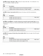
CFG Mask Timer Clock Selection Bits (CPS1, CPS0): Selects the clock source
for the CFG mask timer. (
φ
s = fosc/2)
Bit 1
Bit 0
CPS1
CPS0
Description
0
φ
s/1024
(Initial value)
0
1
φ
s/512
0
φ
s/256
1
1
φ
s/128
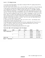
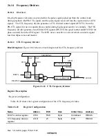
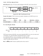
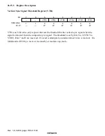
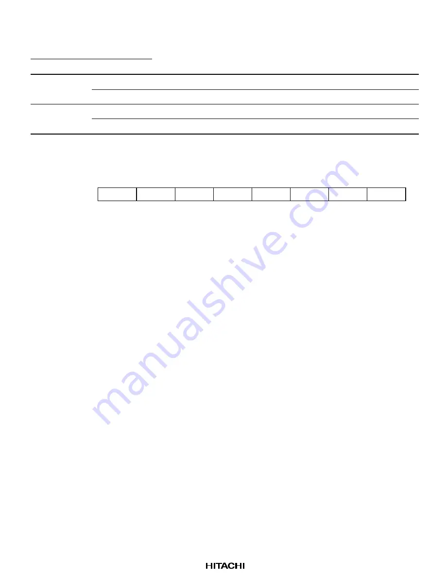
CFG Frequency Division Register 1 (CDIVR1)
0
0
1
0
W
2
0
W
3
4
0
W
5
0
6
7
—
—
W
W
CDV15
CDV14
0
W
CDV16
0
W
CDV13
CDV12
CDV11
CDV10
1
Bit :
Initial value :
R/W :
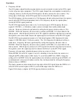
CDIVR1 is an 8-bit write-only register to set the division value. If a read is attempted, an
undetermined value is read out. Bit 7 is reserved.
The frequency division value is written in the reload register and the down counter at the same
time.
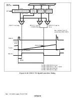
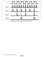
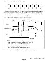
CFG's frequency is divided by N at its rising edge or both edges If the register value is 0, no
division operation is performed, and the DVCFG signal with the same input cycle with CFG
signal is output. The DVCFG signal is sent to the capstan speed error detector. It is initialized to
H'80 by a reset or in stand-by mode together with the capstan frequency division register and the
down counter.


