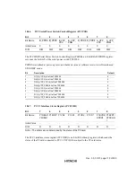
Rev. 3.0, 03/01, page 118 of 390
10.4.5
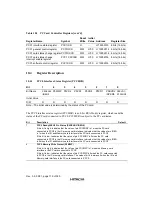
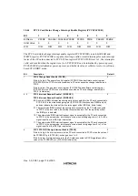
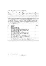
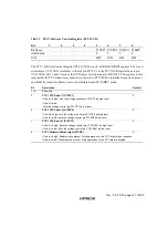
PCC0 Software Control Register (PCC0SCR)
Bit
7
6
5
4
3
2
1
0
Bit Name
-
-
-
6+'1
P0VPP1 P0VPP0 P0VCC1 P0SWP
Initial Value
0
0
0
0
0
0
0
0
R/W
-
-
-
R/W
R/W
R/W
R/W
R/W
The PCC0 Software Control Register (PCC0CSCR) is an 8-bit READ/WRITE register. The way it
controls pin VCC0SEL1 resembles to that of pin P0VCC0 in the PCC0GCR register does to pin
VCC0SEL0. Bits 2 and 3 serve as the VPP power selection input to MIC2563, and bit 4 is the
Shut-Down bit of the TPS2206. This register is also responsible for PC Card memory window
write protect. PCC0SCR is initialized at power-up reset, and holds its value at software reset or in
software-based STANDBY mode.
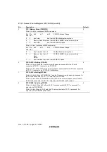
Bit
Description
Default
7 - 5
Reserved
0
4
D8 (SHDN) bit of the TPS2206
0
3
PCC0 VPP Select 1 (P0VPP1)
If this bit is high: set the voltage control pin P0VPP1 as high level
If this bit is low: set the voltage control pin P0VPP1 as low level
0
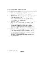
2
PCC0 VPP Select 0 (P0VPP0)
If the bit is high: set the voltage control pin P0VPP0 as high level
If this bit is low: set the voltage control pin P0VPP0 as low level
0
1
PCC0 VCC Select 1 (P0VCC1)
If this bit is high: Sets the voltage control pin VCC0SEL1 as high level.
If this bit is low: Sets the voltage control pin VCC0SEL1 as low level.
0
0
PCC0 Software Write Protect (P0SWP)
If this bit is high: Enables write protect. Write operations to the PC Card yield no response.
If this bit is low: Disables write protect. Write operations to the PC Card are allowed.
0
Summary of Contents for HD64465
Page 25: ...Rev 3 0 03 01 page 6 of 390 ...
Page 59: ...Rev 3 0 03 01 page 40 of 390 ...
Page 97: ...Rev 3 0 03 01 page 78 of 390 ...
Page 147: ...Rev 3 0 03 01 page 128 of 390 ...
Page 199: ...Rev 3 0 03 01 page 180 of 390 ...
Page 247: ...Rev 3 0 03 01 page 228 of 390 ...
Page 385: ...Rev 3 0 03 01 page 366 of 390 ...
Page 389: ...Rev 3 0 03 01 page 370 of 390 ...
Page 409: ...Rev 3 0 03 01 page 390 of 390 ...


