Rev. 3.0, 03/01, page 158 of 390
12.3
Serial Channel Register Description
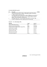
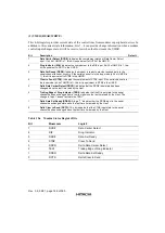
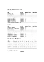
Table 12.1
Serial Channel Registers
Register
DLAB
*
Address
READ
WRITE
Data
0
Base+h0000
URBR (Receiver Buffer Register)
UTBR (Transmitter Buffer Register)
Control
0
X
X
X
1
1
Base+h0002
Base+h0004
Base+h0006
Base+h0008
Base+h0000
Base+h0002
UIER (Interrupt Enable Register)
UIIR (Interrupt identification Register)
ULCR (Line Control Register)
UMCR (Modem Control Register)
UDLL (Divisor Latch LSB)
UDLM (Divisor Latch MSB)
UIER
UFCR (FIFO Control Register)
ULCR
UMCR
UDLL
UDLM
Status
X
X
X
Base+h000A
Base+h000C
Base+h000E
ULSR (Line Status Register)
UMSR ( Modem Status Register)
USCR (Scratch Pad Register)
ULSR
UMSR
USCR
Notes: 1. DLAB
*
is bit 7 of the Line Control Register.
2. UART0 base address = H'10008000
12.3.1
Data Register
UTBR and URBR each hold from five to eight data bits. If the transmitted data is less than eight
bits, it aligns to the LSB. Either received or transmitted data is buffered by a shift register and is
latched first by a holding register. The bit 0 of any word is first received and transmitted.
(1) URBR (READ only)
This register receives and holds the entering data. It contains a non-accessible shift register which
converts the incoming serial data stream to a parallel 8 bit word.
(2) UTBR (WRITE only)
This register holds and transmits the data via a non-accessible shift register. It converts the
outgoing parallel data to a serial stream before transmission.
Summary of Contents for HD64465
Page 25: ...Rev 3 0 03 01 page 6 of 390 ...
Page 59: ...Rev 3 0 03 01 page 40 of 390 ...
Page 97: ...Rev 3 0 03 01 page 78 of 390 ...
Page 147: ...Rev 3 0 03 01 page 128 of 390 ...
Page 199: ...Rev 3 0 03 01 page 180 of 390 ...
Page 247: ...Rev 3 0 03 01 page 228 of 390 ...
Page 385: ...Rev 3 0 03 01 page 366 of 390 ...
Page 389: ...Rev 3 0 03 01 page 370 of 390 ...
Page 409: ...Rev 3 0 03 01 page 390 of 390 ...

