Rev. 3.0, 03/01, page 238 of 390
Data Transmit with Register
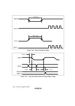
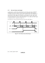
When data are transmitted via TXDR, data stored in TXDR are used as the transmitted data. When
data transmission starts in TXDR, TDEI is output. TERI is output when the next FX is received
before the transmitted data are written to TXDR.
Before 1
st
Data Transmit in Buffer Use Mode
In an AFE-interface module, it is defined that both transmit data buffers are empty when the TE bit
is 0. Consequently, data must be written to both of the transmit data buffers, and the TDE bit in
STR must be cleared before initiating the data transmit (before the TE bit is set to 1). Since the
TAB bit is 0 when they are empty, the TAB bit should be first set to 1 by the first clear operation,
and then cleared to 0 by the second clear operation.
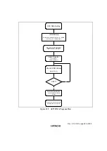
The following details how the whole procedure works:
1) 48 words of data are written to one transmit data buffer.
2) STR is read and 0 is written to bit 1.
3) Further 48 words of data are written to the other transmit data buffer.
4) STR is read and 0 is written to bit 1.
If the TDE bit is cleared without writing any data to transmit data buffers (only steps 2 and 4 in the
above procedure are performed), the output value cannot be guaranteed for the first 96 words of
data.
15.3.2
Data Receive
Data are received by setting the RE bit in CTR to 1.Received data can be stored in RXDR (receive
data register) or RXDB0/RXDB1 (receive data buffer 0 or 1), which is determined by the BUFD
bit in CTR.
Data Receive with Buffer
When data are to be received via RXDB0/RXDB1, the hardware will determine it will receive and
select the data in buffer 0 or buffer 1. At this moment, the CPU (SH3) can only access one buffer,
which is not used to receive data.
When the received data are completely stored in one buffer, a receive data full interrupt (RDFI) is
output. A receive data error interrupt (RERI) is output when a received data is pending while the
received data have been fully written in the two buffers.
When a buffer is used to receive data, RXDR is used as an AFE control data receive register, in
which data are stored and transmitted synchronously via the third FS (frame synchronous single)
after the HC bit is set to 1.
Summary of Contents for HD64465
Page 25: ...Rev 3 0 03 01 page 6 of 390 ...
Page 59: ...Rev 3 0 03 01 page 40 of 390 ...
Page 97: ...Rev 3 0 03 01 page 78 of 390 ...
Page 147: ...Rev 3 0 03 01 page 128 of 390 ...
Page 199: ...Rev 3 0 03 01 page 180 of 390 ...
Page 247: ...Rev 3 0 03 01 page 228 of 390 ...
Page 385: ...Rev 3 0 03 01 page 366 of 390 ...
Page 389: ...Rev 3 0 03 01 page 370 of 390 ...
Page 409: ...Rev 3 0 03 01 page 390 of 390 ...


