Page
Item
Description
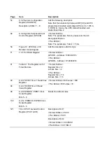
54
6.3.2 System Configuration
Register (SCONFR)
Description of Bits 11 - 8
Add the following description
Note that the relationship between HW[3:0] and CPU
programmed inserted wait states (IWS) is 2
≤
1 WS
≤
1+HW[3:0]. Hence, the CPU default inserted wait
states should be 2.
58
6.3.4 System Peripheral Clock
Control Register (SPCCR)
<Former Edition>
Note: The parameter, Twkst, please refer the AC
timing specification.
<This Edition>
Note: The parameter, Twkst = 15 ms
59
Figure 6.1 AFECK & LCK
Related Clock Diagram
Add the description ofACCLK pin
71
7.3.1 Port Data Register
<Former Edition>
GPCDR -- Address: 100004018h
<This Edition>
GPEDR -- Address: H’100004018
91
Table 9.1 The Register List of
Timer Module
<Former Edition>
Register Size = 2
Access Size = 2
<This Edition>
Register Size = 16
Access Size = 16
93
9.2.3 TRVR1:Timer 1 Read Vlue
Register
94
9.2.4 TRVR0:Timer 0 Read
Value Register
<Former Edition> R/W value = R/O
<This Edition> R/W value = R
99
9.2.9 PWM1CS: PWM1 Clock
Scale Register
Bits 5 - 0
102
9.2.12 PWM0CS: PWM0 Clock
Scale Register
Bits 5 - 0
Delete the default value
Description of bit 7
<Former Edition> PCC0
<This Edition> PCC1
121
10.4.8 PCC1 General Control
Register (PCC1GCR)
Description of bit 4
<Former Edition> VCC0SEL1
<This Edition> VCC1SEL0
Summary of Contents for HD64465
Page 25: ...Rev 3 0 03 01 page 6 of 390 ...
Page 59: ...Rev 3 0 03 01 page 40 of 390 ...
Page 97: ...Rev 3 0 03 01 page 78 of 390 ...
Page 147: ...Rev 3 0 03 01 page 128 of 390 ...
Page 199: ...Rev 3 0 03 01 page 180 of 390 ...
Page 247: ...Rev 3 0 03 01 page 228 of 390 ...
Page 385: ...Rev 3 0 03 01 page 366 of 390 ...
Page 389: ...Rev 3 0 03 01 page 370 of 390 ...
Page 409: ...Rev 3 0 03 01 page 390 of 390 ...


