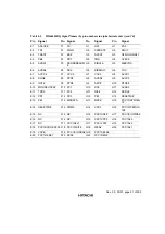
Rev. 3.0, 03/01, page 30 of 390
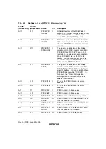
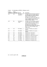
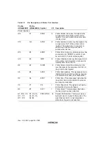
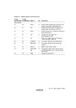
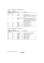
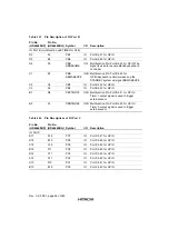
Table 4.6
Pin Descriptions of PCMCIA 1 Interface (cont’d)
Pin No.
(HD64465BP)
Pin No.
(HD64465BQ) Symbol
I/O
Description
G26
D20
PCC1BVD1/
STSCHG1#
I
The signal indicates the battery condition on
the PCC1 memory card. Both PCC1BVD1
and PCC1BVD2 are in high level when the
battery is in good condition. When
PCC1BVD1 is low, the PC card battery is no
longer serviceable and data are lost. For I/O
card, PCC1BVD1 is used as card status
change ( STSCHG ) function.
G25
E18
PCC1BVD2/
SPKR1
I
The signal indicates the battery condition on
the PCC1 memory card. Both PCC1BVD1
and PCC1BVD2 are in high level when the
battery is in good condition. When
PCC1BVD2 is low while PCC1BVD1 is in
high level, the PC card battery is in a warning
state. For I/O card, PCC1BVD2 is used
SPKR function.
F26
C20
PCC1CD1#
I
Provided for PCMCIA card 1 insertion
detection
F25
G15
PCC1CD2#
I
Provided for PCMCIA card 1 insertion
detection
G24
G17
PCC1VS1#
I
PCMCIA card 1 Voltage sense
G23
D19
PCC1VS2#
I
PCMCIA card 1 Voltage sense
K26
G20
PCC1REG#
O
PCMCIA card 1 attribute memory select
E25
F17
VCC1SEL1
O
PCMCIA card 1 VCC power control
E26
C19
VCC1SEL0
O
PCMCIA card 1 VCC power control
F23
D18
VCC1VPP1
O
PCMCIA card 1 VPP power control
F24
G16
VCC1VPP0
O
PCMCIA card 1 VPP power control
Summary of Contents for HD64465
Page 25: ...Rev 3 0 03 01 page 6 of 390 ...
Page 59: ...Rev 3 0 03 01 page 40 of 390 ...
Page 97: ...Rev 3 0 03 01 page 78 of 390 ...
Page 147: ...Rev 3 0 03 01 page 128 of 390 ...
Page 199: ...Rev 3 0 03 01 page 180 of 390 ...
Page 247: ...Rev 3 0 03 01 page 228 of 390 ...
Page 385: ...Rev 3 0 03 01 page 366 of 390 ...
Page 389: ...Rev 3 0 03 01 page 370 of 390 ...
Page 409: ...Rev 3 0 03 01 page 390 of 390 ...

