13. 512K CMOS Serial Flash – MX25L512
13.1. General Description
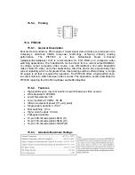
The MX25L512 is a CMOS 524,288 bit serial Flash memory, which is configured as
65,536 x 8 internally. The MX25L512 feature a serial peripheral interface and software
protocol allowing operation on a simple 3-wire bus. The three bus signals are a clock
input (SCLK), a serial data input (SI), and a serial data output (SO). SPI access to the
device is enabled by CS# input. The MX25L512 provide sequential read operation on
whole chip. After program/erase command is issued, auto program/ erase algorithms
which program/ erase and verify the specified page or sector/block locations will be
executed. Program command is executed on page (256 bytes) basis, and erase
command is executes on chip or sector (4K-bytes). To provide user with ease of
interface, a status register is included to indicate the status of the chip. The status read
command can be issued to detect completion status of a program or erase operation via
WIP bit. When the device is not in operation and CS# is high, it is put in standby mode
and draws less than 10uA DC current. The MX25L512 utilize MXIC's proprietary
memory cell, which reliably stores memory contents even after 100,000 program and
erase cycles.
13.2. Features
GENERAL
x
Serial Peripheral Interface (SPI) compatible -- Mode 0 and Mode 3
x
524,288 x 1 bit structure
x
16 Equal Sectors with 4K byte each
x
Any Sector can be erased individually
x
Single Power Supply Operation
x
2.7 to 3.6 volt for read, erase, and program operations
x
Latch-up protected to 100mA from -1V to Vcc +1V
x
Low Vcc write inhibit is from 1.5V to 2.5V
PERFORMANCE
x
High Performance
x
Fast access time: 85MHz serial clock (15pF + 1TTL Load) and 66MHz serial
clock (30pF + 1TTL Load)
x
Fast program time: 1.4ms(typ.) and 5ms(max.)/page (256-byte per page)
x
Fast erase time: 60ms(typ.) and 120ms(max.)/sector (4K-byte per sector) ;
1s(typ.) and 2s(max.)/chip(512Kb)
x
Low Power Consumption
x
Low active read current: 12mA(max.) at 85MHz, 8mA(max.) at 66MHz and
4mA(max.) at 33MHz
x
Low active programming current: 15mA (max.)
x
Low active erase current: 15mA (max.)
x
Low standby current: 10uA (max.)
x
Deep power-down mode 1uA (typical)
x
Minimum 100,000 erase/program cycles
Summary of Contents for L26HP03E
Page 6: ......
Page 10: ...3 4 2 Operating Specifications 3 5 Pinning ...
Page 14: ...6 4 Pinning Configuration Pins ...
Page 27: ...12 4 Pinning ...
Page 34: ......
Page 57: ...15 18 4 Pinning ...
Page 75: ......
Page 76: ...18 2 Power Management ...
Page 77: ...18 3 Integrated DVB T Receiver Block Diagram ...
Page 78: ...18 4 MSTAR Block Diagram ...

