background image

S10 Series SIO Driver   

GP-Pro EX Device/PLC Connection Manual

36

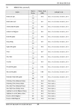
Timer (Elapsed Value)

-

TC000 - TC1FF

Timer (Setup Value)

-

TS000 - TS1FF

One-shot Timer (Elapsed Value)

-

UC000 - UC0FF

One-shot Timer (Setup Value)

-

US000 - US0FF

Counter (Elapsed Value)

-

CC000 - CC0FF

Counter (Setup Value)

-

CS000 - CS0FF

Work Register

-

FW000 - FWBFF

Data Register

-

DW000 - DWFFF

Work Register

LB0000 - LBFFFF

LBW0000 - LBWFFF0

Work Register for Ladder 
Converter

LR0000 - LR0FFF

LRW0000 - LRW0FF0

Work Register for Ladder 
Converter (Edge)

LV0000 - LV0FFF

LVW0000 - LVW0FF0

Work Register for Word

-

LWW0000 - LWWFFFF

Work Register for Long Word

-

LLL0000 - LLL1FFF

*5

Work Register for Floating 
Point

-

LF0000 - LF1FFF

*5


*6

Work Register for Word 
(Save during power OFF) 

-

LXW0000 - LXW3FFF

Work Register for Long Word
(Save during power OFF) 

-

LML0000 - LML1FFF

*5

Work Register for Floating 
Point (Save during power OFF)

-

LG0000 - LG1FFF

*5


*6

Direct Memory Address

*7

-

DM00000000 - 

DMFFFFFFFE

*1

According to External Device specification, the highest bit is "0" and the lowest bit is "15". When the highest                  
bit turns ON, that bit is considered the highest and "32768" is written to that word.

Ex. When writing bit from the Display is "X000(ON)," the External Device's bit device "X000" turns ON.


 At this time the Display and External Device word device "XW000" become "32768(0x8000)".

*2

The higher and lower bit order will be reversed. When EW400 is turned ON, E40F will be turned ON on the                    
External Device.

*3

Data cannot be written.

*4

If the CPU version is prior to Ver.1, the bit address becomes "T000 to T1FF" and the word address becomes                   
"TW000 to TW1F0."

*5

A 32-bit device.

*6

A float decimal point device (32 bits).

*7

Used to access the memory address of the External Device.

Device

Bit Address

Word Address

32 bits

Remarks

Summary of Contents for S10 Series

Page 1: ...ries SIO Driver 1 System Configuration 3 2 Selection of External Device 7 3 Example of Communication Setting 8 4 Setup Items 18 5 Cable Diagram 23 6 Supported Device 35 7 Device Code and Address Code 44 8 Error Messages 53 ...

Page 2: ...ice Select a model series of the External Device to be connected and connection method 2 Selection of External Device page 7 3 Example of Communication Settings This section shows setting examples for communicating between the Display and the External Device 3 Example of Communication Setting page 8 4 Setup Items This section describes communication setup items on the Display Set communication set...

Page 3: ... 29 LQE560 CN2 RS232C Setting Example 3 page 10 Cable Diagram 2 page 29 LQE565 CN1 RS422 485 4wire Setting Example 4 page 11 Cable Diagram 1 page 23 LQE565 CN2 RS422 485 4wire Setting Example 5 page 12 Cable Diagram 1 page 23 HIDIC S10α 2α LWP000 2 2αE LWP040 2 2αH LWP070 2 2 Connect to the CPU Module s HOST LINK COMPUTER LINK Input Output Terminal Upper Calculation I F Terminal Block on CPU Unit ...

Page 4: ...COM1 1 COM2 2 COM2 2 COM2 2 PS4000 3 3 When making communication between an External Device and COM port on the Expansion slot only RS 232C is supported However ER DTR CTS control cannot be executed because of the specification of COM port For connection with External Device use user created cables and disable Pin Nos 1 4 6 and 9 Please refer to the IPC manual for details of pin layout COM1 COM2 P...

Page 5: ...ch The BOX Atom has not a switch to set the RS 232C RS 422 485 mode Use the BIOS for the setting 8 For the connection with the External Device on the user created cable read as if the connector on the Display side is a M12 A coding 8 pin socket The pin assignment is the same as described in the cable diagram For the M12 A coding connector use PFXZPSCNM122 DIP Switch Setting Description 1 OFF 1 1 W...

Page 6: ...F Short circuit of SDA TXA and RDA RXA Not available 8 OFF Short circuit of SDB TXB and RDB RXB Not available 9 OFF RS RTS Auto control mode Disabled 10 OFF DIP Switch Setting Description 1 OFF Reserved always OFF 2 ON SIO type RS 422 485 3 ON 4 OFF Output mode of SD TXD data Always output 5 OFF Terminal resistance 220Ω insertion to SD TXD None 6 OFF Terminal resistance 220Ω insertion to RD RXD No...

Page 7: ... the External Device you are connecting is supported by S10 Series SIO 1 System Configuration page 3 Port Select the Display port to be connected to the External Device Use System Area Check this option to synchronize the system data area of the Display and the device memory of the External Device When synchronized you can use the External Device s ladder program to switch the display or display t...

Page 8: ... Setting Example 1 Settings of GP Pro EX Communication Settings To display the setup screen from the Project menu point to System Settings and select Device PLC Device Setting To display the Individual Device Settings dialog box from Device Specific Settings in the Device PLC window select the external device and click Settings Settings of External Device Communication setting of External Device i...

Page 9: ...C Device Setting To display the Individual Device Settings dialog box from Device Specific Settings in the Device PLC window select the external device and click Settings Settings of External Device Communication setting of External Device is fixed No setting is required Rotary switch of External Device needs to be set depending on the channel in use Set as shown in the table below Channel in use ...

Page 10: ...C Device Setting To display the Individual Device Settings dialog box from Device Specific Settings in the Device PLC window select the external device and click Settings Settings of External Device Communication setting of External Device is fixed No setting is required Rotary switch of External Device needs to be set depending on the channel in use Set as shown in the table below Channel in use ...

Page 11: ...C Device Setting To display the Individual Device Settings dialog box from Device Specific Settings in the Device PLC window select the external device and click Settings Settings of External Device Communication setting of External Device is fixed No setting is required Rotary switch of External Device needs to be set depending on the channel in use Set as shown in the table below Channel in use ...

Page 12: ...C Device Setting To display the Individual Device Settings dialog box from Device Specific Settings in the Device PLC window select the external device and click Settings Settings of External Device Communication setting of External Device is fixed No setting is required Rotary switch of External Device needs to be set depending on the channel in use Set as shown in the table below Channel in use ...

Page 13: ...t Device PLC Device Setting To display the Individual Device Settings dialog box from Device Specific Settings in the Device PLC window select the external device and click Settings Settings of External Device Communication setting of External Device is fixed No setting is required Communication speed differs depending on the External Device in use Please refer to the manual of the External Device...

Page 14: ...C Device Setting To display the Individual Device Settings dialog box from Device Specific Settings in the Device PLC window select the external device and click Settings Settings of External Device Communication setting of External Device is fixed No setting is required Rotary switch of External Device needs to be set depending on the channel in use Set as shown in the table below Channel in use ...

Page 15: ...C Device Setting To display the Individual Device Settings dialog box from Device Specific Settings in the Device PLC window select the external device and click Settings Settings of External Device Communication setting of External Device is fixed No setting is required Rotary switch of External Device needs to be set depending on the channel in use Set as shown in the table below Channel in use ...

Page 16: ...C Device Setting To display the Individual Device Settings dialog box from Device Specific Settings in the Device PLC window select the external device and click Settings Settings of External Device Communication setting of External Device is fixed No setting is required Rotary switch of External Device needs to be set depending on the channel in use Set as shown in the table below Channel in use ...

Page 17: ...LC Device Setting To display the Individual Device Settings dialog box from Device Specific Settings in the Device PLC window select the external device and click Settings Settings of External Device Communication setting of External Device is fixed No setting is required Rotary switch of External Device needs to be set depending on the channel in use Set as shown in the table below Channel in use...

Page 18: ...nal Device Speed Select the communication speed between the External Device and the Display Data Length Select data length Parity Select how to check parity Stop Bit Select stop bit length Flow Control Select the communication control method to prevent overflow of transmission and reception data Timeout Use an integer from 1 to 127 to enter the time s for which the Display waits for the response f...

Page 19: ...t RS232C for SIO type When you connect to IPC you need to use the IPC change switch to change RI 5V Please refer to the manual of IPC for details Refer to the GP Pro EX Reference Manual for Indirect Device Cf GP Pro EX Reference Manual Changing the Device PLC at Runtime Indirect Device Setup Items Setup Description Series Select the series of the External Device Expanded Memory Address HEX Enter t...

Page 20: ...ease refer to the Reference manual for details Setup Items Setup Description SIO Type Select the SIO type to communicate with the External Device In the communication setting confirm the serial interface specifications of the Display and set SIO Type correctly If you select the SIO type the serial interface does not support we cannot guarantee the operation Please refer to the manual of the Displa...

Page 21: ...f no response from the External Device use an integer from 0 to 255 to enter how many times the Display retransmits the command Wait To Send ms Use an integer from 0 to 255 to enter standby time ms for the Display from receiving packets to transmitting next commands Setup Items Setup Description Device PLC Name Select the External Device to set Device name is a title of the External Device set wit...

Page 22: ...e you want to set from the displayed list and touch Option Setup Items Setup Description RI VCC You can switch RI VCC of the 9th pin when you select RS232C for SIO type When you connect to IPC you need to use the IPC change switch to change RI 5V Please refer to the manual of IPC for details GP 4100 series GP 4 01TM and GP Rear Module do not have the Option setting in the offline mode ...

Page 23: ...ule COM1 ST 2 COM2 LT3000 COM1 IPC 3 1 All GP models except AGP 3302B 2 All ST models except AST 3211A and AST 3302B 3 Available to use only the COM ports which can communicate in RS422 485 4 wire Except PE 4000B PS5000 IPC COM Port page 4 1A COM port conversion adapter by Pro face CA3 ADPCOM 01 Connector terminal block conversion adapter by Pro face CA3 ADPTRM 01 Your own cable Cable length 500m ...

Page 24: ... and GP 4 03T 6 Except SP 5B00 7 When using a Terminal Block Conversion Adapter CA3 ADPTRM 01 instead of the RS 422 Terminal Block Conversion Adapter refer to Cable Diagram 1A 8 Available to use only the COM ports which can communicate in RS422 485 4 wire IPC COM Port page 4 Termination resistance 100Ω between RD H and RD L is incorporated in the LPU module and LQE565 of the External Device ...

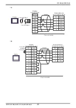
Page 25: ...SDB SG FG Signal name Signal name Pin Display Terminal block Your own cable CA3 ADPTRM 01 CA3 ADPCOM 01 Display Shield RDA RDB SDA SDB SG ERA CSA ERB CSB FG SD H SD L RD H RD L SG 1 2 3 7 5 4 8 9 6 Shell Signal name Pin Display D Sub 9pin socket 3 4 2 1 5 Signal name Pin External Device D Sub 9pin socket Termination resistance 100Ω 1 2W Your own cable Display ...

Page 26: ...ignal name TRM RDA RDB SDA SDB SG FG Signal name Pin Display Terminal block Your own cable CA3 ADPTRM 01 CA4 ADPONL 01 Display Shield TRMRX RDA RDB SDA SDB SG TRMTX FG SD H SD L RD H RD L SG 1 2 7 3 8 5 9 Shell Signal name Pin Display D Sub 9pin plug 3 4 2 1 5 Signal name Pin External Device D Sub 9pin socket CA4 ADPONL 01 Display Your own cable ...

Page 27: ...RDA RDB SDA SDB SG FG Signal name Signal name Pin Display Terminal block Your own cable PFXZCBADTM1 Display Shield Rx Rx Tx Tx GND NC NC NC NC FG SD H SD L RD H RD L SG 3 4 2 1 5 7 8 9 6 Shell Signal name Pin Display D Sub 9pin socket 3 4 2 1 5 Signal name Pin External Device D Sub 9pin socket Termination resistance 100Ω 1 2W Your own cable Display ...

Page 28: ...et the value of the DIP Switch on the rear of the Display as shown in the table below DIP Switch No Set Value 1 OFF 2 OFF 3 ON 4 ON Shield RDA RDB SDA SDB SG ERA CSA ERB CSB SD H SD L RD H RD L SG Signal name Display Terminal block 3 4 2 1 5 Signal name Pin External Device D Sub 9pin socket Termination resistance 1 Your own cable Display ...

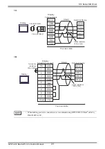
Page 29: ... RS232C IPC COM Port page 4 2A Your own cable Cable length 15m or less GP 4115T COM1 GP 4115T3 COM1 2B Your own cable Cable length 15m or less Shield RD RXD SD TXD ER DTR SG RS RTS CS CTS FG SD RD DR SG CD RS CS 2 3 4 5 7 8 Shell Signal name Pin Display D Sub 9pin socket 3 2 6 5 1 7 8 Signal name Pin External Device D Sub 9pin socket Your own cable Display Shield RD RXD SD TXD ER DTR SG RS RTS CS ...

Page 30: ...lock conversion adapter by Pro face CA3 ADPTRM 01 Your own cable Please refer to the manual of the External Device for cable length 3D Online adapter by Pro face CA4 ADPONL 01 Your own cable GP 4116T COM1 3G Your own cable Please refer to the manual of the External Device for cable length GP4000 5 COM2 GP 4201T COM1 SP5000 6 COM1 2 SP 5B00 COM2 5 All GP4000 models except GP 4100 Series GP 4 01TM G...

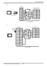
Page 31: ...e Shield Signal name TRM RDA RDB SDA SDB SG FG Signal name Display Terminal block Your own cable Series resistance 100Ω 1 2W CA3 ADPTRM 01 CA3 ADPCOM 01 Display RDA RDB SDA SDB SG ERA CSA ERB CSB FG 1 2 3 7 5 4 8 9 6 Shell Signal name Pin Display D Sub 9pin socket Termination resistance 100Ω 1 2W Your own cable UTX H UTX L URX H URX L External Device Shield Signal name Series resistance 100Ω 1 2W ...

Page 32: ...DA SDB SG FG Signal name Display Terminal block Your own cable Series resistance 100Ω 1 2W CA3 ADPTRM 01 CA4 ADPONL 01 Display TRMRX RDA RDB SDA SDB TRMTX SG FG 1 2 7 3 8 9 5 Shell Signal name Pin Display D Sub 9pin plug CA4 ADPONL 01 Display Your own cable UTX H UTX L URX H URX L External Device Shield Signal name Series resistance 100Ω 1 2W ...

Page 33: ...ernal Device Shield Signal name TRM RDA RDB SDA SDB SG FG Signal name Display Terminal block Your own cable Series resistance 100Ω 1 2W PFXZCBADTM1 Display Rx Rx Tx Tx GND NC NC NC NC FG 3 4 2 1 5 7 8 9 6 Shell Signal name Pin Display D Sub 9pin socket Termination resistance 100Ω 1 2W Your own cable UTX H UTX L URX H URX L External Device Shield Signal name Series resistance 100Ω 1 2W Display ...

Page 34: ...he Display as shown in the table below When making your own connections we recommend using KPEV SB 3P 0 5mm2 cable by Hitachi Cable Ltd DIP Switch No Set Value 1 OFF 2 OFF 3 ON 4 ON RDA RDB SDA SDB SG ERA CSA ERB CSB Signal name Display Terminal block Termination resistance 1 Your own cable UTX H UTX L URX H URX L External Device Shield Signal name Series resistance 100Ω 1 2W Display ...

Page 35: ...nal Input X000 XFFF XW000 XWFF0 1 External Output Y000 YFFF YW000 YWFF0 1 Internal Register R000 RFFF RW000 RWFF0 1 Global Link Register G000 GFFF GW000 GWFF0 1 Event Register E000 E3FF EW000 EW3F0 1 Event Register EW400 EWFFF EW400 EWFF0 1 2 Keep Relay K000 KFFF KW000 KWFF0 1 System Register S000 SBFF SW000 SWBF0 1 3 On delay Timer T000 T7FF TW000 TW7F0 1 4 One shot Timer U000 U0FF UW000 UW0F0 1 ...

Page 36: ...ower OFF LML0000 LML1FFF 5 Work Register for Floating Point Save during power OFF LG0000 LG1FFF 5 6 Direct Memory Address 7 DM00000000 DMFFFFFFFE 1 According to External Device specification the highest bit is 0 and the lowest bit is 15 When the highest bit turns ON that bit is considered the highest and 32768 is written to that word Ex When writing bit from the Display is X000 ON the External Dev...

Page 37: ...e system uses If you conduct it an error may occur For details concerning the address refer to the manual attached to the External Device Please refer to the GP Pro EX Reference Manual for system data area Cf GP Pro EX Reference Manual LS Area Direct Access Method Area Please refer to the precautions on manual notation for icons in the table Manual Symbols and Terminology ...

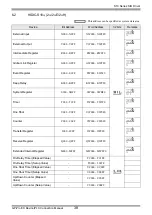
Page 38: ...r E000 E3FF EW000 EW3F0 1 Keep Relay K000 KFFF KW000 KWFF0 1 System Register S000 SBFF SW000 SWBF0 1 2 Timer T000 T1FF TW000 TW1F0 1 One Shot U000 U0FF UW000 UW0F0 1 Counter C000 C0FF CW000 CW0F0 1 Transfer Register J000 JFFF JW000 JWFF0 1 Receive Register Q000 QFFF QW000 QWFF0 1 Extended Internal Register M000 MFFF MW000 MWFF0 1 On Delay Timer Elapsed Value TC000 TC1FF On Delay Timer Setup Value ...

Page 39: ...s 180000 and the Device Address is MS1FF Then the absolute address in External Device Access Address is 180000 100000 3FE 2803FE 4 Used to access the memory address of the External Device When you access the External Device using the Direct Memory Address do not access the memory address that the system uses If you conduct it an error may occur For details concerning the address refer to the manua...

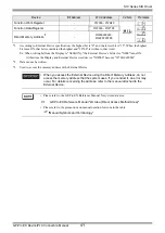
Page 40: ...E000 E3FF EW000 EW3F0 1 Keep Relay K000 KFFF KW000 KWFF0 1 System Register S000 SBFF SW000 SWBF0 1 2 Timer T000 T1FF TW000 TW1F0 1 One Shot U000 U0FF UW000 UW0F0 1 Counter C000 C0FF CW000 CW0F0 1 Transfer Register J000 JFFF JW000 JWFF0 1 Receive Register Q000 QFFF QW000 QWFF0 1 Extended Internal Register M000 MFFF MW000 MWFF0 1 On Delay Timer Elapsed Value TC000 TC1FF On Delay Timer Setup Value TS...

Page 41: ...e Display and External Device word device XW000 become 32768 0x8000 2 Data cannot be written 3 Used to access the memory address of the External Device When you access the External Device using the Direct Memory Address do not access the memory address that the system uses If you conduct it an error may occur For details concerning the address refer to the manual attached to the External Device Pl...

Page 42: ...r EW400 EWFFF EW400 EWFF0 1 2 Keep Relay K000 KFFF KW000 KWFF0 1 System Register S000 SBFF SW000 SWBF0 1 3 On Delay Timer T000 T1FF TW000 TW1F0 1 One Shot Timer U000 U0FF UW000 UW0F0 1 Up Down Counter C000 C0FF CW000 CW0F0 1 Transfer Register J000 JFFF JW000 JWFF0 1 Receive Register Q000 QFFF QW000 QWFF0 1 Extended Internal Register M000 MFFF MW000 MWFF0 1 On Delay Timer Elapsed Value TC000 TC1FF ...

Page 43: ... in External Device 1 2 3 Ex When the Top Address is 180000 and the Device Address is MS1FF Then the absolute address in External Device Access Address is 180000 100000 3FE 2803FE 5 Used to access the memory address of the External Device When you access the External Device using the Direct Memory Address do not access the memory address that the system uses If you conduct it an error may occur Fo...

Page 44: ...0 GW Event Register E 0084 Value of word address divided by 0x10 EW Event Register EW 0091 Value of word address divided by 0x10 EW Keep Relay K 0085 Value of word address divided by 0x10 KW System Register S 0086 Value of word address divided by 0x10 SW On delay Timer T 0087 Value of word address divided by 0x10 TW One shot Timer U 0088 Value of word address divided by 0x10 UW Up Down Counter C 0...

Page 45: ...rk Register for Word LWW 0002 Word Address Work Register for Long Word LLL 0003 Word Address Work Register for Floating Point LF 0066 Word Address Work Register for Word Save during power OFF LXW 0004 Word Address Work Register for Long Word Save during power OFF LML 0005 Word Address Work Register for Floating Point Save during power OFF LG 0067 Word Address Direct Memory Address DM00000000 DM0FF...

Page 46: ...ss DM90000000 DM9FFFFFFE 0010 Direct Memory Address DMA0000000 DMAFFFFFFE 0011 Direct Memory Address DMB0000000 DMBFFFFFFE 0012 Direct Memory Address DMC0000000 DMCFFFFFFE 0013 Direct Memory Address DMD0000000 DMDFFFFFFE 0014 Direct Memory Address DME0000000 DMEFFFFFFE 0015 Direct Memory Address DMF0000000 DMFFFFFFFE 0016 Device Device Name Device Code HEX Address Code ...

Page 47: ...mer T 0087 Value of word address divided by 0x10 TW One Shot U 0088 Value of word address divided by 0x10 UW Counter C 0089 Value of word address divided by 0x10 CW Transfer Register J 008A Value of word address divided by 0x10 JW Receive Register Q 008B Value of word address divided by 0x10 QW Extended Internal Register M 008C Value of word address divided by 0x10 MW On Delay Timer Elapsed Value ...

Page 48: ...ss DM50000000 DM5FFFFFFE 000C Direct Memory Address DM60000000 DM6FFFFFFE 000D Direct Memory Address DM70000000 DM7FFFFFFE 000E Direct Memory Address DM80000000 DM8FFFFFFE 000F Direct Memory Address DM90000000 DM9FFFFFFE 0010 Direct Memory Address DMA0000000 DMAFFFFFFE 0011 Direct Memory Address DMB0000000 DMBFFFFFFE 0012 Direct Memory Address DMC0000000 DMCFFFFFFE 0013 Direct Memory Address DMD00...

Page 49: ...ided by 0x10 SW Timer T 0087 Value of word address divided by 0x10 TW One Shot U 0088 Value of word address divided by 0x10 UW Counter C 0089 Value of word address divided by 0x10 CW Transfer Register J 008A Value of word address divided by 0x10 JW Receive Register Q 008B Value of word address divided by 0x10 QW Extended Internal Register M 008C Value of word address divided by 0x10 MW On Delay Ti...

Page 50: ...ss DM50000000 DM5FFFFFFE 000C Direct Memory Address DM60000000 DM6FFFFFFE 000D Direct Memory Address DM70000000 DM7FFFFFFE 000E Direct Memory Address DM80000000 DM8FFFFFFE 000F Direct Memory Address DM90000000 DM9FFFFFFE 0010 Direct Memory Address DMA0000000 DMAFFFFFFE 0011 Direct Memory Address DMB0000000 DMBFFFFFFE 0012 Direct Memory Address DMC0000000 DMCFFFFFFE 0013 Direct Memory Address DMD00...

Page 51: ...m Register S 0086 Value of word address divided by 0x10 SW On Delay Timer T 0087 Value of word address divided by 0x10 TW One Shot Timer U 0088 Value of word address divided by 0x10 UW Up Down Counter C 0089 Value of word address divided by 0x10 CW Transfer Register J 008A Value of word address divided by 0x10 JW Receive Register Q 008B Value of word address divided by 0x10 QW Extended Internal Re...

Page 52: ...0 DM4FFFFFFE 000B Direct Memory Address DM50000000 DM5FFFFFFE 000C Direct Memory Address DM60000000 DM6FFFFFFE 000D Direct Memory Address DM70000000 DM7FFFFFFE 000E Direct Memory Address DM80000000 DM8FFFFFFE 000F Direct Memory Address DM90000000 DM9FFFFFFE 0010 Direct Memory Address DMA0000000 DMAFFFFFFE 0011 Direct Memory Address DMB0000000 DMBFFFFFFE 0012 Direct Memory Address DMC0000000 DMCFFF...

Page 53: ...f the External Device set with GP Pro EX Initial value PLC1 Error Message Displays messages related to the error that has occurred Error Occurrence Area Displays IP address or device address of the External Device where an error occurs or error codes received from the External Device IP address is displayed such as IP address Decimal MAC address Hex Device address is displayed as Address Device ad...

Reviews: