3 INDIVIDUAL SPECIFICATIONS
3-83
FG
Channel 0
E
ECM
A/D
LQA310
Internal circuit
LQA301
Internal circuit
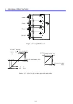
E: Input voltage
ECM: Inter-common voltage
SV0
C0
SHD
SV1
C1
SHD
SV2
C2
SHD
SV3
C3
SHD
Channel 1
Channel 2
Channel 3
Control circuit
Control circuit
Amplifier
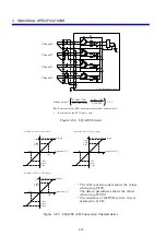
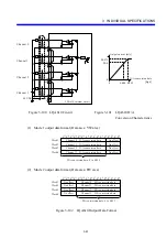
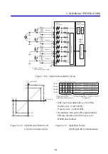
Figure 3-104 LQA301 and LQA310 Circuit
5.0
5.12
Input voltage
[V]
A/D conversion data
[digit]
2,000
2,047
-5.0
-5.12
-2,000
-2,048
0
2
15
2
14
2
13
2
12
2
11
2
10
2
0
S
S
S
S
S
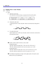
Channel 0 A/D conversion data
S
S
S
S
S
Channel 1 A/D conversion data
S
S
S
S
S
Channel 2 A/D conversion data
S
S
S
S
S
Channel 3 A/D conversion data
Word 1
Word 2
Word 3
Word 4
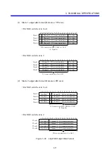
A/D conversion data: -2,048 to +2,047
(S: Sign bit)
The content of the
sign bit is reflected here.
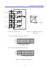
Figure 3-105 LQA301 and LQA310 A/D
Figure 3-106 Input Data Format
Conversion
Characteristics
(Data area: EW area)
y
A/D conversion data in times of overflow
Positive side: +2,047 (H7FF)
Negative side: -2,048 (H800)
y
Immediately after power ON (approximately
800 ms), the data in the EW area is set to H8000
(invalid data).
Summary of Contents for S10mini LQS070
Page 1: ......
Page 2: ......
Page 19: ...This Page Intentionally Left Blank ...
Page 30: ...1 BEFORE USE ...
Page 37: ...This Page Intentionally Left Blank ...
Page 38: ...2 KINDS AND SPECIFICATIONS OF I O MODULES ...
Page 57: ...This Page Intentionally Left Blank ...
Page 58: ...3 INDIVIDUAL SPECIFICATIONS ...
Page 143: ...This Page Intentionally Left Blank ...
Page 144: ...4 HANDLING ...
Page 179: ...This Page Intentionally Left Blank ...
Page 180: ...5 HANDLING I O DATA ON J NET ...
Page 186: ...6 HANDLING I O DATA ON D Station ...
Page 191: ...This Page Intentionally Left Blank ...
Page 192: ...7 MAINTENANCE ...

