background image

2-7

GB

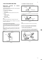
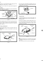
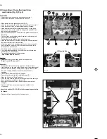
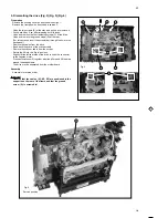
5. Dismantling the drive (Fig. 3)(Fig. 5)(Fig. 6)

Preparation

Remove the housing cover as described in section 1.
Remove the front panel as described in section 3.

- Undo the two screws (B) of the stay and pull it up to remove it.
- Push back lift by 5 cm after releasing both lift stops.
- Undo and remove the four fastening screws (C) of the drive.
- Undo and remove the ground screw (D) at the rear.

(For this purpose, insert the screwdriver through the hole in the
back panel).

- Remove the cables from the drive.
- Bend back the guard of the scanner cable.
- Remove the scanner cable from the socket.
- Return the lift into the ”Eject” position.
- Slightly lift the left rear side of the drive to undo the connector

to the capstan motor.

- Press both catches (S) together with fine pliers and lift the drive

around the snapholders.

- The drive may be separated from the motherboard.

Assembly

Assemble in reverse order.

Important

Observe that the cables  (K1; K2; K3) are positioned in the
supports on the rear of the frame and that the ground
screw (D) is screwed in!

Fig. 6

S

C

C

C

C

ä

ä

ä

D

S

Fig. 5

ä

D

Service position

Summary of Contents for VTFX940EUKN

Page 1: ...ffnen des Gehäuses hat der Service Ingenieur die Sicherheitshinweise und Hinweise zur Produktsicherheit in diesem Wartungshandbuch zu lesen Data contained within this Service manual is subject to alteration for improvement Les données fournies dans le présent manuel d entretien peuvent faire l objet de modifications en vue de perfectionner le produit Die in diesem War tungshandbuch enthaltenen Spe...

Page 2: ...uswechselbar gegen die Bauteile in dem Gerät ungeachtet der etwaigen Typenbezeichungen Avertissements Les normes de sécurité exigent qu aprés réparation I appareil soit remis dans son état d origine et que soient utilisées les piéces de rechange identiques à celles spécifiées Les composants de sécurité sont marqués Tout les IC et beaucoup d autres semi conducteurs sont sensibles aux décharger stat...

Page 3: ...tante l eventuale denominazione di modelli Avisos Las instrucciones de seguridad exigen que después de la reparación el aparato se encuentre en el estado original y que las piezas de repuesto utilizadas para la reparación sean idénticas a las originales Los componentes de seguridad estan marcados con Todos los IC y semiconductores son sensibles a descargas electrostáticas ESD Un tratamiento no con...

Page 4: ...order the production code on the type plate is increased by one E g 37 becomes 38 In the case of an important modification to the service documentation the evolution code on the type plate is increased by one E g AA becomes AB 220 240 V 220 240 V S AA 50Hz 50Hz MADE IN EUROPE MADE IN EUROPE MODEL NO MODEL NO AAA BBB CCC DDD EEE FFF GGG PROD NO PROD NO VR110 02 VN 37 0015 123456 VN 37 123456 SHOWVI...

Page 5: ...esolución video Risoluzione video 240 lines Audio Audio Audio SP Linear Audio 80Hz 10kHz 6 dB Audio LP Linear Audio 80Hz 5kHz 6 dB Stereo FM Audio 20Hz 20kHz 3dB F Euroconnector AV1 SCART plug 1 Connection to TV monitor projection TV Pin 1 ARO audio right out 500 mVrms 3 dB Rout 1 kOhm Pin 2 ARI audio right in 0 2 Vrms to 2Vrms Rin 10 kOhm Pin 3 ALO audio left out 500 mVrms 3 dB Rout 1 kOhm Pin 6 ...

Page 6: ......

Page 7: ...heat to both electrodes When the solder on both electrodes has melted remove leadless component with a twisting motion Note a Do not attempt to lift the component off the board until the component is completely disconnected from the board with a twisting motion b Be careful not to break the copper foil on the printed circuit board Fig 2 1 3 Installation of leadless components a Presolder the conta...

Page 8: ...on solder wire iron wire while heating the pins using a fine tip soldering iron or a hot air blower Fig 2 7 Using iron wire a Use unsoldering braid to remove the solder from all pins of the Flat Pack IC Apply solder flux to all pins of the Flat Pack IC to allow easy removal b Affix the wire to workbench or solid mounting point see Fig 2 8 c Pull up the wire as the solder melts in order to lift the...

Page 9: ...he Flat Pack IC indicates pin 1 Make sure this mark matches the 1 on the P C B when positioning for installation Then pre solder the four corners of the Flat Pack IC see Fig 2 9 Fig 2 9 Fig 2 10 c Solder all pins of the Flat Pack IC Make sure that none of the pins have solder bridges between pins on the Flat Pack IC Note All integrated circuits and many other semiconductor devices are electrostati...

Page 10: ...sed as contact points for adjustment and checking In case of other test points with no test pin or components leads use the foil solder pad to connect the measuring equipment Removal or installation of flat cables a Removal Pull out the flat cable holding it securely to avoid damaging individual wires see fig 2 14 Fig 2 14 b Installation 1 Adjust the position of the flat cable so that the lines on...

Page 11: ...our screws A Push catch S inwards lifting lid at the same time to move out of groove Slide housing cover back by approx 1 cm Push centre of housing cover sides on underside approx 1 cm outwards and lift up the housing cover Assembly Assemble in reverse order 2 Base plate Fig 2 The base plate may not be removed from the frame 3 Front panel Fig 2 Preparation Dismantle the housing lid as described in...

Page 12: ... mains socket has to be released for a second time The frame can be removed by lifting it off Turn the motherboard drive unit and move it into the service position Fig 5 if necessary The device is operational in this position Eject must NOT be used Caution Adjustments can not be made in the service position Eject must NOT be used Assembly Position the frame with the top open onto a level surface H...

Page 13: ...e hole in the back panel Remove the cables from the drive Bend back the guard of the scanner cable Remove the scanner cable from the socket Return the lift into the Eject position Slightly lift the left rear side of the drive to undo the connector to the capstan motor Press both catches S together with fine pliers and lift the drive around the snapholders The drive may be separated from the mother...

Page 14: ...een designed to receive the following systems 13 5 3 Tuner modulator TUMOD 13 5 4 IF selection 13 5 5 IF demodulator 13 5 6 Audio demodulator 13 6 Video signal processing VS VS part 13 6 1 Switchover functions in the signal electronics IC LA71595M 7004 13 6 2 Recording 14 6 2 1 Luminance 14 6 2 2 Chrominance PAL 14 6 2 3 MESECAM 14 6 2 4 SECAM L 14 6 2 5 FM signal 14 6 3 Playback 15 6 3 1 FM signa...

Page 15: ... start up resistor 3318 and a current source between pin 8 and pin 6 on the IC 7303 Once the voltage on 2310 and therefore the supply voltage Vcc on the IC 7303 has reached approx 13V the IC starts up and issues pulses to its output on pin 5 These pulses are used to control the gate on the power transistor 7302 see Fig 2 The frequency has a fixed setting in the IC approx 40 kHz The current input o...

Page 16: ... within a scanning period The electrons emitted from the cathode are accelerated by the positively charged grid and hit the luminous layer of the anode which is also positively charged UDS ID U3 UGS IDmax point of reversal t t t Fig 2 The polarity of the voltages on the transformer is reversed which means that the diodes 6300 6301 6306 6308 and 6309 become conductive and current flows into the cap...

Page 17: ...n be erased and written to electrically Data remains even if the operating voltage fails Data specific to the device such as the X distance head changeover position preset stations op tional bytes etc is stored in the EE PROM 7818 The data is accessed by the µP via the I C bus 3 5 Easy link P50 For the communication between the TV set video recorder and the peripheral devices a bi directional sing...

Page 18: ...ias current to flow the input pin 31 must be passed via a resistor 3474 to the reference voltage on pin 4 A capacitor 2480 for filtering out high frequency interference is arranged in parallel to the bias resistor 4 4 Interface to the head drum motor driver part The head drum control voltage speed and phase control information is output via a µP output 7899 B pin 35 PWM 14 bit This pulse wide modu...

Page 19: ... IC via a potentiometer 3730 to earth The AFC voltage on pin 17 TDA 9818 should then also be 2 5V at 33 9 MHz The HF AGC is set using the AGC controller 3707 so that with a sufficiently large input signal 74 dBµV the voltage at the IF output on the tuner 1701 pin 17 is 550 mVpp The setting must be carried out when the audio carrier is switched off The demodulated video signal appears on pin 16 770...

Page 20: ...ilter on pin 12 7004 C REC path see Chrominance PAL Recording 6 2 2 6 2 2 Chrominance PAL The chroma signal is separated from the video signal after the FBC clamping stage see Luminance recording by the BPF1 band pass filter and reaches the ACC stage via a delay element D E and a low pass filter LPF The ACC amplifier stage controls the chroma amplitude for the subsequent stages time constant via c...

Page 21: ...s then filtered using a low pass LPF checked by the colour killer filtered once again by a band pass looped through pins 72 and 71 and then added to the Y signal 6 3 4 Chroma MESECAM The signal path is virtually identical to the path for PAL The differences are No phase rotation The comb filter is not active 6 3 5 Chroma SECAM L During playback the FM signal is passed from the band on pin 74 7004 ...

Page 22: ... by the IIC bus The carrier frequencies and band pass filter for the FM audio part are adjusted by the TDA9605 independently This adjustment is started via the IIC bus following a mains reset The RMHI signal is used as a reference for this 7650 Pin 41 8 2 Audio I O The input and output selection switches are controlled exclusively by the IIC bus Audio signals coming from the receiver part the two ...

Page 23: ...signals are identical and that both receiver parts TV and VCR therefore have to be adjusted for the same station Possible errors detected may result with similar signals e g news programmes 11 VPS PDC on screen display VPO part 11 1 VPS PDC The VPS and PDC data is either decoded by the VPS PDC decoder IC SDA5650 7502 or by the OSD IC with integrated VPS PDC decoder SDA5652 7502 Both ICs are compat...

Page 24: ...S SECAM 0E not for OSD VFV VFV VIN1 2 16 15 13 11 9 SDA SDA SCL SCL from AIO1 from AIO1 7 5 12 10 8 6 4 STV6401 IO 7904 Video from Front plug 1954A VOUT VBS pin10 red green blue blue green red pin10 Blanking Switching Video In Video Out VFR VFR VOUT2 19 7 20 11 8 15 16 10 10 16 15 19 11 20 7 8 Front plug Scart2 Scart1 8SC2 I C Bus 2 I C Bus 2 I C 2 VOUT1 VOUT2 MON MON 7913 FV 1701 1 AIO1 blanking ...

Page 25: ...eo In Audio In l Audio Out l Switching 8 20 19 1 3 2 6 VOUT AIN1 AMLP VIN1 8SC1 MODULATOR TUMOD QMB1 IO Block diagram 1 Scart Audio Video Mono 34 36 32 93 15 SDA5652 LA7339A SDA5650 1 0 1 0 AOUT1 AOUT2 AF1 AIN1 DEC AIN2 MON AMLP AMLP MON DEC 9 5 3 10 2 1 6 15 4 HEF4053 AMLP 96 3 PLAY REC EE IN1 IN2 IN3 76 78 80 SYCA Audio Part FV AOUT2 AIN2 AOUT1 AIN1 AFV Scart1 Scart2 1951 AL FV IO LA71595M 7004 ...

Page 26: ...tSel LineSel DecoderSel Mute Mute Level Env Sel AFC ALC Rec Amp EQ Amp Line TDA 98xx 1701 7721 FV ST NIC AF AL Tape Deck 1954 B IO 1956 IO IO DE FV 7899 B 7760 7761 7650 7004 A 1951 1952 TUMOD Stereo Dec Demod Head Amplifier L R R 2 2 1 1 R L 6 12 6 57 35 78 22 96 21 9 11 7 1965 1 1965 3 37 4 44 13 20 17 19 16 8 9 6 7 4 5 2 3 3 3 L TDA9873 TRIA DC L R AH1 APH REC EtoE PB AOUT2L AIN2L AOUT1L AIN1L ...

Page 27: ...tion codes deck parameters and adjustment values are maintained 1 2 After changing the EEPROM or Motherboard the following steps must be carried out Step 40 Option code input Step 51 Gap position adjustment Step 52 Studio Picture control adjustment Step 53 Input of clock correction Step 62 Adjustment of Audio Linear Playback Level Step 99 Clock frequency output 2 Service test program 2 1 Introduct...

Page 28: ...r of FTA pulses is important for the position of the drive Step 02 Display of the deck error codes By pressing the SELECT key whilst Step 02 is flashing the deck error code is shown on the display Checking the drive function Loading and unloading time The signal FTA of the photoelectric barrier which controls the revolutions of the loading motor is used as a reference for the loading and unloading...

Page 29: ...ase the display shows OK but the display returns to the default value Step 98 Display Test By pressing the SELECT key whilst step 98 is flashing all segments of the display are illuminated The step is exited by pressing SELECT again Step 03 Deck sensors and manual tracking By pressing the SELECT key whilst step 03 is flashing the deck sensors will be displayed in one digit as either 1 or 0 nl z A ...

Page 30: ......

Page 31: ...ponent Test signal required for the adjustment and feed in point Tape needed for adjustment Adjustment Specification Measuring equipment Connecting point Test Point of measuring equipment ADJUSTMENT INSTRUCTIONS Test equipment 1 Dual trace oscilloscope Voltage range 0 001 50 V div Frequency DC 50 MHz Probe 10 1 1 1 2 DVM Digital voltmeter 3 Frequency counter 4 Sinus generator Sinus 0 50 MHz 5 Test...

Page 32: ...ystem switch in the menu MANUAL SEARCHING not possible press the right cursor key of the remote in the CHANNEL NUMBER line for a short moment A fine tuning will be done and the system will switch to the AUTO function 2 2 HF AGC adjustment 3707 Service tasks after replacement of ICs 7705 or TUMOD Purpose Set amplifier control Symptom if incorrectly set Picture jitter if input level is too low and p...

Page 33: ...udio linear AL Service tasks after replacement of coil L5600 IC7004 or the audio heads 5 1 Adjusting the erasing frequency 5600 Purpose To set the correct recording erasing frequency Symptom if incorrectly set Erasing frequency or its harmonics cause audio faults 5 3 Adjustment of bias current 3625 Purpose To set the optimum record bias current Symptom if incorrectly set If the audio level is too ...

Page 34: ...ss Determining the deviation in ppm fmess measured frequency fnom target frequency 8192 00 Hz Deviation 1x10⁶ x fmess fnom fnom Determining the correction value for Step 53 Correction value Deviation 0 763 128 round off to whole number The calculated correction value must be between 0 and 255 change quartz otherwise and must be entered in Step 53 and saved This step can either be exited by perform...

Page 35: ...14 6 8191 74 86 15 9 8192 26 170 15 9 8191 72 83 17 1 8192 28 173 17 1 8191 70 80 18 3 8192 30 176 18 3 8191 68 77 19 5 8192 32 179 19 5 8191 66 74 20 8 8192 34 182 20 8 8191 64 70 22 0 8192 36 186 22 0 8191 62 67 23 2 8192 38 189 23 2 8191 60 64 24 4 8192 40 192 24 4 8191 58 61 25 6 8192 42 195 25 6 8191 56 58 26 9 8192 44 198 26 9 8191 54 54 28 1 8192 46 202 28 1 8191 52 51 29 3 8192 48 205 29 3...

Page 36: ...ent important intervient sur l appareil le code de production est incrémenté d un chiffre par exemple 37 devient 38 Lorsqu un changement important intervient sur l appareil le code d évolution est incrémenté d un chiffre par exemple AA devient AB Sur la mécanique Remarque Le code de production et le N de série sur la mécanique ne correspondent pas nécessairement au code de production et au N de sé...

Page 37: ...ternance ses deux connexions Dès que la soudure a fondue sur ses deux connexions retirez le CMS en effectuant un mouvement de rotation avec la pincette Remarques a Ne tentez pas de retirer le CMS avant de l avoir désolidarisé de la platine par un mouvement rotatif b Veillez à ne pas endommager les pistes du circuit imprimé Fig 2 1 3 Montage des CMS a Etamez les pastilles sur le circuit imprimé Fig...

Page 38: ... avec un fer à souder muni d une pointe fine ou à l aide d un fer à air chaud Fig 2 7 Avec du fil de fer a Utilisez de la tresse à dessouder pour éliminer la soudure de toutes les broches du circuit Cette opération peut être simplifiée en appliquant du flux décapant sur toutes les broches b Fixez le fil de fer au plan de travail ou à un point d ancrage solide voir fig 2 8 c Tirez le fil de fer ver...

Page 39: ... aux décharges électrostatiques et doivent donc être manipulés conformément aux prescriptions décrites au chapitre AVERTISSEMENTS Mesure des tensions Mire de barre couleur en mode ENREG et LECTURE en vitesse normale Remarque Les tensions en ENREG et en LECTURE sont indiquées dans les schémas conformément à la figure ci dessous Fig 2 11 Oscillogrammes Fig 2 12 Indication des tensions des diodes zén...

Page 40: ...ns des composants servent de points de contact pour les réglages et les contrôles Pour tout point de mesure autre que les Points Test ou les liaisons accessibles des composants utilisez les pistes du circuit imprimé Retrait ou mise en place des câbles plats a Retrait Retirez le câble avec précaution en prenant garde à ne pas endommager les différents fils voir fig 2 14 Fig 2 14 b Mise en place 1 P...

Page 41: ...et soulever simultanément le couvercle pour le dégager de la rainure Pousser le couvercle du boîtier d environ 1 cm en arrière Pousser les parois latérales du couvercle vers l extérieur d environ 1 cm au milieu en bas puis retirer le couvercle vers le haut Remontage Pour le remontage procéder dans l ordre inverse 2 Fond fig 2 Le fond ne doit pas être retirée du cadre 3 Panneau avant fig 2 Travaux ...

Page 42: ... crochet de maintien S près de la prise secteur Le cadre peut être retiré vers le haut Retourner l ensemble platine principale mécanique et si nécessaire l amener en position de maintenance fig 5 L appareil peut fonctionner dans cette position mais la fonction Eject ne doit PAS être activée Attention Ne pas effectuer de réglages lorsque l appareil est en position de maintenance Ne PAS activer la f...

Page 43: ...nnecter les câbles de la mécanique Fléchir la tôle de blindage du câble du tambour de têtes vers l arrière Déconnecter le câble du tambour de têtes du connecteur Ramener le porte cassette en position Eject Relever légèrement la mécanique à l arrière du côté gauche pour déconnecter la liaison au moteur cabestan Avec une pince à bec débloquer les deux crochets de maintien S et relever la mécanique a...

Page 44: ...ption des systèmes suivants 13 5 3 Tuner et modulateur TUMOD 13 5 4 Sélection FI 13 5 5 Démodulateur FI 13 5 6 Démodulateur son 13 6 Traitement du signal vidéo VS partie VS 13 6 1 Fonctions de commutation du circuit de traitement LA71595M 7004 B 13 6 2 Enregistrement 14 6 2 1 Luminance 14 6 2 2 Chrominance PAL 14 6 2 3 MESECAM 14 6 2 4 SECAM L 14 6 2 5 Signal FM 14 6 3 Lecture 15 6 3 1 Signal FM 1...

Page 45: ...current mirror 1 0 latched off phase start up phase 1 0 7302 6307 2310 6305 3314 6304 3318 7300 5301 Fig 1 1 4 Phase de démarrage Après le branchement sur le secteur le CI 7303 charge le condensateur 2310 en broches 6 et 8 par l intermédiaire de la résistance de démarrage 3318 et d une source de courant Lorsque la tension du 2310 et par conséquent la tension d alimentation Vcc du CI 7303 atteint e...

Page 46: ...permet en outre de couper l alimentation du chauffage de l affichage En mode veille le bloc d alimentation continue à travailler à une fréquence de découpage de 40kHz 2 Unité de commande DC partie DC Le TMP93CT76F 7899 A est un microcontrôleur 16 bits doté d une mémoire ROM 128Ko et d une mémoire RAM 2 5Ko intégrées Il forme le coeur de l élément de commande comprenant les unités fonctionnelles su...

Page 47: ...on du signal vidéo avec CSYNC Celle ci a été étendue puisque certains problèmes d identification apparaissaient pour les signaux d émetteurs faibles et les signaux vidéo non conformes à la NORME perturbations sur voies communes L information CSYNC est fournie au µC 7899 B en broche 50 Une intégration HW 7807 7808 7809 de l impulsion vidéo permet de compenser les perturbations générées par les voie...

Page 48: ...WTL broche 37 sortie WTLD broche 31 WTL capteur porte bobine gauche Ce signal provient d une cellule photoélectrique à réflexion Pour les niveaux il en est de même que pour le signal FTA Comparateur 4 entrée FG broche 35 sortie FGD broche 30 FG capteur de vitesse de cabestan Ce signal est issu de l amplificateur associé au capteur de vitesse à effet Hall monté sur la prise moteur 1946 broche 4 L i...

Page 49: ...fréquence de 38 9 MHz est injecté à la sortie FI du tuner la tension CAF en broche 17 du TDA 9818 se situe aux environs de 2 5V Le réglage de fréquence de la porteuse image pour SECAM L est réalisé dans le TDA 9818 en mettant la broche 7 du CI à la masse par l intermédiaire d un potentiomètre 3730 La tension CAF en broche 17 TDA 9818 doit alors également se situer aux environs de 2 5 V à 33 9 MHz ...

Page 50: ...lanc Le signal ainsi généré pilote alors directement le modulateur FM Le signal FM Y traverse encore le filtre REC EQ et le CAG1 REC FM Il est ensuite acheminé vers le point d addition où il est ajouté au signal chroma Après passage par le filtre REC EQ le signal FM Y est mesurable en broche 12 7004 Traitement du signal d enregistrement C voir enregistrement chrominance PAL 6 2 2 Chrominance PAL L...

Page 51: ...entes Le signal chroma est ensuite filtré au moyen d un passe bande LPF contrôlé par le portier chroma et refiltré par un pase bande Il sort en broche 72 et entre en broche 71 pour être finalement additionné au signal Y 6 3 4 Chroma MESECAM Le cheminement du signal est presque identique à celui du PAL Les différences sont les suivantes pas de rotation de phase le filtre en peigne est inactif 6 3 5...

Page 52: ...M sont intégrés au circuit TDA9605 7650 Ce circuit est exclusivement commandé via le bus I C Les fréquences porteuses et les filtres passe bande pour la partie audio FM sont ajustés directement par le TDA9605 Cet ajustage est déclenché par le bus I C après un reset secteur La référence utilisée est le signal RMHI 7650 broche 41 8 2 Entrée sortie audio Les sélecteurs d entrée et de sortie sont excl...

Page 53: ...t comparés 7531 7532 7530 A Un niveau bas en sortie du circuit signifie que le contenu vidéo des deux signaux est identique et que les deux tuners récepteurs téléviseur et magnétoscope doivent être réglés sur un même émetteur D éventuelles erreurs peuvent survenir du fait de la détection de signaux similaires par ex journal parlé 11 VPS PDC On Screen Display partie VPO 11 1 VPS PDC Le décodage des...

Page 54: ...S SECAM 0E not for OSD VFV VFV VIN1 2 16 15 13 11 9 SDA SDA SCL SCL from AIO1 from AIO1 7 5 12 10 8 6 4 STV6401 IO 7904 Video from Front plug 1954A VOUT VBS pin10 red green blue blue green red pin10 Blanking Switching Video In Video Out VFR VFR VOUT2 19 7 20 11 8 15 16 10 10 16 15 19 11 20 7 8 Front plug Scart2 Scart1 8SC2 I C Bus 2 I C Bus 2 I C 2 VOUT1 VOUT2 MON MON 7913 FV 1701 1 AIO1 blanking ...

Page 55: ...eo In Audio In l Audio Out l Switching 8 20 19 1 3 2 6 VOUT AIN1 AMLP VIN1 8SC1 MODULATOR TUMOD QMB1 IO Block diagram 1 Scart Audio Video Mono 34 36 32 93 15 SDA5652 LA7339A SDA5650 1 0 1 0 AOUT1 AOUT2 AF1 AIN1 DEC AIN2 MON AMLP AMLP MON DEC 9 5 3 10 2 1 6 15 4 HEF4053 AMLP 96 3 PLAY REC EE IN1 IN2 IN3 76 78 80 SYCA Audio Part FV AOUT2 AIN2 AOUT1 AIN1 AFV Scart1 Scart2 1951 AL FV IO LA71595M 7004 ...

Page 56: ...tSel LineSel DecoderSel Mute Mute Level Env Sel AFC ALC Rec Amp EQ Amp Line TDA 98xx 1701 7721 FV ST NIC AF AL Tape Deck 1954 B IO 1956 IO IO DE FV 7899 B 7760 7761 7650 7004 A 1951 1952 TUMOD Stereo Dec Demod Head Amplifier L R R 2 2 1 1 R L 6 12 6 57 35 78 22 96 21 9 11 7 1965 1 1965 3 37 4 44 13 20 17 19 16 8 9 6 7 4 5 2 3 3 3 L TDA9873 TRIA DC L R AH1 APH REC EtoE PB AOUT2L AIN2L AOUT1L AIN1L ...

Page 57: ...mmy Démonter la mécanique de la platine principale 1 1 Réglage 3 3 MHz SECAM 3089 But Ajustage de l oscillateur mélangeur Conséquences d un mauvais réglage moiré dans les zones chroma bruit chroma 1 2 Courant d enregistrement SECAM 3088 But assurer un niveau chroma optimal pendant l enregistrement Symptômes d un mauvais réglage si en enregistrement le niveau chroma est trop élevé un moiré peut app...

Page 58: ... 1704 doit avoir au moins 5 dB de moins que l amplitude du signal d entrée 3 Gestion DE Travaux de maintenance après remplacement des CI 7463 3 1 Fréquence Moteur Réglage 2492 But Réglage de la fréquence de travail du circuit de commande du moteur tambour Problème si le réglage est incorrect Moteur tambour ne démarre pas correctement Avant de commencer les réglages Mettez le magnétoscope en positi...

Page 59: ...e cas contraire 0 Pour quitter ce pas appuyer sur SELECT Call up Step 51 of Service Mode TAPE MEAS EQ SPEC Stop Service Mode VHS Alignment Tape TP ADJ MODE INPUT Call up Step 52 of Service Mode TAPE MEAS EQ SPEC Stop Service Mode RF or A1 input black picture without BURST SPC Alignment Tape TP ADJ MODE INPUT 5 Etage audio linéaire AL Travaux de maintenance après remplacement de la bobine L5600 ou ...

Page 60: ...SPEC Pin 1 of Scart 1 Audout Blank Tape refer to description SP Self recording and Playback Service mode call up Step 62 AC Millivoltmeter Video Pattern Frequency Generator Video white picture Audio in Scart 1 700mVRMS 1kHz TAPE MEAS EQ SPEC TP ADJ MODE INPUT 7899 A pin 71 CLOCK ADJ Stop Service Mode call up Step 99 refer to description below Frequency counter with 6 digits Détermination de l écar...

Page 61: ...66 14 6 8191 74 86 15 9 8192 26 170 15 9 8191 72 83 17 1 8192 28 173 17 1 8191 70 80 18 3 8192 30 176 18 3 8191 68 77 19 5 8192 32 179 19 5 8191 66 74 20 8 8192 34 182 20 8 8191 64 70 22 0 8192 36 186 22 0 8191 62 67 23 2 8192 38 189 23 2 8191 60 64 24 4 8192 40 192 24 4 8191 58 61 25 6 8192 42 195 25 6 8191 56 58 26 9 8192 44 198 26 9 8191 54 54 28 1 8192 46 202 28 1 8191 52 51 29 3 8192 48 205 2...

Page 62: ...eibung des Systems womit Änderungen im Gerät gekennzeichnet werden Alle wichtige Einzelteile des Geräts wie Laufwerk Printplatten und Module sind mit einem Klebeschild versehen Diese Klebeschilder beinhalten eine Anzahl von Produktionsdaten Nacheinander werden die Daten für die wichtigsten Einzelteile behandelt Komplettes Gerät Auf der Hinterseite des Geräts ist ein Typenschild angebracht wo von n...

Page 63: ...Lötmittel Verwenden Sie ein eutektisches Lötmittel Zinn 63 Blei 37 c Lötdauer Max 4 Sekunden Anmerkungen a SMD Bauteile dürfen nach dem Auslöten nicht wieder verwendet werden b Die Anschlüsse der SMD Bauteile dürfen nicht übermäßigem Druck oder zu starker Reibung ausgesetzt werden 2 Entfernen von SMD Bauteilen Halten Sie den Bauteil mit einer Pinzette und erhitzen Sie abwechselnd seine beiden Verb...

Page 64: ...te sonst beschädigt werden Aufgeklebte Schaltungen zuerst mittels Heißluftgerät erhitzen um den Klebstoff aufzuschmelzen FLATPACK Schaltung Lötkolben Heißluftgerät FLATPACK Schaltung Pinzette Isolierband Ablötlitze Lötkolben Nadel Fester Veranke rungspunkt oder Lötkolben Heißluft gerät Vorsichtig anheben Draht Print a Heißluftgerät für das Ablöten von Flatpack Schaltungen einrichten und entspreche...

Page 65: ...e Halbleiter sind empfindlich gegen elektrostatische Entladungen und sind daher gemäß den Vorschriften im Kapitel Sicherheitshinweise zu behandeln Spannungsmessungen Farbtestbalken bei AUFNAHME und WIEDERGABE bei Normalgeschwindigkeit Anmerkung Die Spannungen bei AUFNAHME und WIEDERGABE sind in den Diagrammen gemäß nachstehender Abbildung angegeben Abb 2 11 Oszillogramme Abb 2 12 Spannung der Z Di...

Page 66: ...ren Stellen als den Testpunkten oder zugänglichen Verbindungen ist die Leiterfolie zu verwenden Ein oder Ausbau von Flachbandkabeln a Ausbau Kabel vorsichtig herausziehen ohne die einzelnen Leiter zu beschädigen siehe Abb 2 14 Abb 2 14 b Einbau 1 Flachbandkabel so positionieren daß die Striche auf dem Kabel mit den Stiften Pins des Steckverbinders übereinstimmen siehe Abb 2 14 2 Leiter des Flachba...

Page 67: ...n drücken und durch gleich zeitiges Anheben des Deckels diesen aus der Rinne heben Den Gehäusedeckel etwa 1 cm nach hinten schieben Die Seitenwände des Gehäusedeckels mittig auf der Unterseite ca 1 cm nach außen drücken und den Gehäusedeckel nach oben abheben Einbau Der Einbau erfolgt in umgekehrter Reihenfolge 2 Bodenplatte Fig 2 Die Bodenplatte braucht nicht vom dem Rahmen abgenommen werden 3 Fr...

Page 68: ... zu entriegeln Der Rahmen kann nach oben abgenommen werden Die Kombination MOBO Laufwerk wenden und falls notwendig in die Serviceposition Fig 5 bringen In dieser Position ist das Gerät funktionsfähig Eject darf NICHT durchgeführt werden Achtung Abgleiche dürfen in der Serviceposition nicht durchgeführt werden Eject darf NICHT durchgeführt werden Einbau Den Rahmen nach oben offen auf eine ebene Fl...

Page 69: ...r Rückwand einführen Die Kabel vom Laufwerk abziehen Das Abschirmblech des Scannerkabels nach hinten biegen Das Scannerkabel vom Stecker abziehen Lift wieder in Eject Position bringen Das Laufwerk hinten leicht anheben um die Steckverbindung zum Capstanmotor zu lösen Mit Spitzzange die zwei Schnapphaken S zusammendrücken und das Laufwerk im Bereich der Schnapphaken anheben Das Laufwerk kann vom MO...

Page 70: ...en Empfang folgender Systeme konstruiert 13 5 3 Tuner Modulator TUMOD 13 5 4 ZF Selektion 13 5 5 ZF Demodulator 13 6 Video Signal Prozessing VS VS Part 13 6 1 Umschaltfunktionen des Signalelektronik IC s LA71595M 7004 B 13 6 2 Aufnahme 14 6 2 1 Luminanz 14 6 2 2 Chrominanz PAL 14 6 2 3 MESECAM 14 6 2 4 SECAM L 14 6 2 5 FM Signal 14 6 3 Wiedergabe 15 6 3 1 FM Signal 15 6 3 2 Luminanz 15 6 3 3 Chrom...

Page 71: ...im Normalbetrieb ca 5 mA Fällt Vcc unter ca 10V z B bei Leistungsbegrenzung oder übersteigtsteigt Vcc ca 15V Unterbrechung der Regelschleife wird der Ausgang des IC 7303 Pin5 gesperrt Alle Ausgangs spannungen des Netzteils und damit auch Vcc sinken ab Nachdem Vcc ca 6 5V unterschritten hat beginnt ein neuer Anlaufzyklus Siehe auch Abschnitt Überlast Leitungsbegrenzung Burst Mode 1 5 Normalbetrieb ...

Page 72: ...9 A ist ein 16 Bit Microcontroller mit eingebauten 128Kb ROM und 2 5Kb RAM Er ist das Kernstück der Bedieneinheit und erfüllt folgende Aufga ben mit den entsprechenden Funktionsgruppen Eingebauter VFD Treiber Timer Auswertung der Tasten Decodierung der Fernbedienbefehle vom Infrarot Empfänger Ansteuerung des Displays Back Up Mode Der µP wird im Normalbetrieb im Dual Clock Mode betrieben d h beide ...

Page 73: ...ösch und beschreibbarer nicht flüchtiger Speicher Daten bleiben auch bei Ausfall der Be triebsspannung erhalten Im EE PROM 7818 werden geräte spezifische Daten wie X Abstand Kopfumschaltposition Sender tabelle Optionbytes usw abgelegt Der Datenzugriff vom µP erfolgt über den I C Bus 3 5 Easy Link P50 Für die Kommunikation zwischen Fernsehgerät Videorecorder und den Peripheriegeräten dient ein bidi...

Page 74: ...iderstand 3474 an die Referenz spannung Pin 4 gelegt werden Parallel zu dem Biaswiderstand befindet sich ein Kondensator 2480 zur Ausfilterung hochfrequenter Störungen 4 4 Schnittstelle zum Kopfradmotortreiberteil Über einen µP Ausgang 7899 B Pin 35 PWM 14 bit wird die Kopfscheibenregelspannung Drehzahl und Phasenregel information ausgegeben Dieses pulsweitenmodulierte Signal wird zum Motortreiber...

Page 75: ...t daß Pin 7 des IC s über ein Potentiometer 3730 an Masse gelegt wird Die AFC Spannung an Pin 17 TDA 9818 soll dann bei 33 9 MHz ebenfalls bei 2 5V liegen Die HF AGC wird mit dem AGC Regler 3707 so eingestellt daß bei genügend großem Eingangssignal 74 dBµV die Spannung am ZF Ausgang des Tuners 1701 Pin 17 550 mVpp beträgt Die Ein stellung muß bei abgeschalteten Tonträger erfolgen An Pin 16 7705 er...

Page 76: ...minanz PAL 6 2 2 6 2 2 Chrominanz PAL Das Chromasignal wird vom Videosignal nach der Klemmstufe FBC siehe Aufnahme Luminanz durch das Bandpaßfilter BPF1 getrennt und gelangt über ein Laufzeitglied D E und einem Tief paßfilter LPF an die ACC Stufe Die ACC Verstärkerstufe regelt die Chromaamplitude für die nachfolgenden Stufen Zeitkonstante via Kondensator 2038 an Pin14 7004 Das Chromasignal wird da...

Page 77: ...m Colorkiller geprüft noch einmal von einem Bandpaß gefiltert über Pin 72 und 71 durchgeschliffen und schließlich zum Y Signal ad diert 6 3 4 Chroma MESECAM Der Signalweg ist nahezu identisch mit dem bei PAL Die Unterschiede sind Keine Phasenrotation Das Kammfilter ist nicht aktiv 6 3 5 Chroma SECAM L Bei Wiedergabe wird das FM Signal vom Band Pin 74 7004 nach E Folger 7002 FMPV zum Pin 13 7072 ge...

Page 78: ...M Audioteil werden vom TDA9605 eigenständig abgeglichen Gestartet wird dieser Ab gleich über den IIC Bus nach einem Netzreset Als Referenz hierfür wird das RMHI Signal verwendet 7650 Pin 41 8 2 Audio I O Die Ein Ausgangswahlschalter werden ausschließlich über IIC Bus gesteuert Audiosignale kommend vom Empfangsteil den beiden Scartbuchsen und den Frontbuchsen gelangen über die Pins 2 bis 9 zu den b...

Page 79: ...nhalte der beiden Videosignale identisch sind und daher beide Empfangsteile TV und VCR auf den gleichen Sender abgestimmt sein müssen Mögliche Fehldetektionen können sich bei ähnlichen Signalen z B Nachrichtensprecher ergeben 11 VPS PDC On Screen Display VPO Part 11 1 VPS PDC Die Dekodierung von VPS PDC Daten erfolgt entweder vom VPS PDC Dekodier IC SDA5650 7502 oder vom OSD IC mit in tegriertem V...

Page 80: ...S SECAM 0E not for OSD VFV VFV VIN1 2 16 15 13 11 9 SDA SDA SCL SCL from AIO1 from AIO1 7 5 12 10 8 6 4 STV6401 IO 7904 Video from Front plug 1954A VOUT VBS pin10 red green blue blue green red pin10 Blanking Switching Video In Video Out VFR VFR VOUT2 19 7 20 11 8 15 16 10 10 16 15 19 11 20 7 8 Front plug Scart2 Scart1 8SC2 I C Bus 2 I C Bus 2 I C 2 VOUT1 VOUT2 MON MON 7913 FV 1701 1 AIO1 blanking ...

Page 81: ...eo In Audio In l Audio Out l Switching 8 20 19 1 3 2 6 VOUT AIN1 AMLP VIN1 8SC1 MODULATOR TUMOD QMB1 IO Block diagram 1 Scart Audio Video Mono 34 36 32 93 15 SDA5652 LA7339A SDA5650 1 0 1 0 AOUT1 AOUT2 AF1 AIN1 DEC AIN2 MON AMLP AMLP MON DEC 9 5 3 10 2 1 6 15 4 HEF4053 AMLP 96 3 PLAY REC EE IN1 IN2 IN3 76 78 80 SYCA Audio Part FV AOUT2 AIN2 AOUT1 AIN1 AFV Scart1 Scart2 1951 AL FV IO LA71595M 7004 ...

Page 82: ...tSel LineSel DecoderSel Mute Mute Level Env Sel AFC ALC Rec Amp EQ Amp Line TDA 98xx 1701 7721 FV ST NIC AF AL Tape Deck 1954 B IO 1956 IO IO DE FV 7899 B 7760 7761 7650 7004 A 1951 1952 TUMOD Stereo Dec Demod Head Amplifier L R R 2 2 1 1 R L 6 12 6 57 35 78 22 96 21 9 11 7 1965 1 1965 3 37 4 44 13 20 17 19 16 8 9 6 7 4 5 2 3 3 3 L TDA9873 TRIA DC L R AH1 APH REC EtoE PB AOUT2L AIN2L AOUT1L AIN1L ...

Page 83: ...3 1 3 1 Wiring Diagram Motherboard ...

Page 84: ... PIN29 VSB PAL 78 ETOE A AC 200mV Div 20us Div 0V T 7003 EMITTER 73 REC A DC 1 V Div 20us Div 0V IC 7072 PIN27 CSYNC 77 REC A DC 1 V Div 20ms Div 0V IC 7004 B PIN10 CROT MTA 71 MUTE A AC 100mV Div 20us Div T 7003 EMITTER 73 PLAY A AC 50mV Div 20us Div 0V IC 7004 C PIN52 84 REC A AC 100mV Div 20us Div 0V IC 7004 C PIN45 82 REC A AC 100mV Div 20us Div 0V IC 7004 C PIN46 83 REC A DC 500mV Div 20us Di...

Page 85: ...3 3 3 3 Block Diagram Video ...

Page 86: ...ER AIN2 36 E2 A DC 200mV Div 500us Div 0V SCART 1 PIN1 3 33 REC A DC 200mV Div 500us Div 0V T7906 EMITTER AIN1 35 E1 A AC 50mV Div 20us Div 0V IC 7650 PIN35 37 AH1 2 16 PLAY A AC 50mV Div 20us Div 0V IC 7650 PIN36 AHC 17 REC A 6C 100mV Div 500us Div 0V IC 7004 A PIN78 AIN2 64 REC A AC 500mV Div 1ms Div 0V IC 7004 A PIN96 AMLP 62 PLAY A AC 100mV Div 500us Div 0V IC 7004 A PIN80 AFV 63 REC A DC 1 V ...

Page 87: ...3 5 3 5 Block Diagram Audio Stereo ...

Page 88: ...3 6 3 6 Supply Voltages and Bus Diagram ...

Page 89: ...3 7 Supply Voltages and Bus Diagram A DC 2 V Div 10us Div 0V T 7302 GATE 01 PLAY A DC 10 V Div 10us Div 0V TRAFO5301 PIN5 03 PLAY ...

Page 90: ...0 REC A AC 5 V Div 2ms Div 0V CON 1948 PIN 1 3 51 REC A DC 200mV Div 10ms Div 0V CON 1948 PIN 5 PG 52 REC A DC 2 V Div 1ms Div 0V IC 7463 PIN6 PG FG 53 REC A DC 2 V Div 20ms Div 0V T 7466 COLLECTOR FTA 54 LOAD A DC 1 V Div 200ms Div 0V T 7464 COLLECTOR WTR 55 REC A DC 1 V Div 20us Div 0V IC7899 B PIN34 CAP_DIG 56 REC A DC 1 V Div 20us Div 0V CON 1946 PIN6 CAP 57 REC A AC 500mV Div 500us Div 0V CON...

Page 91: ...3 9 3 9 Block Diagram Central Control AIO1 AIO2 OPTION ...

Page 92: ...3 10 3 10 Mother Board solder side CLOCK ADJUST 4769 ...

Page 93: ...3 11 4769 E10 ...

Page 94: ...3 12 ...

Page 95: ...3 13 3 13 Mother Board component side SDA ZF out SCL 40 4 TRAP AGC BAND I AFC AFC 3 3 MHz SEC CHR CURRENT 3 3 MHz TP 17 CSRP TP FMPV BIAS MOT ADJ DRUM 5VS1 HP1 SYNC TRIV 3334 ...

Page 96: ...V 294V 10 11 12 13 14 15 A B C D E F 2303 C6 2304 C8 2305 C10 2306 C13 2307 D10 2308 D7 1 0V 14 1V 18 2V 12 3V 5 1V 1 2 3 4 5 6 7 8 9 10 11 12 13 14 15 1 2 3 6V3 ZL Type D E F G H I 0040 B5 1300 G2 1301 H3 1302 H5 1304 E14 1306 G12 1307 H10 1308 E10 1309 A13 2300 A10 2301 C11 2302 C7 220R 3302 I311 F372 1K 5307 BYD33J 6300 3341 125mA 1304 MP 120R 3334 2308 47n 100n 2327 F309 F329 GND 1m0 2313 F336...

Page 97: ... GNDD 32K768 1170 DT 38 47K 3174 16M 1171 AT 49 10K I185 F172 3175 I188 GNDD F170 3171 18K I184 220R 3172 GNDD 2181 100n I183 I177 I180 5V_STBY I174 1R 3176 2182 47u 80 TEST3 81 VKK 30 X1 73 X2 74 6171 BAT85 PE5 S5 11 PE6 S6 12 PE7 S7 13 PF0 S8 14 PF1 S9 15 PF2 S10 16 PF3 S11 17 PF4 S12 18 PF5 S13 19 TEST1 79 TEST2 24 PC5 G5 25 PC6 G6 26 PC7 G7 27 PD0 G8 28 PD1 G9 29 PE0 S0 6 PE1 S1 7 PE2 S2 8 PE3...

Page 98: ... 3805 10K 3882 F812 GND GNDD 7818 M24C08 E0 1 E1 2 E2 3 SCL 6 SDA 5 VCC 8 VSS 4 WC_ 7 10K 3871 SENSORHOLDER 0021 F814 I855 GNDD GNDD I803 GNDD 5V_1WSTBY F823 3848 100R 2812 33p 3804 56K I854 GNDD GNDFOME I853 3878 2K2 10K 3857 2K2 3847 3K9 3886 GNDDE F8205 9802 5VD GNDD 3803 2K2 3839 10K F825 470R 3861 330R 3808 100R 3825 5V_1WSTBY 3828 10K I834 BC847BW 7800 2808 I837 I804 5VD 10n GNDD I849 3838 1...

Page 99: ...0V T 7461 COLLECTOR TAE 42 PLAY A DC 2 V Div 20us Div 0V IC 7899 B PIN33 THIO 43 LOAD A DC 1 V Div 20us Div 0V T 7809 COLLECTOR CSYNC 45 REC A DC 1 V Div 20ms Div 0V IC 7004 B PIN10 CROT MTA 71 MUTE A DC 2 V Div 10ms Div 0V TP 9802 SYNC 46 REC A DC 500mV Div 10ms Div 0V TP9803 HP1 47 REC A DC 2 V Div 10us Div 0V IC 7899 B PIN35 DRUM_DIG 49 REC Oscillograms Central Control AIO1 A DC 1 V Div 20ms Di...

Page 100: ...G 52 REC A DC 2 V Div 1ms Div 0V IC 7463 PIN6 PG FG 53 REC A DC 2 V Div 20ms Div 0V T 7466 COLLECTOR FTA 54 LOAD A DC 1 V Div 200ms Div 0V T 7464 COLLECTOR WTR 55 REC A DC 1 V Div 20us Div 0V CON 1946 PIN6 CAP 57 REC A AC 500mV Div 500us Div 0V CON 1946 PIN 4 FG 58 REC A DC 1 V Div 500ms Div 0V T 7465 COLLECTOR WTL 59 REC A DC 2 V Div 20ms Div 0V IC 7463 PIN3 CTL1 60 REC Oscillograms Deck Control ...

Page 101: ...E I465 10n 2484 GNDM1 GNDDE GNDDE 2493 F461 I472 F4802 GNDM1 GNDS GNDS F4604 2491 100n 4n7 2479 3550 10K 3486 10K 3 1 5VS1 TCST1030 7466 4 2 9423 C461 3551 18K REELTABLETACHOHOLDER 0007 1 3469 4K7 F471 I461 GNDDE GNDDE GNDS 2487 100u 68p GNDDE HOLDER FOR TCST1030 TCRT5000L 0008 9401 2460 GNDDE GNDS GNDDE 47n 2466 1969 1 2 3 2 3 3476 470K 5V_1WSTBY 5V_1WSTBY GNDDE 1947 1 2470 100u I470 5VD 9_14VM2 ...

Page 102: ...707 100n 100n VIF AGC TDA 9818T only 2712 1n 1n 1n 1n 1n 1n 1n QSS Sound OFW coupling 2713 120p 120p 40 4 trap 2714 220p 220p 40 4 trap 2718 22n 22n 22n 22n 22n 22n Deemphasis MONO 2719 22u 22u 22u 22u 22u 22u FM PLL Demodulator 2722 470p 470p 470p 470p 470p 470p 470p 470p 470p 470p sift Audio Modul IN 2795 15p Video Trap widen 3710 220E 220E 220E 220E Video Trap bypass 3711 3k3 3k3 3k3 3k3 Video ...

Page 103: ...1 F715 I9 2708 C9 2709 C10 2710 C14 0 5V 3 5V 12 4V D K 4 9V 3V 4 1V I738 G7 I715 C14 4 9V 2 I706 B8 PSS I717 D13 I709 C9 2 5V 2 5V I712 C10 5704 E7 1 8V 1 8V 3 1 0 1 2 not used 5 6 7 1 9V 1 8V 13 2721 G2 2722 G2 not used I739 H6 1 8V 2 5V 15 2726 H3 2727 F12 2728 F9 11 2 5V 2V 4 8V 1706 G10 1707 G10 3 2V 3 2V 2V 3 3V 2 4V 2706 C12 2707 C9 2 9 5V 2712 G6 2 7V 2 1V L 3713 D13 3730 A7 0 7V 0 9V 3 1V...

Page 104: ...5V 1 4V 1 4V 3V 2784 47p 3770 1K 9602 GNDFMS GNDFV C760 9703 GNDFMS GNDFV 100R 3769 100R 2763 3766 10n 2775 680p 2779 2780 4n7 470n 470R 3775 470R 3776 7K5 2782 47u 2783 100n 3771 I770 5VA 2786 470n 4769 2789 10n 4760 2778 470n 2770 470n 5763 I793 5K6 2772 680p AT 49 3768 I792 4M 1760 I791 3n3 2773 3n3 5K6 3762 2760 11 17 19 20 OUTL 1 OUTM 43 OUTR 2 P1 37 P2 42 SCL 29 SDA 30 VCC 28 VREF 41 XTAL 15...

Page 105: ...60 E3 5760 A8 5761 F5 5762 E5 6760 A6 3767 B2 3763 A7 3764 A8 GNDFMS I775 3765 100R I761 F761 18M432 HC 49 U 1761 100R 3767 10u 5762 I763 GNDFMS I783 4762 4763 BAS216 6761 2787 GNDFMS 4765 I774 3p3 3p3 I766 100u 5761 2788 GNDFMS I776 35 36 37 38 39 4 40 41 42 43 44 5 6 7 8 9 22 23 24 25 26 27 28 29 3 30 31 32 33 34 1 10 11 12 13 14 15 16 17 18 19 2 20 21 7761 MSP3415D 2768 10u GNDFMS GNDFMS 5760 1...

Page 106: ...6 2612 C6 2613 C4 2614 D6 2615 D3 2616 E3 2617 E8 2 7V 3 8V B C D E F 0010 E1 0200 F1 3 7V 3 8V 2 6V 0 1V 2V 1 2 3 4 5 6 7 8 9 1 2 3 4 5 6 7 I642 F9 I645 B5 1 1V 3 6V 71 AIO1 3 6V 3 7V 3 6V 0 5V 3 8V 3 7V 3 7V 3 7V 3 7V 1 1V 0 1V 10V 3 8V 0 9V 1V I610 22u 2602 47u 2609 7604 BC846B 22K 3621 4K7 3616 GNDEO F6503 3614 18K F6102 I631 I613 12K 3632 2612 1u GNDEO 2620 47u 3625 100K 2603 47u I608 2633 10...

Page 107: ...Div 0V R 3625 BIAS 61 REC A AC 500mV Div 1ms Div 0V IC 7004 A PIN96 AMLP 62 PLAY A AC 100mV Div 500us Div 0V IC 7004 A PIN80 AFV 63 REC A 6C 100mV Div 500us Div 0V IC 7004 A PIN78 AIN2 64 REC A AC 100mV Div 500us Div 0V IC 7704 A PIN76 AIN1 65 REC A DC 1 V Div 20ms Div 0V IC 7004 B PIN10 CROT MTA 71 REC ...

Page 108: ...1 13 REC A AC 1 V Div 500us Div 0V IC 7650 PIN19 20 AOUT2 14 REC A AC 500mV Div 500us Div 0V IC 7650 PIN15 AMCO 15 REC A AC 50mV Div 20us Div 0V IC 7650 PIN35 37 AH1 2 16 PLAY A AC 50mV Div 20us Div 0V IC 7650 PIN36 AHC 17 REC A AC 200mV Div 500us Div 0V IC 7650 PIN21 AMLR 18 REC A AC 200mV Div 200us Div 0V IC 7650 PIN22 AMLP 19 PLAY Oscillograms FM Audio AF ...

Page 109: ... 8V 4 0V 4 0V 3659 F7 3660 F9 2682 C2 3661 F9 5650 A2 4 6V 3 9V F 1501 A1 9010 A5 C650 E2 C D E 4 2V 3 8V 2670 F4 2650 C9 2651 C9 2652 C2 2655 D9 2656 D9 I662 C9 I663 C9 3 3 9V 4 6V 2659 D2 2660 D9 3 8V 3 8V 3 8V 3 8V 4 5 F674 B1 3 8V 0 7V 0 8V 4 2V 4 3V 3 8V F657 D8 I658 A5 I659 D2 3651 A6 F658 4 3V 1 2V 0V 2V 0 5V 3 8V 4 6V 4 6V C651 E1 C652 E1 F650 C8 not used F659 220n 2666 I651 F668 2658 220n...

Page 110: ... F5 I086 F5 1 1V 4 3V 5 1V 5 2V I076 B7 I077 B7 3076 A5 3078 B5 3079 B7 3082 E5 I083 F5 I084 F5 0 9V 2 7V 2 4V 2V I074 A5 I075 B6 3071 A6 3072 A2 3073 A5 3074 A2 3075 A5 2 3 100K 3075 F081 B9 F084 F8 0 4V 3 9V 4 4V 2 6V 2 6V 2 6V F075 B5 F076 A6 E F I085 7075 BC847BW F080 100n 2096 F091 GNDVPO 3079 680R 150p F072 5075 2072 22n 2089 27u 10n 2086 47K 3092 I071 2097 10p F074 F085 F077 7073 BC847BW 15...

Page 111: ... PIN27 CSYNC 77 REC A DC 500mV Div 20us Div 2V C 2075 2036 VREC 79 REC A AC 200mV Div 1us Div 0V T 7002 EMITTER FMPV 87 REC A AC 100mV Div 5ms Div 0V T 7073 EMITTER PAL CSRP 88 REC A AC 100mV Div 5ms Div 0V T 7703 EMITTER SECAM L 88 REC A AC 200mV Div 500ns Div 0V T7005 EMITTER FSC 89 REC ...

Page 112: ...us Div 0V IC 7072 PIN27 CSYNC 77 REC A DC 1 V Div 20us Div 0V IC 7004 B PIN29 VSB PAL 78 ETOE A DC 500mV Div 20us Div 2V C 2075 2036 VREC 79 REC A AC 200mV Div 20us Div 0V IC 7704 B PIN38 VBS 81 REC A AC 100mV Div 20us Div 0V IC 7004 C PIN45 82 REC A DC 1 V Div 20us Div 0V IC 7004 B PIN29 VSB SECAM 78 ETOE A AC 100mV Div 20us Div 0V IC 7004 C PIN46 83 REC A AC 100mV Div 20us Div 0V IC 7004 C PIN51...

Page 113: ... H12 I044 B6 3016 G7 G 6 0 2V 3V 3 1V 2V 4 1V 4 3V 0 5V 3 4V 5V 0V 2002 A10 3003 A8 3004 C9 C001 I3 2021 D4 2022 D12 2023 D12 1912 B1 2000 A8 3023 I7 I050 H8 74 I052 I7 F011 G1 2054 H7 11 F1111 B2 F014 G5 7003 I6 7004 B G5 1 7V 1 7V 0 8V 0 8V 0 8V 0 8V 0V 5V 5 1V 5V 7008 H8 7009 I11 2019 C13 0050 D1 2010 C9 2011 C10 2012 C10 2013 C11 2014 C7 I339 E12 47 73 82 F010 G1 I046 I5 89 83 F009 G1 I045 B5 ...

Page 114: ... E I511 D3 I512 D4 3507 E3 3520 B3 OSCILLOGRAMS V MEASURED IN PLAYBACK MODE V MEASURED IN RECORD MODE 5VA 10u 5504 220K 3511 5503 6u8 7503 BC847BW 2511 47p I502 4502 3521 2500 220u 14 SCL 4 SDA 5 13 SECAM_BY SYNC1 9 SYNC2 7 VDDA 20 VDDD 19 VSSA 1 VSSD 2 8 100R 7502 CVBS_IN 18 CVBS_OUT 15 CVBS_SLICER 17 DAVN EHB 10 FSC OSC_IN 3 HT_BLANK 11 IREF 16 OSC_OUT 6 PD1 VCO1 12 PD2 VCO2 I509 I514 GNDVIO 1M ...

Page 115: ...07 BC847BW 22p 2906 3912 75R 7VNEG 5V_STBY F5103 F5106 F5116 F5203 F5208 BZX284 C6V8 6906 F5220 F5506 F5503 F5120 F5110 4 5 6 F5102 1955 FE BT VK N 1 2 3 10u 5901 3910 100K GNDVIO 2909 100n 2 Y0 1 Y1 15 Z 2912 100n 7911 B HEF4053BT 6 E 10 S 16 Vdd 7 Vee 8 Vss 220R 3941 10u 2903 BC847BW 7912 I908 3917 4K7 I927 3920 6K8 I923 I926 BC847C 7906 I921 4K7 3927 3925 I919 3903 220R F5603 F5601 3905 I902 39...

Page 116: ...I535 I531 33K 3545 I541 4K7 3535 F530 I532 3530 4K7 I530 2536 1u 5V_1WSTBY 2534 180p 2n2 2533 9 8 14 3546 33K 100n 2530 LM339D 7530 C 5V_1WSTBY I539 10M 3540 5V_1WSTBY BC847BW 7532 7531 BC847BW I537 5V_1WSTBY I536 33K 3544 I534 3541 33K I540 3539 10M 3538 4K7 22K 3532 GNDVIO GNDFOME 180p 2535 C530 2K2 3536 4K7 3534 3542 33K 33K 3543 5V_1WSTBY 100K 3531 7530 A 5 4 2 3 12 15K 3533 LM339D 7530 D 11 1...

Page 117: ...01 C 1 1001 C 3 4 5 6 1 2 3 B A E D C B A E D C 4 5 6 1 2 3 1901 1 2 3 4 5 6 7 8 7200 1 2 3 4 5 6 7 GND GND 5DDC 5DDC 1001 Shuttle Board QKP21 9 7 0 1 2 7 QKP2 1 4 0 5 5 2 1 7 6 1 1 2 3 1 2 3 B A B A 1 0 0 1 A 2 1 9 0 1 A 2 7 2 0 0 B 2 QKP21 SOL DER DI RECT I ON STI L L 9 7 0 1 2 7 7 2 0 0 1 9 0 1 1 0 0 1 ...

Page 118: ...A GNDA GNDA GNDA GNDA GNDA 0005 1 2 1 2 1 2 1103 1 2 3 4 5 6 12V 12V 12V BC848C 7001 BC848C 7002 QBOG1 4 0 6 6 2 9 7 0 3 0 5 1 2 1 2 B A B A 0 0 0 5 A 1 1 1 0 3 A 2 1 1 0 6 B 1 1 1 0 7 B 1 1 1 0 8 B 2 3 9 0 1 A 2 5 0 0 1 B 1 5 0 0 2 B 1 5 0 0 3 A 1 5 0 0 4 A 1 6 0 0 0 A 1 6 0 0 1 A 1 6 0 0 2 B 2 6 0 0 3 B 2 Aud i o L QBOG1 SOL DER DI RECTI ON Vi d eo I n 6 1 9 7 0 3 0 5 Au di o R 1 1 0 6 5 0 0 1 6...

Page 119: ...THE UPDATED PARTS LIST FOR THIS MODEL IS AVAILABLE ON ESTA ...

Page 120: ......

Page 121: ...47 Milano Italia ITALY Tel 39 02 487861 Tel 39 02 38073415 Servizio Clienti Fax 39 02 48786381 2 Email customerservice italy hitachi eu com HITACHI Europe AB Box 77 S 164 94 Kista SWEDEN Tel 46 0 8 562 711 00 Fax 46 0 8 562 711 13 Email csgswe hitachi eu com HITACHI EUROPE S A S Lyon Office B P 45 69671 BRON CEDEX FRANCE Tel 04 72 14 29 70 Fax 04 72 14 29 99 Email france consommateur hitachi eu co...

Reviews: