HT1635A/B Wearable Sports Bracelet LED Display Application
12 / 19
AN0393E
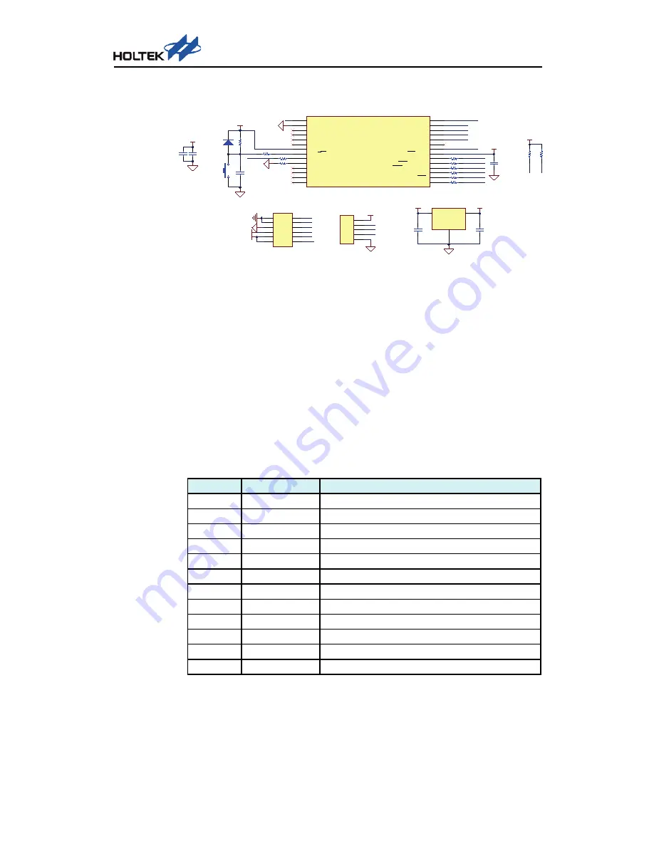
MCU Control Circuit
Figure 12 MCU Control Circuit
As the host MCU, the HT66F50 is mainly used to transfer data with the HT1635A/B via a
4-wire interface or an I
2
C interface and control the driver device to drive the RGB LED
Matrix for various display functions. In addition, the HT66F50 detects whether AC power
or an external power adapter is connected. It uses its A/D converter to sample the battery
voltage, controls the APL3202 to charge the battery or not and determines whether the
SY7066 is turned on for a battery voltage boost function. The HT66F50 has an integrated
12-bit SAR A/D converter, whose reference voltage is provided by the MCU operating
voltage being regulated to 2.5V using the HT7125. In the figure above, the pin header J5
is used for the HT1635A/HT1635B power and interface pins connection. J4 is used for the
HT66F50 In-Circuit programming pin connection.
HT66F50 I/O Control Functions:
MCU Pin
Circuit Label
Control Function
9
IO_CHG_DET
APL3202 charging status detection
15
KEY
Detects the key used for switching display functions
16
RDB
4-wire interface read serial clock
17
CSB1
4-wire interface HT1635A chip selection
18
CSB2
4-wire interface HT1635A chip selection
19
WRB
I
2
C/4-wire interface serial clock
20
DATA
I
2
C/4-wire interface serial data
22
IO_BOOSTEN
DC-DC boost enable control
24
IO_USBIN
External power adapter detection
25
IO_ACIN
AC power detection
26
AD_BAT1V
Li-battery voltage detection
28
IO_BAT1_CHGEN Li-battery charging enable control
VIN
2
VOUT
3
G
N
D
1
U2
HT7125-SOT89
ADC_VREF
0.1uF
C13
10uF
C14
MCU_VDD
100K
R21
0.1uF
C17
ADC_VREF
R
ES
ET
_K
EY
PA0/C0X/TP0_0/AN0
1
VSS/AVSS
2
PB4/XT2
3
PB3/XT1
4
PB2/OSC2
5
PB1/OSC1
6
VDD
7
PB0/RES
8
PC1/TP1B_1/SCOM1
9
PC0/TP1B_0/SCOM0
10
PC7/[TP1A]/SCOM3
11
PC6/[TP0_0]/SCOM2
12
PD3/[TCK1]/TP3_0/[SDO]
13
PD2/[TCK0]/[SDI/SDA]
14
PD1/[TP2_0]/[SDO]/[SCK/SCL]
15
PD0/[TCK2]/TP3_1/[SCS]
16
PC5/[INT1]/TP0_1/TP1B_2/[PCK]
17
PC4/[INT0]/[PINT]/TCK3/TP2_1
18
PC3/PINT/TP2_0/C1-
19
PC2/TCK2/PCK/C1+
20
PB5/SCS/VREF
21
PA7/SCK/SCL/AN7
22
PA6/SDI/SDA/AN6
23
PA5/C1X/SDO/AN5
24
PA4/INT1/TCK1/AN4
25
PA3/INT0/C0-/AN3
26
PA2/TCK0/C0+/AN2
27
PA1/TP1A/AN1
28
U5
HT66F50-28SOP-A
0.1uF
C15
MCU_VDD
0.1uF
C18
KEY
CSB1
RDB
WRB
DATA
CSB2
ICPDA
ICPCK
RST
AD_BAT1V
IO_ACIN
IO_BAT1_CHGEN
MCU_VDD
NC
C16
220R
R25
300R
R22
D8
1N4148
FB/471
R26
330R
R27
330R
R28
330R
R29
MCU_VDD
RST
ICPCK
ICPDA
1
2
3
4
5
J4
IO_BOOSTEN
NC
R31
NC
R32
MCU_VDD
W
R
B
D
A
TA
NC
R24
330R
R30
IO_CHG_DET
0R
R23
IO_USBIN
CSB1
RDB
WRB
DATA
CSB2
KEY
1
12
2
11
3
10
4
9
5
8
6
7
J5
GND1
VDD2
VDD1


