Rev. 1.50
14�
����st ��� �01�
Rev. 1.50
149
����st ��� �01�
HT66F0175/HT66F0185
A/D Flash MCU with EEPROM
HT66F0175/HT66F0185
A/D Flash MCU with EEPROM
LCD Frames
A cyclic LCD waveform includes two frames known as Frame 0 and Frame 1 for which the
following offers a functional explanation.
•
Frame 0
To select Frame 0, clear the FRAME bit in the SLCDC 0 register to 0.
In frame 0, the COM signal output can have a value of V
DD
or a V
BIAS
value of (1/3)×V
DD
. The SEG
signal output can have a value of V
SS
or a V
BIAS
value of (2/3)×V
DD
.
•
Frame 1
To select Frame 1, set the FRAME bit in the SLCDC0 register to 1.
In frame 1, the COM signal output can have a value of V
SS
or a V
BIAS
value of (2/3)×V
DD
. The SEG
signal output can have a value of V
DD
or a V
BIAS
value of (1/3)×V
DD
.
The COMn waveform is controlled by the application program using the FRAME bit in the
SLCDC0 register and the corresponding pin-shared I/O data bit for the respective COM pin to
determine whether the COMn output has a value of V
DD
, V
SS
or V
BIAS
. The SEGm waveform is
controlled in a similar way using the FRAME bit and the corresponding pin-shared I/O data bit for
the respective SEG pin to determine whether the SEGm output has a value of V
DD
, V
SS
or V
BIAS
.
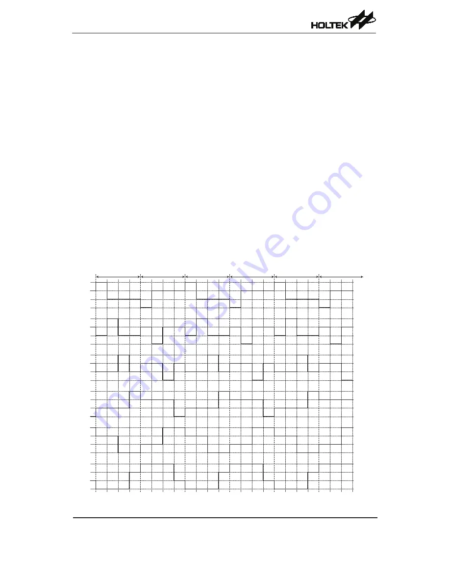
The accompanying waveform diagram shows a typical 1/3 bias LCD waveform generated using the
application program together with the LCD voltage select circuit. Note that the depiction of a “1”
in the diagram illustrates an illuminated LCD pixel. The COM signal polarity generated on pins
SCOM0~SCOM5, whether “0” or “1”, are generated using the corresponding pin-shared I/O data
register bit.
COM0
V
DD
(2/3) V
DD
(1/3) V
DD
V
SS
V
DD
(2/3) V
DD
(1/3) V
DD
V
SS
COM1
COM2
V
DD
(2/3) V
DD
(1/3) V
DD
V
SS
V
DD
(2/3) V
DD
(1/3) V
DD
V
SS
COM3
V
DD
(2/3) V
DD
(1/3) V
DD
V
SS
SEG0
V
DD
(2/3) V
DD
(1/3) V
DD
V
SS
SEG1
Frame 0
Frame 1
Frame 0
Frame 1
Frame 0
Frame 0
1
0
0
0
1
0
0
0
1
0
0
0
1
0
0
0
1
0
0
0
1
0
0
0
1
0
0
0
0
0
1
0
1
0
0
0
0
0
1
0
1
0
0
0
0
1
0
0
1
0
0
0
0
1
0
0
1
0
0
0
0
1
0
0
1
0
0
0
1
0
0
0
1
0
0
0
1
0
0
0
1
0
0
0
1
0
0
0
1
0
0
0
0
0
1
1
0
0
1
1
0
0
1
1
0
0
1
1
0
0
1
1
0
0
1
1
1
1
0
1
1
1
0
1
1
1
0
1
1
1
0
1
1
1
0
1
1
1
Note: The logical values shown in the above diagram are the corresponding pin-shared I/O data bit value.
1/3 Bias LCD Waveform – 4-COM & 2-SEG application


