Rev. 1.50
11�
����st ��� �01�
Rev. 1.50
119
����st ��� �01�
HT66F0175/HT66F0185
A/D Flash MCU with EEPROM
HT66F0175/HT66F0185
A/D Flash MCU with EEPROM
A/D Converter Register Description
Overall operation of the A/D converter is controlled using six registers. A read only register pair
exists to store the A/D Converter data 12-bit value. One register, ACERL, is used to configure the
external analog input pin function. The remaining three registers are control registers which setup
the operating and control function of the A/D converter.
Register
Name
Bit
7
6
5
4
3
2
1
0
S�DOL
(�DRFS=0)
D3
D�
D1
D0
—
—
—
—
S�DOL
(�DRFS=1)
D�
D6
D5
D4
D3
D�
D1
D0
S�DOH
(�DRFS=0)
D11
D10
D9
D�
D�
D6
D5
D4
S�DOH
(�DRFS=1)
—
—
—
—
D11
D10
D9
D�
S�DC0
ST�RT
�DBZ
�DCEN
�DRFS
—
S�CS� S�CS1 S�CS0
S�DC1
S�INS�
S�INS10 S�INS0
—
—
S�CKS� S�CKS1 S�CKS0
S�DC�
�DPG�EN VBGEN VREFIPS VREFPS S�VRS3 S�VRS� S�VRS1 S�VRS0
�CERL
�CE�
�CE6
�CE5
�CE4
�CE3
�CE�
�CE1
�CE0
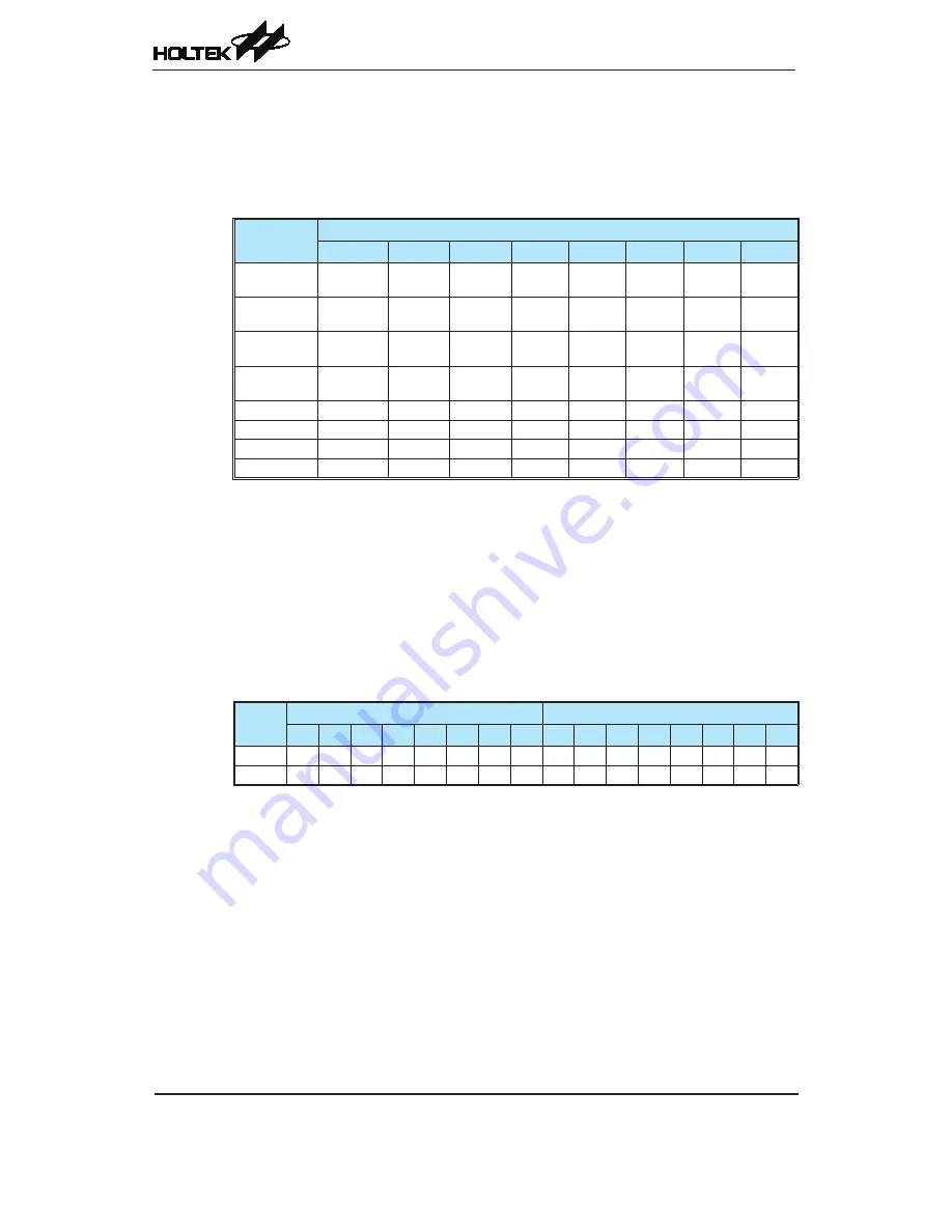
A/D Converter Registers List
A/D Converter Data Registers – SADOL, SADOH
As these devices contain an internal 12-bit A/D converter, it requires two data registers to store the
converted value. These are a high byte register, known as SADOH, and a low byte register, known
as SADOL. After the conversion process takes place, these registers can be directly read by the
microcontroller to obtain the digitised conversion value. As only 12 bits of the 16-bit register space
is utilised, the format in which the data is stored is controlled by the ADRFS bit in the SADC0
register as shown in the accompanying table. D0~D11 are the A/D conversion result data bits. Any
unused bits will be read as zero. The A/D data registers contents will keep unchanged if the A/D
converter is disabled.
ADRFS
SADOH
SADOL
7
6
5
4
3
2
1
0
7
6
5
4
3
2
1
0
0
D11 D10 D9 D� D� D6 D5 D4 D3 D� D1 D0
0
0
0
0
1
0
0
0
0
D11 D10 D9 D� D� D6 D5 D4 D3 D� D1 D0
A/D Converter Data Registers


