Rev. 2.10
118
���� 02� 201�
Rev. 2.10
119
���� 02� 201�
HT68F20/HT68F30/HT68F40/HT68F50/HT68F60
HT68FU30/HT68FU40/HT68FU50/HT68FU60
Enhanced I/O Flash Type 8-Bit MCU with EEPROM
HT68F20/HT68F30/HT68F40/HT68F50/HT68F60
HT68FU30/HT68FU40/HT68FU50/HT68FU60
Enhanced I/O Flash Type 8-Bit MCU with EEPROM
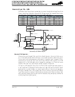
PWM Output Mode
To select this mode, bits TnM1 and TnM0 in the TMnC1 register should be set to 10 respectively.
The PWM function within the TM is useful for applications which require functions such as motor
control, heating control, illumination control etc. By providing a signal of fixed frequency but
of varying duty cycle on the TM output pin, a square wave AC waveform can be generated with
varying equivalent DC RMS values.
As both the period and duty cycle of the PWM waveform can be controlled, the choice of generated
waveform is extremely flexible. In the PWM mode, the TnCCLR bit has no effect on the PWM
operation. Both of the CCRA and CCRP registers are used to generate the PWM waveform, one
register is used to clear the internal counter and thus control the PWM waveform frequency, while
the other one is used to control the duty cycle. Which register is used to control either frequency
or duty cycle is determined using the TnDPX bit in the TMnC1 register. The PWM waveform
frequency and duty cycle can therefore be controlled by the values in the CCRA and CCRP registers.
An interrupt flag, one for each of the CCRA and CCRP, will be generated when a compare match
occurs from either Comparator A or Comparator P. The TnOC bit in the TMnC1 register is used to
select the required polarity of the PWM waveform while the two TnIO1 and TnIO0 bits are used to
enable the PWM output or to force the TM output pin to a fixed high or low level. The TnPOL bit is
used to reverse the polarity of the PWM output waveform.
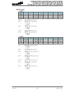
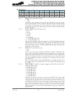
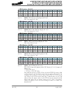
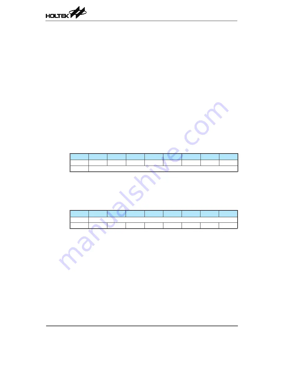
CTM, PWM Mode, Edge-aligned Mode, TnDPX=0
CCRP
001b
010b
011b
100b
101b
110b
111b
000b
Period
128
256
38�
512
6�0
768
896
102�
D�t�
CCRA
If f
SYS
=16MHz, TM clock source is f
SYS
/4, CCRP=100b and CCRA=128,
The CTM PWM output frequency=(f
SYS
/4)/512=f
SYS
/2048=7.8125kHz, duty=128/512=25%.
If the Duty value defined by the CCRA register is equal to or greater than the Period value, then the
PWM output duty is 100%.
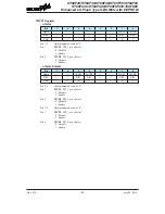
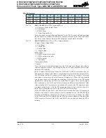
CTM, PWM Mode, Edge-aligned Mode, TnDPX=1
CCRP
001b
010b
011b
100b
101b
110b
111b
000b
Period
CCRA
D�t�
128
256
38�
512
6�0
768
896
102�
The PWM output period is determined by the CCRAregister value together with the TM clock while
the PWM duty cycle is defined by the CCRP register value.


