Rev. 2.10
32
���� 02� 201�
Rev. 2.10
33
���� 02� 201�
HT68F20/HT68F30/HT68F40/HT68F50/HT68F60
HT68FU30/HT68FU40/HT68FU50/HT68FU60
Enhanced I/O Flash Type 8-Bit MCU with EEPROM
HT68F20/HT68F30/HT68F40/HT68F50/HT68F60
HT68FU30/HT68FU40/HT68FU50/HT68FU60
Enhanced I/O Flash Type 8-Bit MCU with EEPROM
RAM Data Memory
The Data Memory is a volatile area of 8-bit wide RAM internal memory and is the location where
temporary information is stored.
Structure
Divided into two sections, the first of these is an area of RAM, known as the Special Function Data
Memory. Here are located registers which are necessary for correct operation of the device. Many
of these registers can be read from and written to directly under program control, however, some
remain protected from user manipulation.
The second area of Data Memory is known as the General Purpose Data Memory, which is reserved
for general purpose use. All locations within this area are read and write accessible under program
control.
The overall Data Memory is subdivided into several banks, the structure of which depends upon
the device chosen. The Special Purpose Data Memory registers are accessible in all banks, with
the exception of the EEC register at address 40H, which is only accessible in Bank 1. Switching
between the different Data Memory banks is achieved by setting the Bank Pointer to the correct
value. The start address of the Data Memory for all devices is the address 00H.
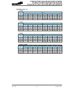
Device
Capacity
Bank
HT68F20
6�×8
0: 60H~7FH
1: 60H~7FH
HT68F30
96×8
0: 60H~7FH
1: 60H~7FH
2: 60H~7FH
HT68F�0
192×8
0: 80H~FFH
1: 80H~BFH
HT68F50
38�×8
0: 80H~FFH
1: 80H~FFH
2: 80H~FFH
HT68F60
576×8
0: 80H~FFH
1: 80H~FFH
2: 80H~FFH
3: 80H~FFH
�: 80H~BFH

