SYSTEM DESCRIPTION AND INSTALLATION MANUAL
HS--700 High Speed Data System
23--20--33
30 Aug 2002
Use or disclosure of information on this page is subject to the restrictions in the proprietary notice of this document.
Page 3--10
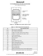
Figure 3-9. HSU CDM Connector (X3) Pin Layout
Table 3-3. HSU X3 Connector Pin Assignments
Pin
Signal Name/Description
1
CS -- Chip Select Signal to the CDM (Active Low)
2
SO -- Serial Output Data from the CDM
3
WP -- Write Protect Signal to the CDM (Active Low)
4
NC -- Not Connected
5
SI -- Serial Input Data to the CDM
6
SCK -- Serial Clock to the CDM (2 MHz maximum)
7
ADR0 -- Address output to the CDM (5 V/10 mA maximum)
8
ADR1/ ID Input -- Output: 3 V Levels (Tri--state), Input: 3 V or 5 V Levels and
10 Kohm pull down resistor
9
VCC -- Power Supply Voltage to the CDM (3.3 V
±
0.15 V, 5 mA maximum)
Shield
GND -- Sheild must be connected internally to ground
B. CDM
(1) The CDM is connected to the X1 connector of the HSU. Refer to paragraph 3.A.(4) in
this section for electrical installation information for the HSU X1 connector.


