background image

Summary of Contents for 202A

Page 1: ... ve added this manual to the Agilent website in an effort to help you support your product This manual provides the best information we could find It may be incomplete or contain dated information and the scan quality may not be ideal If we find a better copy in the future we will add it to the Agilent website Support for Your Product Agilent no longer sells or supports this product You will find ...

Page 2: ......

Page 3: ......

Page 4: ......

Page 5: ...on all ranges except X100 Less than 2 rms on X100 OUTPUT SYSTEM Can be operated either balanced o r single ended Output system is direct coupled dc level of output voltage remains stable over long periods of time DC adjustment available on front panel HUM LEVEL Less than 0 05 at rated output SYNC PULSE 10 volts peak negative less than 5 microseconds duration Sync pulse occurs at crest of sinewave ...

Page 6: ...ut System III 3 6 Sync Pulse Output III 3 7 Powersupply III SECTION IV MAINTENANCE General I V 1 Power Supply IV 1 Function Generator bi stable circuit and integrator IV 2 Sine Synthesizer and Function Selector IV 2 Output Amplifier IV 3 sync Out IV 3 Tube Replacement IV 3 Tube Replacement Chart IV 4 Power Supply Regulator Adjustment N 4 Theory of DC Balance and Distortion Adjustments IV 5 DC Bala...

Page 7: ...the triangular wave Output amplitude and distortion are virtually in dependent of the frequency of operation This type SECTION I GENERAL DESCRIPTION of oscillating system in inherent a constant am plitude device so that no A V C system with as sociated delay in stabilization after frequency changes is required The frequency range from 008 to 1200 cycles per second is covered in 5 bands The frequen...

Page 8: ......

Page 9: ...RATING INSTRUCTIONS OUTPUT This group consists of three terminals The one marked G is connected directly to the instrument chassis The other two terminals vertically aligned are the OUTPUT terminals With respect to the ground terminal each of these outputs has equal magnitude of signal but they are 180 out of phase with each other The internal impedance between the two OUTPUT terminals is appmxima...

Page 10: ...stive will shunt the impedance existing between the two signal inputs of the system being driven Under circumstances where the connection places the Model 202A in series with a path carrying cur rent distortion of the Model 202A output will occur if greater than 10 ma peak current is caused to flow through the Model 202A output system NOTES When small output voltages are required it may be To mini...

Page 11: ...he bi stable circuit THEORY OF OPERATION is that seen between points B and D The conversion of square wave to triangular wave takes place in the integrator unit which is carefully designed to produce an accurate integral of the applied square wave The bi stable circuit and linear integrator are loop coupled in such a manner that the resulting relaxation oscillator is suitable for very low fre quen...

Page 12: ...e bi stable circuit Actually this circuit is a combination of two circuits If capa citors C10 and C13 are disconnected so that there is no possibility of inductive coupling from grids to cathode of V1 and V2 the remaining circuit is the well known flip flop or Eccles Jordan trigger circuit The other circuit which appears in the bi stable circuit is a voltage comparator known as the Multiar The mul...

Page 13: ...l at the junction of R and C the output voltage must also be triangular In this case the frequency of the applied signal is so low that the amplifier used must be direct coupled There is a net voltage rise between input level and output level in a dc amplifier In this particular application the average output level is determined a s the average of the plus reference and minus reference levels sinc...

Page 14: ...wer is used a s an isolation stage between the integrator and the bi stable circuit This completes the oscillating loop with its inherent production of both square and triangular functions 3 4 SINE SYNTHESIZER A N D FUNCTION SELECTO R SWITCH The triangular wave from the linear integrator is connected to R94 In the SINE position of the FUNC TION selector switch 53 the other end of R94 is connected ...

Page 15: ...Triangular regardless of function selector position w B Waveform from to B with selector switch in sine position Note distortion especially at peaks C Waveform from to B with selector switch in sine position This is the distortion component present in waveform B above D Waveform fromato i e difference between waveforms B and C above This is the approxi mated sinewave RO Figure 3 6 50 IL Waveforms ...

Page 16: ...placed by R95 so that the combination R94 and R95 is a simple linear divider for all voltage levels It is adjusted to give equal sine and triangular wave peak magnitude The squarewave is connected to the FUNCTION selector switch through the divider R59 and R22 which adjusts the average voltage of the squarewave to the voltage at the cathode of V4 In the squarewave position of the selector switch R...

Page 17: ...e level for operation has been B and in the Model 202A the B line is completely isolated from the chassis Thus the chassis ground is available for whatever connection is desired It is possible to consider the two output terminals a s a transformer output and further to balance this apparent transformer to chassis by making R98 equal to R99 The capacitor C29 insulates the apparent transformer secon...

Page 18: ... primary The resistor and diode in the secondary remove the positive excursion resulting in a negative pulse at the SYNC OUT ter minals 3 7 POWER SUPPLY The Power Supply is a full wave rectifier and regula tor which supplies 375 volts The 75 volt and 225 volt regulated outputs are taken from a voltagc divider across the 375 volt supply The main requirement on the three regulated voltages is very l...

Page 19: ...eter o r oscilloscope to eliminate the dc component Interaction between most of the circuits of the Model 202A makes a fairly definite procedure for trouble shooting necessary For example a fault in the oscillator section may easily cause considerable voltage deviations in the output system Therefore it is more desirable to divide the instrument into five sections a s follows and consider each in ...

Page 20: ...ed and the necessary adjustments made an oscilloscope should be connected between pin 3 tube V17 and B to see if a good triangular waveform is obtained on all ranges TABLE 4 2 1 Sine Wave Observe the waveform between pin 2 V18 and B with oscillator set to 50 cycles sec and the AMPLITUDE control a t maximum Set the FUNCTION switch in the SINE position The wave form should be substantially sinusoida...

Page 21: ...nal chassis and main chassis See para graph 4 9 See paragraph 4 4 Replace variable resistor R93A R93B Adjust regulated voltage See para graph 4 9 Replace Vl8 Vl9 v20 Excessive humfrom power supply See paragraph 4 9 The distortion should remain within specifi cations when the output is loaded with 4000 ohms or higher The peak to peak output voltage should be at least 30 volts 10 6 volts rms with a ...

Page 22: ...rtion o r dc balance from change in regulated voltages Same effect a s change in V3 possible but to much less degree Frequency change and unbalance of triangle Change in dc output component independent of AMPLITUDE control setting No effect Possible change in 375 and 225 regulated voltages 2 Connect the 202A to the power line and turn on The voltmeter indication should be between 190 and 230 volts...

Page 23: ...ies the dc level of the signal on one grid of the second stage of the amplifier When these adjustments are made the dc component between the output terminals will remain at a very low value independent of amplitude setting or waveform selected Control R49 varies the level to which the output of the integrator rises in a positive direction and A51 varies the level of the negative excursion The b 6 ...

Page 24: ...in the output sine wave at 100 cps first on the X10 RANGE with the FRE QUENCY dial at 10 then on the XlOO RANGE with the FREQUENCY dial at 1 I the distortion indi cations are not approximately identical careful adjustment of R119 will lower the 100cps distortion on the XlOO RANGE 18 Connect the voltmeter COMMON lead to the common junction of AMPLITUDE controls R93A and R93B violet wire Connect the...

Page 25: ...en by peak flattening on one side and sharpening on other Also sine average not same as triangle D References are correct but tri angle unbalanced Frequency correct but high second harmonic component in phase with funda Triangle Sine Ave mental Figure 4 2 Effect of Triangle Maladjustment on Distortion and Frequency Ten Segment Approximations Used for Clarity ...

Page 26: ... of the X1 range The out put frequency should be within 2 of the dial reading over the entire range Adjust by substituting different resistor values for R26 The location of R26 is shown in Figure 4 3 5 Determine the ratio between the two frequencies obtained with the frequency dial at 0 8 and 12 with the RANGE switch at Xl Frequency determination is most easily accomplished by measuring the period...

Page 27: ...and The maximum value for this capacitor is 300 ppf and any value less than this may be used This capacitor is not required in all instruments and is not shown on the schematic diagram 10 Replace the cabinet or the top and bottom cover 4 14 REPLACEMENT O F R 5 8 POTENTIOMETER Replacement of the frequency control potentiometer involves two basic operations 1 The mechanical procedure for replacing a...

Page 28: ...COUPLER ACCESS Figure 4 4 Model 202A Top View Cover Removed ...

Page 29: ...Figure 4 5 Model 202A Bottom View Bottom Plate Removed ...

Page 30: ...Figure 4 6 Model 202A Function Generator and Amplifier ...

Page 31: ...ER OF l22MEGOHMS INPUT RESISTANCE rf7 INTERNAL CHASSIS ONE POINT CONNECTION TO DIVIDER 0 I S ANY BLACK LEAD IN POWER SUPPLY EXCEPT T I R78 8 R79 PRIMARY START POWER SUPPLY RETURN I S NOT CONNECTED TO CHASSIS PRI 2 3 PANEL CONTROLS SET AS FOLLOWS BLACK TI PRI I BROWN PRI 2 RANGE AT XIO FREQUENCY AT 5 FUNCTION AT SINE AMPLITUDE AT MAX CAPACITY I N L VF UNLESS OTHERWISE NOTED 2024 P S 5 3 1 1 A ELECT...

Page 32: ...be l i s t e d on a Production Change s h e e t at the front of t h i s manual When o r d e r i n g p a r t s f r o m t h e f a c t o r y a l w a y s i n c l u d e t h e f o l l o w i n g i n f o r m a t i o n I n s t r u m e n t M o d e l N u m b e r S e r i a l N u m b e r S t o c k N u m b e r of P a r t D e s c r i p t i o n of P a r t ...

Page 33: ...Sect V Page 2 TABLE O F REPLACEABLE PARTS Total quantity used in the instrument ...

Page 34: ...Sect V Page 3 T A B L E O F REPLACEABLE PARTS Total quantity used in the instrument ...

Page 35: ...Sect V Page 4 T A B L E OF REPLACEABLE PARTS Total quantity used in the instrument ...

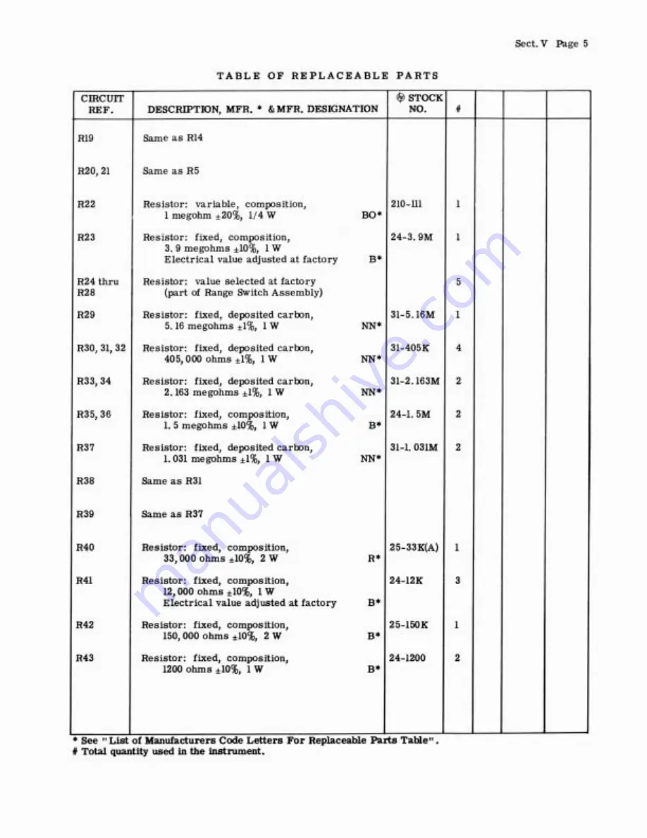
Page 36: ...Sect V Page 5 T A B L E O F REPLACEABLE PARTS ...

Page 37: ...Sect V Page 6 T A B L E O F REPLACEABLE PARTS Total quantity used in the instrument ...

Page 38: ...Sect V Page 7 T A B L E O F REPLACEABLE PARTS ...

Page 39: ...d 2500 ohms lo 10 W S Same a s R62 Resistor variable composition 2 sections 1megohmlsect 20 114W BO Same a s R53 Resistor fixed deposited carbon 67 500 ohms l 112 W NN Same a s R6 Resistor fixed deposited carbon 15 800 ohms 1 1W NN These circuit references not assigned R103 R104 105 R106 R107 R108 See List Total quantity Resistor fixed composition 4 1800 I 1800 ohms lo 1W B Resistor fixed wirewoun...

Page 40: ...gohms lo 112 W Resistor variable composition 500 000 ohms linear taper Resistor variable wirewound 500 ohms 2 W linear NN NN NN NN NN NN B G BO 1s1 I Switch toggle SPST D 310 11 I Range Switch Assembly includes R24 1s2 1 thru R29 ClS thru C18 HP I202A 19W Function Switch Assembly includes 202A 19B R94 R95 HP Transformer power Transformer pulse Transformer pulse Tube electron 6AU6 Paeco 910 79 Paec...

Page 41: ...Sect V Page 10 T A B L E O F REPLACEABLE PARTS ...

Page 42: ...Sect V Page 1 1 T A B L E O F R E P L A C E A B L E P A R T S Total quantity used in the instrument ...

Page 43: ...ladelphia 24 Pa Philadelphia 44 Pa West Orange N J North Chicago Ill Keasbey N J Sunnyvale Calif CODE LETTER MANUFACTURER Hammerlund Mfg Co Inc Industrial Condenser Corp lnsuline Corp of America Jennings Radio Mfg Corp E F Johnson Co Lenz Electric Mfg Co Micro Switch Mechanical Industries Prod Co Model Eng Mfg Inc The Muter Co Ohmite Mfg Co Resistance Products Co Radio Condenser Co Shallcross Manu...

Page 44: ...instrument is returned transportation charges prepaid by the original purchaser and when upon our examination it is disclosed to our satisfaction to be defective If the fault has been caused by misuse or abnormal conditions of operation repairs will be billed at cost In this case an estimate will be submitted before the work is started If any fault develops the following steps should be taken 1 No...

Page 45: ...able ceramic 7 45uuf9 500 vdcw hp Stock NO 13 1 Mfr L R24 thru Delete R28 R24A 25A9 Add r e s i s t o r fixed deposited carbon 900 000 ohms 26A927A m 1 W hp Stock NO 31 900K Mfr NN E l e c t r i c a l value adjusted a t the factory R28A Add r e s i s t o r fixed deposited carbon 800 000 ohms m91 W hp Stock Noo 31 800K Mfr NN E l e c t r i c a l value ad justed a t the factoryo R24B925B9 Add r e s ...

Page 46: ... X ltl range R27B for the X10 range and R28B for the X100 range On the X100 range only adjust C33 to calibrate the high end of the band Serial 6800 and above also Serials 6411 6747 6750 6751 67529 67539 67549 67559 6756 67579 6758 C1 2 Change to capacitor fixed electrolytic 20uf 450 vdcw hp Stock No 18 20HP Mfr CC Add capacitor fixed electrolytic 2 sections 20uf sect 450 vdcw hp Stock No 18 22HP M...

Page 47: ......

Reviews: