Section IV
Model 3300A
4-10.
The sync pulse is produced by an RC
differentiating network. The negative pulse at the output
is in phase with the positive crest of the sine and triangle
wave.
4-11.
Power Supply (Refer to Figure 6-5) can operate
on either 115 or 230 volts input and delivers 3 pairs of
voltages, +40V, ±26.5V, and +20V. The 40 volt supply
provides power for the oven heater. The 26.5 volt
supplies are regulated and the 20 volt supplies are double
regulated.
4-12.
Critical temperature sensitive components are
housed within an oven in which the temperature is
maintained at approximately 800 C (1760 F).
4-13.
SCHEMATIC THEORY.
4-14.
FREQUENCY CONTROL NETWORK.
4-15.
(Refer to Figure 6-2) The FREQUENCY dial (R4)
in conjunction with the RANGE switch (S3) provides
internal frequency control. The basic frequency equation
can be expressed as F= i
2C
∆
e out
where i is the current to the triangle integrator, C is the
triangle integrator feedback capacitor and e out is the
peak-to-peak voltage of the triangle wave.
4-16.
The position of the RANGE switch determines the
integrating capacitor C. The FREQUENCY dial or
external control voltage determines the current i. The
frequency control voltage is applied to the current control
transistor Al IQ5, which establishes the amount of current
available to the triangle integrator from the current
sources AllQ6 and AllQ7.
4-17.
CURRENT SOURCES.
4-18.
The state of current source A11Q6 is controlled
by the voltage comparator multivibrator, and in turn,
controls the direction of the current in the input of the
triangle integrator. When A11Q6 is on, a current, 2 i,
flows through it and divides, i into the integrator and i
through current source A11Q7. When the bi-stable
multivibrator changes state and gates A11Q6 off, 2 i no
longer flows; however, the current through A11Q7
remains the same. Therefore, a current equal to i but
opposite in direction flows from the triangle integrator
input.
4-19.
TRIANGLE INTEGRATOR.
4-20.
The triangle integrator consists of an impedance
converter A11Q8 (a field effect transistor), a differential
amplifier A13Q1 and A13Q2, an emitter follower A13Q3,
diode A13CR1, and the capacitive feedback network: this
circuit integrates the constant current inputs into the
positive and negative slopes which make up the triangle
wave. The triangle wave is applied to the inputs of the
output amplifiers, sine wave synthesizer and voltage
comparator multivibrator.
4-21.
VOLTAGE COMPARATOR MULTIVIBRATOR.
4-22.
The voltage comparator multivibrator consists of
a voltage comparator switching network, A14Q8,
A14CR13 and A14CR14; a bi-stable multivibrator A14Q9
and Q10 and an emitter follower A14Q11. A14CR19 and
R45 provide a low resistive path to ensure rapid rise and
fall time of the square wave in the event the capacitance
of the load is high. When the positive slope of the triangle
wave r20 volts, A14CR13 is turned on. A14Q9
is then turned on which turns A14Q10 off. The rise in the
collector voltage of A14Q10 is coupled through emitter
follower A14Q11 and through A14CR20 and A14CR21
into the emitter circuit of A11Q6, and turns it on. The
output slope then becomes negative. A11Q6 remains on
until the negative slope reaches zero volts. At the zero
point on the negative slope A14CR14 is turned on which
causes the bi-stable multivibrator to change state so that
A14Q9 is now off and A14Q10 is on. The decrease in
A14Q10 collector voltage gates the current source,
A11Q6, off which reverses the integrator input current.
The positive slope then begins increasing toward the
upper limit, +20 volts. The output of the emitter follower is
differentiated by A14C7 and A14R48 to provide the sync
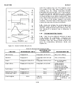
output. A negative sync pulse occurs at the crest of sine
and triangular wave, see Figure 4-1.
4-23.
SINE WAVE SYNTHESIZER.
4-24.
(See Figure 6-2) The sine wave synthesizer
comprises four control transistors, the biased diodes with
associated voltage dividers, a differential amplifier
A14Q5, A14Q6 and the output amplifier A14Q7. A14R17
andA14R29 adjust the operating points of the voltage
dividers to minimize distortion. The diodes are biased by
the four control transistors A14Q1 through A14Q4 and the
voltage dividers to provide twelve different current paths
in the input to the differential amplifier as the triangle
wave progresses. Each slope of the triangle wave is
modified in twelve steps so that the waveform appearing
at the base of A14Q5 approximates a sine wave. The
sine wave synthesizing network is isolated by the
differential amplifier A14Q5 and A14Q6 and amplifier
A14Q7.
4-25.
OUTPUT AMPLIFIERS. Figure 6-4).
4-26.
The etched circuit assemblies A15 and A16 are
identical. CHANNEL A and CHANNEL B differ due to the
-A output of CHANNEL B. The input for CHANNEL B with
its function switch in -A position, A16 Pin 5, is taken from
the junction of A15R20 and R21, XA15 Pin 11. The
output amplifiers are variable gain amplifiers. Gain is
varied by changing the amount of feedback for the
different functions. The following reference designators
should be prefixed by applicable assembly number. The
feedback is varied by resistors R1 through R5 and R23
C8 combination, to maintain equal peak-to-peak
amplitude of the various functions for a given
AMPLITUDE control setting. A differential amplifier, Q1
and Q2, make up the first stage followed by two additional
amplifiers Q3 and Q4. The trimmer C2 in the feedback
network is used to shape the square wave. The
AMPLITUDE control provides a nominal 600 ohms output
impedance, independent of amplitude control setting.
4-2
Summary of Contents for 3300A
Page 31: ...Model 3300A Section VI Figure 6 1 3300A Top and Bottom Views 6 2 ...
Page 32: ...Model 3300A Section VI Figure 6 2 Oscillator Circuit Schematic A11 A13 and A14 6 3 ...
Page 33: ...Model 3300A Section VI Figure 6 4 Output Amplifiers Schematic A15 and A16 6 5 6 6 ...
Page 34: ...TM 11 6625 2495 14 P THIS PAGE CURRENTLY NOT AVAILABLE FOR DIGITIZATION PAGE Figure 6 3 6 4 ...
Page 35: ...Model 3300A Section VI Figure 6 5 Power Supply Schematic A12 and A11 6 7 6 8 ...
Page 36: ...Model 3300A Section VI Figure 6 6 J6 Plug In Receptacle 6 9 ...
Page 58: ...SECTION IV REMARKS REFERENCE REMARKS CODE A Visuals B Performance checks D 5 ...
Page 60: ......
Page 61: ...PIN 046175 000 ...


