TM 11-6625-3071-14
3478A
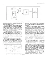
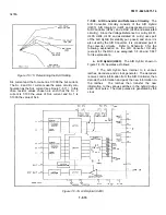
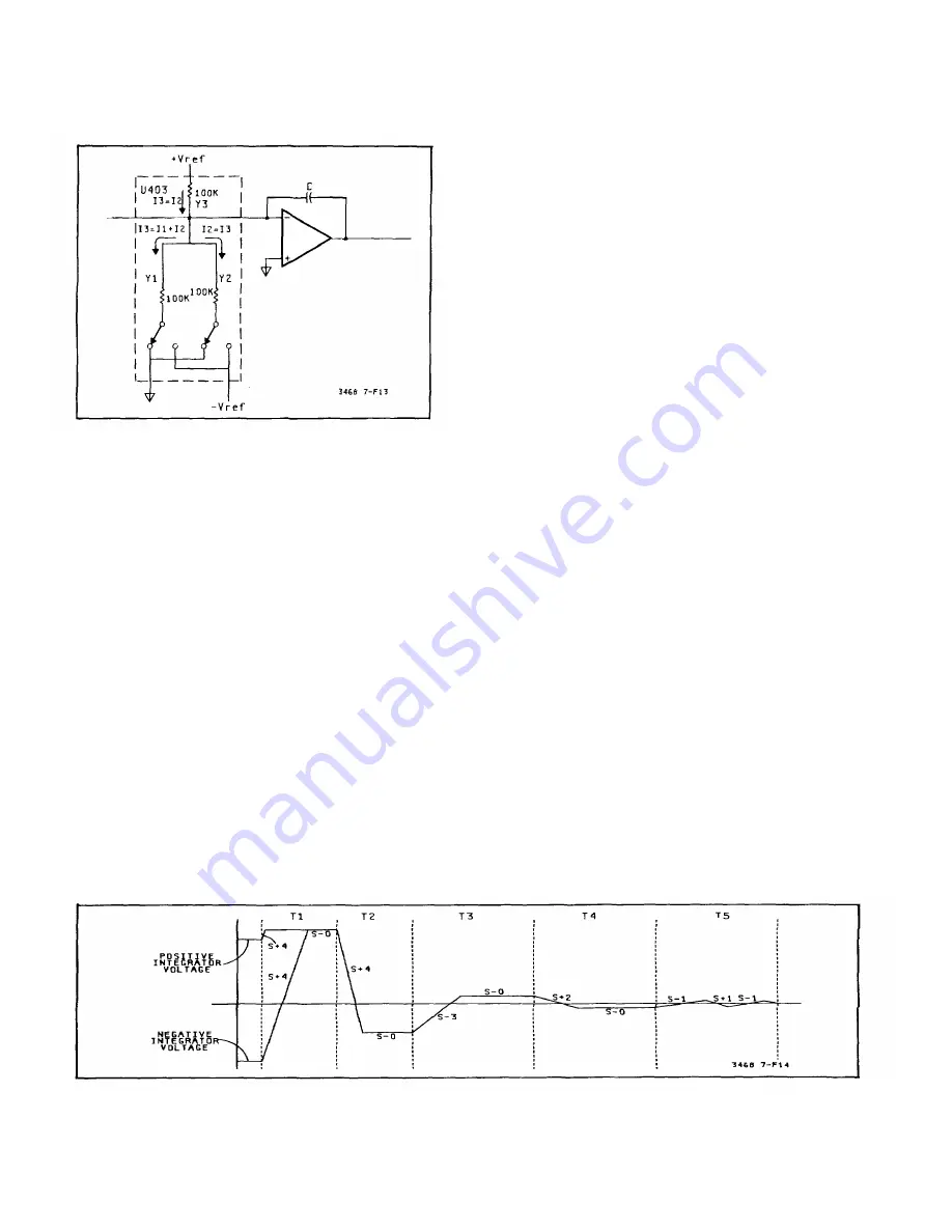
Figure 7-F-13. Slope S+0 and S-0 Generation
ference is that paths Y1 and Y2 are switched when the
slopes are switched (YI to ground and Y2 to -Vref, or Y2
to ground and Y1 to -Vref).
7-F-40. Runup Time. The runup time changes with the
number of digits selected. For the 3 1/2 Digit mode, the
time is 1/600 second (for both the 60Hz and the 50Hz
options) and is called .1 PLC (Power Line Cycles). For
the 4 1/2 Digit mode, the time is 1/60 second (1/50
second for the 50 Hz option) and is called 1 PLC. The 5
1/2 Digit mode is different. In this mode, 1 PLC is used
for the runup time with the A/D operation repeated ten
times. The resultant ten readings are then averaged and
the answer becomes a single reading.
7-F-41. Digit Generation. When the 3478A is in the 4
1/2 and 5 1/2 Digit mode, the first two significant digits
(of the reading) are determined during runup. In the 3 ½
Digit mode, only the first digit is determined. In run-
down, the three least significant digits are determined in
all modes. A total of 5 /2 digits are developed in both the
51/2 and 4/2 digit modes. Since only 412 digits are
displayed in the 41/2 digit mode, the last digit in the
mode is rounded off to the next higher digit.
7-F-42. Rundown. When runup is completed, the
voltage at the A/D Converter's input is removed and the
input is then connected to ground. The rundown opera-
tion then starts. Rundown is used to determine the three
least significant digits of the 3478A's reading.
7-F-43. After runup, a voltage (or charge) remains on
the integrator with its amplitude and polarity dependent
on the last current applied (S + 4 or S-4) and the input
voltage (applied during runup). By obtaining the value of
the remaining voltage, the least significant digits can then
be determined. The voltage value is obtained by
applying various currents to the integrator and counting
the number of of times the currents have to be applied
for the resultant output slopes of the integrator to cross
zero.
7-F-44. The currents applied to the integrator are called
the S-4, S + 4, S-3, S + 2, S-1, and S + 1 currents and
the resultant output slopes are the S-4, S + 4, S-3, S + 2,
S-1, and S + 1 slopes. Each one of the currents (S4, S +
4, etc.) are applied (in the given order) to the integrator a
set number of times until zero crossing occurs. The only
exception is the first S4 current (see paragraph 7-F-45
step c). The first and second set of currents applied are
the S-4 and S + 4 currents, respectively. These currents
have the same value as the S-4 and S + 4 currents used
in the runup operation, but are applied half as long. The
S-4 and S + 4 slopes are each 15 ALE cycles long (30
ALE cycles in runup) and are called half-ramps. The
next currents applied (in order) are the S-3, S + 2, and S-
1 currents, with S- slopes applied between them.
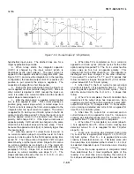
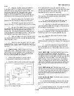
7-F-45. Rundown time is separated into five time
periods, as shown in Figure 7-F-14. Refer to the figure
for the following explanation on the rundown opera- tion.
a.
When rundown starts, the polarity of the
remaining voltage on the integrator is determined by the
A/D Controller (U462). The polarity is determined by the
output state of the A/D comparator (CMP output at U403
pin 11). A high output level shows a positive voltage and
a low level shows a negative voltage.
Figure 7-F-14. Rundown Slopes
7-F-13
Summary of Contents for 3478A
Page 2: ...TM 11 6625 3071 14 A ...
Page 4: ...TM 11 6625 3071 14 C D BLANK ...
Page 12: ...TM 11 6625 3071 14 Table 1 1 Specification 1 2 ...
Page 13: ...TM 11 6625 3071 14 Table 1 1 Specifications Cont 1 3 ...
Page 14: ...TM 11 6625 3071 14 Table 1 1 Specifications Cont 1 4 ...
Page 53: ...TM 11 6625 3071 14 1 ...
Page 54: ...TM 11 6625 3071 14 2 ...
Page 55: ...TM 11 6625 3071 14 3 ...
Page 56: ...TM 11 6625 3071 14 4 ...
Page 87: ...TM 11 6625 3071 14 3478A Figure 7 D 3 Flowchart B 7 D 5 ...
Page 88: ...TM 11 6625 3071 14 3478A Figure 7 D 4 Flowchart C 7 D 6 ...
Page 91: ...TM 11 6625 3071 14 3478A Figure 7 D 6 Flowchart D 7 D 9 ...
Page 111: ...TM 11 6625 3071 14 Figure 7 F 17 3478A Simplified Reference Circuitry 7 F 16 ...
Page 122: ...TM 11 6625 3071 14 Table A 2 A 2 HP IB Worksheet A 4 ...
Page 137: ...TM 11 6625 3071 14 Figure 7 D 2 Flow chart A 7 D 3 ...
Page 139: ...TM 11 6625 3071 14 Figure 7 G 2 3478A Block Diagram 7 G 3 ...
Page 140: ...TM 11 6625 3071 14 Component Locator for Input Circuitry and Ohms Current Source 7 G 4 ...
Page 141: ...TM 11 6625 3071 14 Figure 7 G 3 Input Circuitry and Ohms Current Source 7 G 5 ...
Page 142: ...TM 11 6625 3071 14 F G 6 ...
Page 143: ...TM 11 6625 3071 14 2 Figure 7 G 4 AC to DC Converter 7 G 7 ...
Page 144: ...TM 11 6625 3071 14 Component Locator for A D Converter and Control Logic 7 G 8 ...
Page 145: ...TM 11 6625 3071 14 3 Figure 7 G 5 A D Converter and Control Logic 7 G 9 ...
Page 146: ...TM 11 6625 3071 14 7 G 10 ...
Page 147: ...TM 11 6625 3071 14 4 Figure 7 G 6 Power Supplies 7 G 11 7 G 12 blank ...
Page 148: ......
Page 149: ...PIN NO 057444 ...

