TM 11-6625-3071-14
3478A
cuitry and Floating Common Logic Circuitry.
Communications between the circuitry is done by the
Isolation Logic. The circuitry is described as follows:
4-F-52. Chassis Common Circuitry - paragraph 7-F-
55.
a.
Main CPU (USO1) Circuitry - paragraph 7-F-57.
b.
Control ROM (U502) - paragraph 7-F-58.
c.
Power-On and Reset Circuitry - paragraph 7-F-
59.
d.
CMOS RAM - paragraph 7-F-60.
e.
RAM Addressing - paragraph 7-F-61.
f.
Reading the RAM - paragraph 7-F-62.
g.
Sending Data to the RAM paragraph - 7-F-63.
h.
Keyboard Operation - paragraph 7-F-65.
i.
Display Operation - paragraph 7-F-66.
j.
HP-IB Operation - paragraph 7-F-67.
k.
Rear Panel Switch Circuitry - paragraph 7-F-68.
I.
Voltmeter Complete - paragraph 7-F-69.
m. External Tigger - paragraph 7-F-70.
7-F-53. Isolation Logic - paragraph 7-F-71.
7-F-54. Floating Common Logic Circuitry - paragraph
7-F-75.
a.
A/D Controller (U462) Operation-paragraph 7-F-
77.
b.
A/D Converter Control - paragraph 7-F-78.
c.
Input Hybrid Control - paragraph 7-F-79.
d.
Digital to Analog Converter Operation -
paragraph 7-F-80.
e.
CPU Reset Operation - paragraph 7-F-81.
f.
Front/Rear Switch Position - paragraph 7-F-82.
7-F-55. Chassis Common Circuitry
7-F-56. The Chassis Common Circuitry controls the
operation of the whole instrument, including front panel
and remote operation. The major circuitry is the Main
Controller Circuitry, consisting of a CPU (U501) and a
Control ROM (U502). The operation of the Chassis
Common Circuitry is described in the following
paragraphs. Unless otherwise specified, refer to
Schematic 3 for the explanation.
7-F-57. Main CPU (US01) Circuitry. The operation of
the CPU and associated circuitry is as follows:
a.
The CPU has an internal 128 bytes of RAM
memory and a clock. The frequency and stability of the
clock is determined by 5.865 MHz crystal Y5O1.
b.
The Data Lines (DO to D7) from the CPU are
used as both Data Lines and the lower 8 bits of the
Address Lines (AO to A7). This is done by multiplexing
the lines. The Address Lines are used to address the
Control ROM, CMOS RAM, and the HP-IB Chip. The
Data Lines send and receive data between the CPU and
the Control ROM, CMOS RAM, and HP-IB Chip. The
ALE (Address Latch Enable) line goes low to latch the
lower 8 Address bits on US13. The Address bits are
then sent to the Control ROM, CMOS ROM, and HP-IB
Chip.
c.
Other lines from the CPU are bi-directional
Ports. The ports are used to send data to the display
and to send, and receive data between the Front Panel
Pushbuttons and Isolation Logic. The ports used to send
data to the display (P20 to P23) are also used as the
upper Address bits (A8 to Al 1).
7-F-58. Control ROM (US102). The Control ROM is
addressed when its CE Line (Chip Enable at U502 pin
20)is low. The low comes from the CPU’s PSEN Line
(Program Store Enable at USO1 pin 9). Address AO to
A7 comes from latch U513. Address bits A8 to All I
comes from Ports P20 to P23 (U501 pins 21 to 24).
Address bit A12 comes from Port P26 (U501 pin 37) of
the CPU. When the ROM is addressed and enabled,
data from the ROM is transferred to the Data Lines.
7-F-59. Power-On and Reset Circuitry. The Power-On
and Reset Circuitry are used to reset the CPU after the
3478A is turned on, when the front panel TEST/RESET
button is pressed, and if the CPU inadvertently goes to a
non-operational state. The circuitry operates as follows:
a.
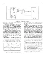
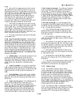
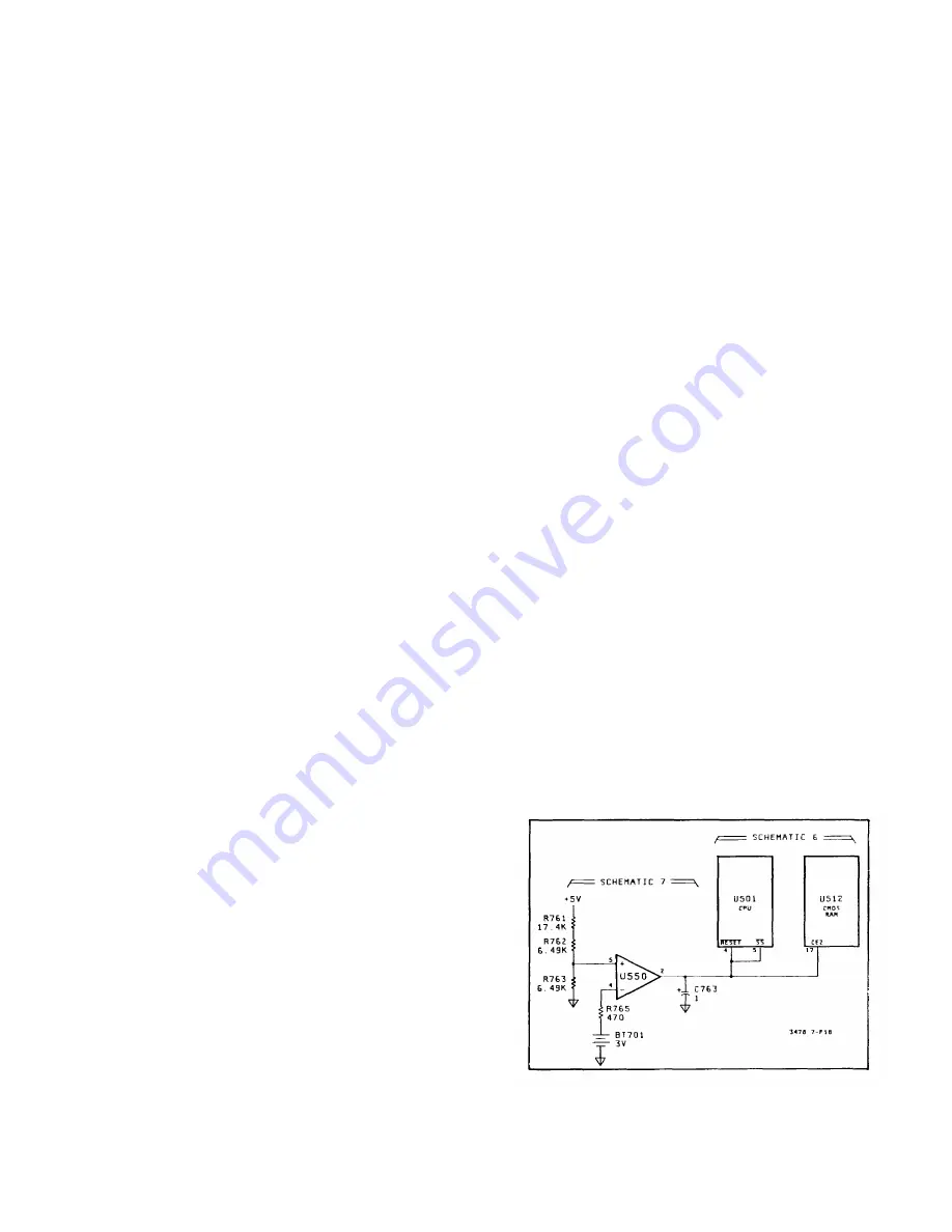
Power-On Circuitry. Refer to Figure 7-F-18, or
Schematic 3 and 4. The Power-On Circuitry resets the
CPU when the 3478A is turned on and when +SV power
supply is low. The step by step operation is as follows:
1.
When the 3478A is turned on, the positive
input of comparator USSOC goes high after the + SV
power supply comes up.
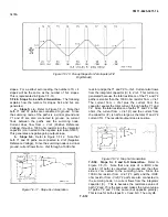
Figure 7-F-18. Power-On Circuitry
7-F-17
Summary of Contents for 3478A
Page 2: ...TM 11 6625 3071 14 A ...
Page 4: ...TM 11 6625 3071 14 C D BLANK ...
Page 12: ...TM 11 6625 3071 14 Table 1 1 Specification 1 2 ...
Page 13: ...TM 11 6625 3071 14 Table 1 1 Specifications Cont 1 3 ...
Page 14: ...TM 11 6625 3071 14 Table 1 1 Specifications Cont 1 4 ...
Page 53: ...TM 11 6625 3071 14 1 ...
Page 54: ...TM 11 6625 3071 14 2 ...
Page 55: ...TM 11 6625 3071 14 3 ...
Page 56: ...TM 11 6625 3071 14 4 ...
Page 87: ...TM 11 6625 3071 14 3478A Figure 7 D 3 Flowchart B 7 D 5 ...
Page 88: ...TM 11 6625 3071 14 3478A Figure 7 D 4 Flowchart C 7 D 6 ...
Page 91: ...TM 11 6625 3071 14 3478A Figure 7 D 6 Flowchart D 7 D 9 ...
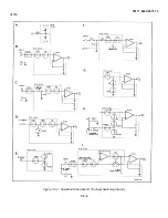
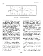
Page 111: ...TM 11 6625 3071 14 Figure 7 F 17 3478A Simplified Reference Circuitry 7 F 16 ...
Page 122: ...TM 11 6625 3071 14 Table A 2 A 2 HP IB Worksheet A 4 ...
Page 137: ...TM 11 6625 3071 14 Figure 7 D 2 Flow chart A 7 D 3 ...
Page 139: ...TM 11 6625 3071 14 Figure 7 G 2 3478A Block Diagram 7 G 3 ...
Page 140: ...TM 11 6625 3071 14 Component Locator for Input Circuitry and Ohms Current Source 7 G 4 ...
Page 141: ...TM 11 6625 3071 14 Figure 7 G 3 Input Circuitry and Ohms Current Source 7 G 5 ...
Page 142: ...TM 11 6625 3071 14 F G 6 ...
Page 143: ...TM 11 6625 3071 14 2 Figure 7 G 4 AC to DC Converter 7 G 7 ...
Page 144: ...TM 11 6625 3071 14 Component Locator for A D Converter and Control Logic 7 G 8 ...
Page 145: ...TM 11 6625 3071 14 3 Figure 7 G 5 A D Converter and Control Logic 7 G 9 ...
Page 146: ...TM 11 6625 3071 14 7 G 10 ...
Page 147: ...TM 11 6625 3071 14 4 Figure 7 G 6 Power Supplies 7 G 11 7 G 12 blank ...
Page 148: ......
Page 149: ...PIN NO 057444 ...

