TM 11-6625-3071-14
3478A
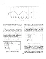
2.
Since the negative terminal of USSOC is
connected to BT701, the output of the comparator
attempts to go high and charges capacitor C763. The
output goes high since the comparator has an open
collector output and a pull-up resistor is connected
between the CPU’s RESET line (output of USSOC and
U5SOD) and + 5V (the resistor is internal to the CPU).
3.
During the charge time, the RESE’I line is
held low until the capacitor is charged to a high level.
4.
The RESET line goes high and the CPU
resets and turns on. The 3478A is now in its turn-on state.
5.
As long as the RESET line is low, the CPU’s
SS (Single Step) line is low (the line is connected to the
RESET line). The SS line steps the CPU to its first
program line. The program line sets the PSEN line high,
which disables the Control ROM (CE high). This prevents
the ROM from operating until the CPU turns on.
6.
When the RESET line is low, the CE2 line of
the CMOS RAM (U512) is also low and disables the RAM
(see paragraph 7-F-61).
7.
The CPU is also reset when the + 5V power
supply goes low. A low + 5V sets the positive in-put of
U550C low which makes U55OC’s output low. This resets
the CPU.
b.
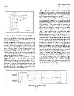
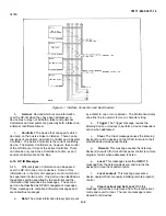
Reset Circuitry. Refer to Figure 7-F-19, or
Schematic 3 and 4. The Reset Circuitry is used to reset
the CPU when the TEST/RESET button is pressed or if
the CPU inadvertently goes to a non-operational state.
The step by step operation is as follows:
1.
During normal operation, counter U507 is
continuously incremented by the ALE clock.
2.
Port P15 (U501 pin 32) continuously output data
Figure 7-F-19. Reset Circuitry
to the keyboard (P15 is one port used to scan the
keyboard, see paragraph 7-F-65). This resets the counter
as long as the keyboard is scanned. The reset pulse is
developed from P15 using C501 and R528.
3.
If the TEST/RESET button is pressed or the
CPU goes to a non-operational state, the keyboard
scanning is stopped.
4.
Since the ALE clock is still operating, the
counter keeps incrementing for about 1.3 seconds.
5.
After the 1.3 seconds, the Q output of U507
goes high (RESET REQ line goes high). This is because
the counter is not being reset.
6.
The Q output is connected to the negative
terminal of comparator U750D. This brings the output of
U750D low which in turn brings the RESET line low.
7.
The ALE clock turns off and the counter
stops incrementing.
8.
The Q output goes low and the output of
U750D attempts to go high and charges C763 (see step a-
2).
9.
Once the capacitor is charged to the high
level, the RESET line once again goes high. The CPU
then resets and turns on. The 3478A is nowin its turn-on
state.
7-F-60. CMOS RAM. The CMOS RAM is used to store
the 3478A’S Calibration Constants. The following
paragraphs explain how the RAM is addressed, how data
(constants) is read from the RAM, and how new data (new
constants) is sent to the RAM. This is done using the
RAM’s Address, Input, and Output Lines. The Address
Lines are connected to the CPU’s lower 8 Address bits
(AO to A7). The RAM’s input and output lines (DO to D3)
are connected to each other and to the DO to D3 Data
Lines.
7-F-61. RAM Addressing. The RAM can only be
addressed as long as line CE2 (Chip Enable 2 at U512 pin
17) is high. The line is high when the 3478A is turned on.
Line CEI (Chip Enable I at U512 pin 19) can be high or
low. This line is used to read the RAM (see next
paragraph).
7-F-62. Reading the RAM. The RAM can be read under
the following conditions.
a. Line OD (Output Disable at U512 pin 18) must be
low. It is low when the RD Line (Read at US01 pin 9) is
low.
b. Line CEI must also be low. It receives the low from
one section of the Quad flip-flop U506 (pin 6).
7-F-18
Summary of Contents for 3478A
Page 2: ...TM 11 6625 3071 14 A ...
Page 4: ...TM 11 6625 3071 14 C D BLANK ...
Page 12: ...TM 11 6625 3071 14 Table 1 1 Specification 1 2 ...
Page 13: ...TM 11 6625 3071 14 Table 1 1 Specifications Cont 1 3 ...
Page 14: ...TM 11 6625 3071 14 Table 1 1 Specifications Cont 1 4 ...
Page 53: ...TM 11 6625 3071 14 1 ...
Page 54: ...TM 11 6625 3071 14 2 ...
Page 55: ...TM 11 6625 3071 14 3 ...
Page 56: ...TM 11 6625 3071 14 4 ...
Page 87: ...TM 11 6625 3071 14 3478A Figure 7 D 3 Flowchart B 7 D 5 ...
Page 88: ...TM 11 6625 3071 14 3478A Figure 7 D 4 Flowchart C 7 D 6 ...
Page 91: ...TM 11 6625 3071 14 3478A Figure 7 D 6 Flowchart D 7 D 9 ...
Page 111: ...TM 11 6625 3071 14 Figure 7 F 17 3478A Simplified Reference Circuitry 7 F 16 ...
Page 122: ...TM 11 6625 3071 14 Table A 2 A 2 HP IB Worksheet A 4 ...
Page 137: ...TM 11 6625 3071 14 Figure 7 D 2 Flow chart A 7 D 3 ...
Page 139: ...TM 11 6625 3071 14 Figure 7 G 2 3478A Block Diagram 7 G 3 ...
Page 140: ...TM 11 6625 3071 14 Component Locator for Input Circuitry and Ohms Current Source 7 G 4 ...
Page 141: ...TM 11 6625 3071 14 Figure 7 G 3 Input Circuitry and Ohms Current Source 7 G 5 ...
Page 142: ...TM 11 6625 3071 14 F G 6 ...
Page 143: ...TM 11 6625 3071 14 2 Figure 7 G 4 AC to DC Converter 7 G 7 ...
Page 144: ...TM 11 6625 3071 14 Component Locator for A D Converter and Control Logic 7 G 8 ...
Page 145: ...TM 11 6625 3071 14 3 Figure 7 G 5 A D Converter and Control Logic 7 G 9 ...
Page 146: ...TM 11 6625 3071 14 7 G 10 ...
Page 147: ...TM 11 6625 3071 14 4 Figure 7 G 6 Power Supplies 7 G 11 7 G 12 blank ...
Page 148: ......
Page 149: ...PIN NO 057444 ...


