TM 11-6625-3071-14
3478A
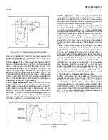
comparators U468A and U468B. The comparators are
used to bring the low level output of T501 up to a TTL
level. The output of the comparators is applied to the TO
input of U462 (U462 pin 1), which is the same data as
the data sent by US01. This makes the output waveform
of U501 the same as the input waveform of U462.
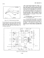
7-F-74. Serial data from U462 to U501 is sent using
drivers U467A and U467B, transformer T401, and
comparators USSOA and USSOB. The circuitry
operation is the same as sending data from U501 to
U462 (see previous paragraph). The difference is that
the data is input to the TI line of USO1 (USO1 pin 39)
instead of TO, as is the case with U462.
7-F-75.
Floating Common Logic Circuitry
7-F-76. The main parts of the Floating Common Logic
Circuitry are the A/D Controller and the A/D Converter.
The A/D Controller consists of CPU U462 and the A/D
Converter is U403 and associated circuitry. Other
circuitry includes an Digital to Analog Converter (U465
and associated circuitry) and a Voltage Reference
Supply (U404, U405, and U461). For the explanation on
the A/D Converter and Voltage Reference refer to
paragraph 7-F-49. The operation of the A/D Controller,
the Digital to Analog Converter, and other logic circuitry
is explained in the following paragraphs.
7-F-77.
A/D Controller (U462) Operation. The
purpose of U462 is to control the A/D operation, set up
the Digital to Analog Converter, and to send set-up
(Range and Function) information to the Input Hybrid
U102 (see paragraph 7-F-13 for its operation and
purpose). The CPU also determines measurement data
from the A/D Converter and sends the data (readings) to
the Chassis Common CPU (USO1). The CPU (U462)
has an internal 128 bytes of RAM memory, 2K bytes of
ROM memory, and a clock. The frequency and stability
of the clock is determined by a 10.98MHz crystal Y460.
The ROM is used to control the CPU operation and the
RAM is used to store Autozero constants (see paragraph
7-F-14). Since the U462 has an internal ROM, all
addressing and data transfer is done using bi-directional
Ports P10 to P17 (U462 pins 27 to 34) and P20 to P27
(U462 pins 27 to 34, 21 to 24, and 35 to 38).
7-F-78.
A/D Converter Control. The A/D Converter
receives control data from the CPU Ports P10O to P14
(U462 pins 27 to 31). The data is used to select the
various slopes (see paragraph 7-F-49) in the converter.
The output of the A/D Converter (CMP, the Comparator
Output) is applied to the Ti input of the CPU (at U462 pin
1). The ALE output (Address Latch Enable at U462 pin
11) is used as the converter’s clock. Refer to paragraph
7-F-31 for more information on the A/D operation.
7-F-79.
Input Hybrid Control. The control lines to the
Input Hybrid (U102) which come from Ports P15 to
P17of the CPU and are: Data, Mode, and Clock. The
lines do the following:
a. When the Clock input (U102 pin 24) is low, no
data is transferred into the hybrid.
b. When the clock input is high, the following occurs:
1. When the Mode input (U102 pin 25) is low, data
on the Data line (U102 pin 26) is transferred into the
hybrid (into an internal shift register).
2. When the Mode input is high, the data in the
hybrid (in its shift register) is used to set-up the switches
in the hybrid.
7-F-80. Digital to Analog Converter Operation. The
3478A’s A/D Converter requires a certain offset voltage
(see paragraph 7-F-46 for more information). This offset
is applied to the negative input of the A/D Integrator
(U401) and comes from the Digital to Analog Converter
(DAC). The offset voltages are developed by resistors
R401 to R406, which are selected by Hex D flip-flop
U465. Each time the flip-flop is clocked by the ALE line,
its QO to Q5 outputs are set either high or low. This
depends on the position (high or low) of Ports P20 to
P25. The outputs in conjunction with resistors R401 to
R406 generates a certain offset voltage.
7-F-81.
CPU Reset Operation. The Chassis Common
CPU (US01) can reset the Floating Common CPU
(U462) whenever needed. This is normally done when
the 3478A is turned on. The operation is as follows.
a.
Counter U466 increments each time it is
clocked by the ALE line (U462 pin 11).
b.
As long as the Chassis Common sends data
bytes over the Isolation logic, the counter is reset each
time the data byte has a high (a high resets the counter).
c.
If the counter’s Reset line stays low (e.g. no
high level from the data bytes), the counter keeps on
incrementing for about 11mS. The counter’s Q14 output
then goes high.
d.
The Q14 output is inverted by NOR gate
U467C (connected like an inverter) and sets the CPU’s
RESET line (U462 pin 14) low. The CPU turns off.
e.
The CPU remains off until the counter’s Reset
line receives a high from the data bytes. This resets the
counter and its Q14 output goes low. The RESET line of
the CPU goes high and U462 resets and turns on to a
predefined condition.
7-F-82.
Front/Rear Switch Position. The 3478A’s
Front/Rear Switch position is determined by the state
(high or low) of Port P26. A low state is when the port is
7-F-21
Summary of Contents for 3478A
Page 2: ...TM 11 6625 3071 14 A ...
Page 4: ...TM 11 6625 3071 14 C D BLANK ...
Page 12: ...TM 11 6625 3071 14 Table 1 1 Specification 1 2 ...
Page 13: ...TM 11 6625 3071 14 Table 1 1 Specifications Cont 1 3 ...
Page 14: ...TM 11 6625 3071 14 Table 1 1 Specifications Cont 1 4 ...
Page 53: ...TM 11 6625 3071 14 1 ...
Page 54: ...TM 11 6625 3071 14 2 ...
Page 55: ...TM 11 6625 3071 14 3 ...
Page 56: ...TM 11 6625 3071 14 4 ...
Page 87: ...TM 11 6625 3071 14 3478A Figure 7 D 3 Flowchart B 7 D 5 ...
Page 88: ...TM 11 6625 3071 14 3478A Figure 7 D 4 Flowchart C 7 D 6 ...
Page 91: ...TM 11 6625 3071 14 3478A Figure 7 D 6 Flowchart D 7 D 9 ...
Page 111: ...TM 11 6625 3071 14 Figure 7 F 17 3478A Simplified Reference Circuitry 7 F 16 ...
Page 122: ...TM 11 6625 3071 14 Table A 2 A 2 HP IB Worksheet A 4 ...
Page 137: ...TM 11 6625 3071 14 Figure 7 D 2 Flow chart A 7 D 3 ...
Page 139: ...TM 11 6625 3071 14 Figure 7 G 2 3478A Block Diagram 7 G 3 ...
Page 140: ...TM 11 6625 3071 14 Component Locator for Input Circuitry and Ohms Current Source 7 G 4 ...
Page 141: ...TM 11 6625 3071 14 Figure 7 G 3 Input Circuitry and Ohms Current Source 7 G 5 ...
Page 142: ...TM 11 6625 3071 14 F G 6 ...
Page 143: ...TM 11 6625 3071 14 2 Figure 7 G 4 AC to DC Converter 7 G 7 ...
Page 144: ...TM 11 6625 3071 14 Component Locator for A D Converter and Control Logic 7 G 8 ...
Page 145: ...TM 11 6625 3071 14 3 Figure 7 G 5 A D Converter and Control Logic 7 G 9 ...
Page 146: ...TM 11 6625 3071 14 7 G 10 ...
Page 147: ...TM 11 6625 3071 14 4 Figure 7 G 6 Power Supplies 7 G 11 7 G 12 blank ...
Page 148: ......
Page 149: ...PIN NO 057444 ...

