background image

Scanned by KN5U

Reproduced with permission, 

Courtesy of Agilent Technologies Inc. 

Summary of Contents for 5335A

Page 1: ...Scanned by KN5U Reproduced with permission Courtesy of Agilent Technologies Inc ...

Page 2: ...Scanned by KN5U Reproduced with permission Courtesy of Agilent Technologies Inc ...

Page 3: ...Scanned by KN5U Reproduced with permission Courtesy of Agilent Technologies Inc ...

Page 4: ...tallation Procedures for Option 030 2 35 Field Installation Procedures for Option 040 2 37 Storage and Shipment 2 38 Environment 2 41 Packaging III OPERATION AND PROGRAMMING 3 1 Introduction 3 4 Operating Characteristics 3 7 Local Operation 3 10 Remote Operation 3 12 Operator s Self Check Procedure 3 14 General Operation Information 3 15 Power Up Self Check 3 19 Display 3 26 Keyboard 3 28 Key Indi...

Page 5: ...ASE A rei B 3 20 Special Functions 3 21 Programming 3 22 Introd uction 3 22 Interface Function 3 22 Bus Messages 3 23 Address Selection 3 25 Device Command Definitions 3 26 Programming 5335A Option 040 3 27 Trigger Level Setting TR AT BT 3 27 The 5335A Device Commands 3 27 Function Selection FU FN 3 31 Gate Time Setting GA GO GC 3 31 Remote Display DR0 DR1 DI 3 31 Default States 3 31 Initialize 3 ...

Page 6: ...II Performance Test for the 5335A and All Options Power Up Self Check Test Procedure I Supercheck Test Procedure II Keyboard Check Test Procedure III Rear Panel External Arm Switch Test Procedure IV Gate Time Test Procedure V Channel A and B Frequency Response and Sensitivity Test Procedure VI Ratio A B Function Test Procedure VII Time Interval and Inverse Time Interval Test Procedure VIII Pulse W...

Page 7: ...6 5 Replaceable Parts 6 9 Ordering Information 6 12 Direct Mail Order System VII MANUAL CHANGES 7 1 Introduction 7 3 Manual Changes 7 6 Older Instruments 7 8 Selected Components A3 Series 2120 or Below 7 10 Procedure for Selecting R7 R8 R80 or R81 in A3 Assembly VIII SERVICE 8 1 Introduction 8 3 Schematic Diagram Symbols and Reference Designators 8 5 Reference Designations 8 7 Identification Marki...

Page 8: ... 12 Programmable Input Amplifier Option 040 A 15 Temperature Controlled 10 MHz Time Base Oscillator Option 010 Troubleshooting Failure Analysis Built In Diagnostics Introduction Accessing the Built In Diagnostics Shaded Block Diagrams Diagnostic 1 Super Check Diagnostic 2 Signature Analysis Stimulus Mode Diagnostic 3 and 4 Front End Latch Control Test Diagnostic 5 Front End Switch Test Diagnostic ...

Page 9: ...ting Peak Detectors Troubleshooting A3 Troubleshooting Accessories A3 Troubleshooting Out of Cabinet Setup Peak Detectors in Manual Mode Troublelshooting Peak Detectors in Auto Mode Troubleshooting Schmitt Amplifier Troubleshooting Bridge Limiter Troubleshooting A4 Main Logic Troubleshooting Microprocessor System Troubleshooting Troubleshooting the A4 Assembly Using STIMULUS MODE and Signature Ana...

Page 10: ...g 8 87 8 476 Trigger Level Selector Troubleshooting 8 87 8 479 Front End Latch Control Troubleshooting 8 87 8 484 Troubleshooting the Al1U5 Multiplexer 8 87 8 488 Troubleshooting the Relay Drivers 8 88 8 490 Digital to Analog Converter Troubleshooting 8 88 8 496 Troubleshooting the Data Latch Enablers U19 and U20 8 88 8 500 Trigger Level Voltmeter Troubleshooting 8 89 8 507 Signal Selector Multipl...

Page 11: ...justments Abbreviations and Reference Designations Replaceable Parts Miscellaneous Replaceable Parts Option 020 DVM Replaceable Parts Option 030 C Channel Replaceable Parts Option 040 Programmable Input Replaceable Parts Manufacturers Code List 4 1 4 1 4 21 4 34 4 41 5 1 5 6 5 9 6 2 6 3 6 17 6 28 6 30 6 32 6 40 7 1 Manual Backdating 7 1 7 2 A6 05335 60006 Series 1928 Replaceable Parts 7 5 7 3 A3 S...

Page 12: ...in Diagnostics 20 25 8 84 A8 Voltage to Frequency Conversion 8 84 A8 Input Logic Switching Troubleshooting 8 85 A11U2 Analog Multiplexer Control Bits 8 87 Troubleshooting A11U14 and A11U15 8 87 A11U5ControiSignais 8 88 A11 Relay Driver Collector Voltages 8 88 A11 Data Latch Logic Levels 8 88 A2U4 Analog Multiplexer Control Bits 8 90 Input Voltage vs Output Frequency 8 90 A 11U7 Outputs Related to ...

Page 13: ...r J1 and Fuse Mounting 5335A Operating Instructions Label Front End Input Switch Test Display Rear Arm Switch Test Display Keyboard Check Key Assignments Option 040 DAC Test Setup Keyboard Check Key Assignments Rear Arm Switch Test Display Channel A Frequency Response and Sensitivity Test Setup 20 MHz Channel A Frequency Response and Sensitivity Test Setup 200 MHz Channel B Frequency Response and ...

Page 14: ...r A6 05335 60006 Series 1928 Schematic Diagram Al3 Part Number 0960 0448 Schematic Diagram Schematic Diagram Notes Test Setup for A3C37 and C23 Selection Symbol Composition Illustration of Common Control Block Illustration of Common Output Element G Dependency Between Inputs G Dependency Between Outputs and Inputs G Dependency with A Dynamic Input OR ed Affecting inputs Substitution for Numbers V ...

Page 15: ...Diagram 8 38 Diagnostic 02 Shaded Block Diagram 8 40 Diagnostic 05 Shaded Block Diagram 8 41 Diagnostic 05 Display 8 42 Diagnostic 06 Display 8 42 Diagnostic 06 Shaded Block Diagram 8 43 Diagnostic 07 Display 8 44 Diagnostics 07 and 16 Shaded Block Diagram 8 45 Diagnostics 09 and 10 Shaded Block Diagram 8 46 Diagnostics 11 12 and 13 Shaded Block Diagram 8 48 Diagnostic 14 Shaded Block Diagram 8 49...

Page 16: ...ram 8 81 A8 Digital Voltmenter Option 020 Block Diagram 8 83 A9 Channel C Option 030 Block Diagram 8 86 A9 Waveforms at TPl and TP3 8 86 AllU19 and AllU20 Signatures 8 89 Trigger Level DVM Block Diagram 8 89 Signal Select Block Diagram 8 91 Channel A Input Buffer DC Voltages 8 92 Block Diagram of Peak Detectors in All and A 12 8 93 Peak Detectors Test Signal 8 94 A12U6 and A12Ul Pin Voltages 8 95 ...

Page 17: ...introductory types of information and are intended to be used only for reference Where applicable photos illustrations and diagrams foldout allowing the user accessto related information throughout the manual In limiting the depth of coverage in this manual a certain amount of previous knowledge on the part of the reader must be assumed A variety of additional related documentation is avail able T...

Page 18: ...ides primary operating instructions and service information 5335A USER S GUIDE Provides expanded operating instruction and instrument specific applications FUNDAMENTALS OF ELECTRONIC COUNTERS AN 200 Provides the basic concepts techniques and underlying principles of electronic counters HP 8725A HP IB PROGRAMMING HINTS Includes a variety of HP IB related documents including general bus theory and i...

Page 19: ...10 CRYSTAL OSCILLATOR 10811 60111 OR 10544 60011 88888 5 t 8ilil8 __ L J OPTION 030 OPTION 020 CHANNEL C DVM v OPTION 040 PROGRAMMABLE INPUT POWER CORD PART NO 8120 1378 1 0 Figure 1 1 Model 5335A Universal Counter with Option 040 Option 030 Option 020 Option 010 and Accessories Supplied Scanned by KN5U Reproduced with permission Courtesy of Agilent Technologies Inc ...

Page 20: ...ering information for all replaceable parts and assemblies within the instrument SECTION VII MANUAL CHANGES This section con tains manual change information which effectively backdates the technical areasof the manual to apply to older instruments SECTION VIII SERVICE This section provides the instrument theory of operation troubleshooting in formation repair techniques and schematic diagrams 1 5 ...

Page 21: ...IS to 4s NOMINAL for gate modes of Fast Norm and Manual Delay measured by pressing Gate Time key All other specifications are same as Time Interval A B INVERSE TIME INTERVAL A B Range 10 7 to 10 units second LSD Displayed Resolution and Accuracy are inverse of Time Interval A B specifications If Time Interval A B is zero display will be zero RISE AND FALL TIME A Range 20 ns to 10 ms Minimum Pulse ...

Page 22: ...e Hold Freezes decimal point and exponent of display Reset Starts a new measurement cycle when pressed Check Performs internal self test and lamp test Display 12 digit LED display in engineering format exponent range of 18 to 18 Overflow All measurements which would theoretically cause a display of more than 12 digits will display 12 most significant digits Operating Temperature 0 to 50 C Power Re...

Page 23: ...c to 5V de Coupling AC Impedance 50 n NOMINAL VSWR 2 5 1 TYPICAL Damage Level V DC AC peak fuse protected Fuse located in BNC connector Frequency C Range 150 MHz to 1 3 GHz prescaled by 20 LSD Displayed Resolution and Accuracy are same as Frequency A DEFINITIONS Trigger Level Setting Error Xl Applies to Rise Fall Slew and Phase measurements 2 of input POpvoltage 40 mV Input slew rate at trigger po...

Page 24: ...35A input provides two independent channels featuring matched high performance 200 MHz input amplifiers Each input channel includes a full complement of input signal conditioning controls Additionally the 5335Aoffers extensive control of trig gerring and arming Most measurements are displayed in scientific notation with the digits grouped into three s for convenience Four modes of gate selection a...

Page 25: ...Drawer 1 82936A OV HP IB Interface 1 82937A OV Function Generator 3312A A P OV Signal Generator 200 MHz bandwidth 1 8654A1B OV P son RF Termination SMC type 2 1250 0839 T Synthesized Signal 1300 MHz 150 mV rms 1 8660B 86603A A OV P Generator Front Panel switch 1 5020 8160 T replacement tool heat stacking tool Flat Ribbon assembly 26 AWG 18 conductors 2 8120 2463 T 50 ohm cable assembly 2 05335 601...

Page 26: ...Power line connections are selected by the position of the plug in pc selector card in the module When the card is plugged into the module the only visible markings on the card indicate the line voltage to be used The correct value of line fuse must be installed after the card isinserted This instrument uses a power line fuse as listed in Section VI 2 11 To convert from one line voltage to another...

Page 27: ...l HP IB connector is provided in Figure 2 3 This connector is compatible with the HP 10631A B C D HP IB cables The HP IB system allows interconnection of up to 15 including the controller HP IB compatible instru ments The HP IB cables have identical piggyback connectors on both ends so that several cables can be connected to a single source without special adapters or switch boxes System component...

Page 28: ...each other or the threads of either or both will be destroyed Metric threaded HP IB cable hardware illustrations and part numbers follows LONG MOUNTING SHORT MOUNTING STUD STUD 0380 0643 0380 0644 Logic Levels The Hewlett Packard Interface Bus logic levels are TTL compatible i e the true 1 state is O OVdc to O 4V dc and the false 0 state is 2 5V dc to 5 0V dc Programming and Output Data Format Ref...

Page 29: ... 14 e Disconnect the power cable from the 5335A 2 4 f Plug the oven oscillator 10544 60011or 10811 60111 into A4XA15 and secure oven oscillator to A4 assembly from underneath with two screws 6 32 X 5 16 and fiber washer provided PIN 3050 0005 g Restore top and bottom covers to the 5335A h Apply power to the 5335A and verify counter operation by performing the operational verification in Section IV...

Page 30: ...X 1 4 Screws 2360 0113 3 2 32 Field Installation Procedures For Option 030 2 33 To install Option 030 order parts listed in Table 2 1 or order Retrofit Kit 05335 60230 then proceed as follows a Disconnect power cable from the 5335A safety precaution b Remove top and strapped sided cover of the 5335A c Remove blank panel by removing the two 5 16 inch hex nuts that holds blank panel to the mainframe...

Page 31: ...dard module isdescribed in step a If Option 020 DVM and or Option 030 C channel is REMOVABLE BNC BARREL 05305 60205 NOTE USE A BNC CONNECTOR TO REMOVE AND TIGHTEN THE FUSE BARREL installed they MUST be removed before installing Option 040 reverse the stepsof the option s installation procedures as outlined in previous paragraphs Also refer to Figure 8 22Assembly and Cable Locator during this insta...

Page 32: ...e 5335A front flange ModelS33SA Installation b Installation of Option 040 1 Attach Al0 keyboard assembly to the AS dis play board by connecting Al0n to ASJ2 2 Insert the ASIA10 assembly combination into the S335A front flange and attach the thirteen retai ner c1ips that fixes ASIA 10 to the front flange 3 Position the Al0 assembly such that the mo mentary switches are centered with their re specti...

Page 33: ...er and full serial number 2 8 2 43 OTHER PACKAGING The following general instructions should be used for repacking with com mercially available materials a Wrap instrument in heavy paper or plastic If shipping to Hewlett Packard office or service center attach tag indicating type of service required return address model number and full serial number b Use a strong shipping container A double wall ...

Page 34: ...r level and low pass filter controls Low PassFilters have been added to the input buffer circuits These are selectable via the front panel or the HP IB Front panel INPUT controls are momentary pushbutton keys with inset LED indicators to represent status 3 7 LOCAL OPERATION 3 8 The local operation vice remote operation of the HP 5335A is presented through the following subsections GENERAL OPERATIO...

Page 35: ...ht momen tarily followed by the momentary display of the instrument s decimal HP IB address e g HP IB Addr 28 3 17 After the power up sequence the counter will initialize itself All math and statistics will be off the function will be Frequency A and the gate and cycle modes will be in Norm All of the input controls will be set according to their switch positions 3 18 Any failures during the power...

Page 36: ... from the keys labeled in blue Refer to paragraph 3 82 3 30 Keyboard Memory 3 31 To avoid having to reenter math constants etc whenever switching between two functions repeti tively the keyboard has one level of memory This allows you to set up two functions modes each with their own set ups The key set ups for each of the keys in the MATH STATISTICS FUNCTION GATE and CYCLE groups are automaticall...

Page 37: ...ack are directly accessible from the four leftmost columns of keys The indicator LED within the key identifies which one of the functions is active Several more functions are available accessed through the HP IB and other means see Special Function Mode paragraph 3 35 and Diagnostics in Section VIII During the programming sequence for the MATH group the functions of these 16 keys and CHECK are rea...

Page 38: ...e is MIN if no delay is desired For more information about the GATE ADJ control during time domain measurements refer to TIME A B paragraph 3 115 Figure 3 2 shows the GATE and CYCLE controls 3 50 Gate mode NORM and FASTare two ranges of adjustable gate times NORM has a range of nominally 20 milliseconds to 4 seconds and FAST has a range of nominally 100 microseconds to 20 milliseconds The one key ...

Page 39: ...e addition of Option 040 affects only the INPUT section of the front panel controls The INPUT group contains the A Channel and B Channel input BNC connectors signal conditioning and triggering controls The operation of all the pushbutton keys within this section is the same The keys operate in a toggle on toggle off fashion An indicator LED in the center of each key represents the keys status A st...

Page 40: ...splay by 10 when a X10attenuator ison When X1 is selected the input signal not attenuated and the key indicator LED will be unlighted When X10 is selected the input signal is attenuated by ten and the key indicator LED will be lighted Model 5335A Operation and Programming 3 74 Triggering MANUAL AUTO 3 75 The HP 5335A has an extensive set of triggering features which make accurate measurements on i...

Page 41: ...ions on the measurement before it isdisplayed The OFFSET NORMLZ and SCALEkeys allow for the addition division and multiplication respectively of the measurement by user specified constants Modi fication of the display by the Math operations is represented by the following relationship Measurement OFFSET Display N O R M LZ X SCALE 3 84 Notice that the OFFSEToperation is performed before normalizati...

Page 42: ...s an example of MEAS t 1 with OFFSET As with LAST DISP the value is negated for OFFSET and not for NORMLZ and SCALE 3 86 REVIEWING CONSTANTS To review the con stants press any of the blue keys The counter will cease taking measurements and the presently spec ified value of the constant will be displayed The indicator light within the blue key specified will be flashing At this time either the valu...

Page 43: ...lue 1005 Hz Displayed value 3 Hz More precise timi ng of the gate can be achieved by arming 3 91 STATISTICSGroup 3 92 The functions within the STATISTICS group allow the user to automatically accumulate and sample 100 or 1000 measurements and then determine and display either the standard deviation or the mean average of the sampling These functions are selected by the STD DEV and MEAN keys respec...

Page 44: ...Scanned by KN5U Reproduced with permission Courtesy of Agilent Technologies Inc ...

Page 45: ...Scanned by KN5U Reproduced with permission Courtesy of Agilent Technologies Inc ...

Page 46: ...intent of the fol lowing paragraphs is to provide an instructional discussion which demonstrates the user control flexibility for each major function mode These oper ating guidelines should assist in making the most useful and accurate measurement possible 3 108 FREQ A Channel A Frequency 3 109 The FREQ A mode makes measurements on frequencies up to 200 MHz through the Channel A INPUT In this func...

Page 47: ...these types of signals tends to distort them slightly due to the charging of the coupling capacitor Additionally the position of the signal on the zero preset trigger level is determined by the average dc level of the input Depending on the pulse width and duty cycle this dc average may be low enough to allow the base line noise to trigger the counter producing extra counts Figure 3 18 shows AC co...

Page 48: ...sired points issimplified by using AUTO TRIG however the input signal to Channel A should be continuous The selected trigger levels may be viewed by pressing the TRIG LVL key or monitoring the rear panel trigger level outputs For rise time measure ments using the 10 and 90 points see RISETIME A Figure 3 27 shows voltage rise time measurement 3 120 The T I DELAY time interval delayed mode is useful...

Page 49: ...DE set to NORM or FAST the totalize acts somewhat like a frequency measure ment Based on the CYCLE and ARM modes the totalizing will start and stop without the need for manual operation Also between measurements the count will automatically reset itself 3 125 To totalize the number of events in a burst of pulses which occur at one second intervals set the GATEMODE to NORM Adjust the GATEADJ contro...

Page 50: ...actor of 20 however aswith FREQ A there is no loss of resolution When FREQ C is selected the Channel A and B INPUT section is Model 5335A Operation and Programming disabled Measurements through C Channel respond to all other controls the same asFREQA measurement 3 132 1 TIME A 8 3 133 The llTlME A B mode performs the standard TIME A B measurement mathematically computes the reciprocal value and di...

Page 51: ...A Channel A Rise and Fall Time Measurement 3 143 The RISE FALL A mode automatically con figures the counter to perform either rise or fall time measurements The input is automatically setto COM A and triggering to AUTO TRIG In this mode AUTO TRIG automatically locates and sets the trigger levels at the 10 and 90 points of the input signal Rise time measurements are made when the SLOPE A control is...

Page 52: ... gate time resolution to 100 ns is displayed The gate time is controlled except in MIN by the GATEADJ control NOTE As the gate is synchronized to the input signal the actual gate time may be different from the displayed gate 3 152 When in a TIME domain function mode e g TIME A B PULSEA the GATE TIME mode provides an indication of the amount of stop delay time selected This time is set by the GATE ...

Page 53: ...360 If RANGE HOLD is on the range is fixed to 0 to 360 The PHASEmode cannot be externally armed Figure 3 32 shows waveform phase relationships 3 163 Phase measurements are made through a series of individual measurements therefore certain input and operational restrictions apply The frequency and phase angle of the signals should be constant Frequencies can be measured up to 1 MHz 3 20 PHASEA rei ...

Page 54: ... arming MIN only Needs constant signal Range 00 to 3600 if RANGE HOLD on 30 Hz 3 164 SPECIAL FUNCTIONS 3 165 Functions 17 18 19 and 20 are additional functions that are available in the 5335A 17 FREQ B 18 TIME B A 19 TOT A B 20 PULSE B These functions are accessed via the HP IB through the normal FN or FU command however they may also be accessed manually through the keyboard This is an example of...

Page 55: ...s the 5335A Interface Functions using the termi 3 22 nology of the IEEE488 1978standard These features are also listed below the rear panel HP IB connector as follows SH1 AH1 T1 TE0 L2 LE0 SR1 RL1 PP0 DC1 DT1 C0 Table 3 3 HP IB Interface Capability INTERFACE FUNCTION SUBSET IDENTIFIER INTERFACE FUNCTION DESCRIPTION SH1 Complete source handshake capability AH1 Complete acceptor handshake capability...

Page 56: ...iversal or selected device clear is re ceived the instrument clears out all input buffers Model 5335A Operation and Programming and resets the hardware for a new measurement The display will flash momentarily SRQ is also cleared Device clear can be used to clear an ERROR message DEVICE TRIGGER When a device trigger is received a new measure ment is started CONTROLLER No controller capability in th...

Page 57: ...g states are invoked WA0 DR0 and SR0 Local Disables local front panel Disables front panel RESET 1107 LOCAL LOCKOUT 7 or Lockout controls fo selected devices 5335A remains in remote LOCAL LOCKOUT 703 Clear Returns all devices to local Local Lockout cleared and re Ici 7 LOCAL 7 Lockout front panel control and turns to local front panel and Local sirnu Itaneously clears the Local control Lockout Mes...

Page 58: ...lator since the calculator addresses the 5335A to talk and listen by using the code 703 The 03 being the 5335A address The ASCII characters for this same switch setting are C for a talk address and for a listen address These characters are used when the comput ing controller is an HP 9830A calculator Table 3 5 HP IB Address Switch Selections INSTRUMENT TALKONLV NOTE I A A I B THE TALK ONLY SWITCH ...

Page 59: ... 123456 OUTPUT 7 3 REMS l 23456E 05 OUTPUT 7133 RE MS123 456E3 S 123456 OUTPUT 7133 RE MS Scale OUTPUT 7133 RE MS123 456E3 123456 A wrt 7133 RE MS A wrt 7133 RE MSl23 456E3 2 Binary Command Type B A sequence of two ASCII coded bytes followed by either a 13 or a 1 The 13 indicates the selected function if OFF or FALSE and the 1 or any non zero value indicates ON or TRUE The binary command uses the ...

Page 60: ... and sending itthe desired device commands Table 3 6 shows the device commands for the Option 040 Programmable Input Amplifiers The first section contains the standard device commands which remain unchanged and the second section liststhe added commands with Option 040 NOTE It is necessary to send the TRO TRIG REMOTE command prior to an AU1 AUTO TRIGGER or AP1 BP1 PRE SET command 3 187 The 5335A D...

Page 61: ...100 1K Set N 100 B SNB Set N 1000 B SN1 STD DEV Disable Standard Deviation B SOB Enable Standard Deviation B SD1 MEAN Disable Mean B 5MB Enable Mean B SM1 SMOOTH Disable Smooth B SSB Enable Smooth B SS1 SPECIAL OUTPUT Special Output disable B SOB Special Output enable B S01 FUNCTION ALL FUNCT Select Function I FU I FN FREQ A Standard Functions FN1 TIME A B FN2 TOT A FN3 RATIO AlB FN4 FREQ C FN5 1 ...

Page 62: ...EXT STOP External STOP Arm Slope Positive I XOl External STOP Arm Off I X02 External STOP Arm Slope Negative I X03 DISPLAY DISP REMOTE Set display to NORMAL B DRO Set Display to REMOTE B DRl blank display DISP DATA Display data with display in Remote N DI BINARY Request Request 30 byte binary status T P Request 30 byte binary status T PQ Program Program with binary status PB MISC Wait WAIT to send...

Page 63: ...t B to AC B BAl TRIG ADJ Set TRIGGER LEVELA N AT Set TRIGGER LEVEL B N BT TRIG REMOTE Set TRIGGER LEVELSto LOCAL B TRO Set TRIGGER LEVELSto REMOTE B TRl Where is the trigger level value from 5 00 to 5 00 programmed in the format AT X XX For example a plus two volt trigger level can be AT2 AT2 AT 2 AT 2 0 or AT 2 00 3 189 Commands may be sent upper or lower case To separate commands you may use not...

Page 64: ... by the 01 command 12345 to be formatted into engineering notation and dis played With the display in remote normal measure ments can still be programmed executed and output through the HP IB but the results will not be dis played Model 5335A Operation and Programming 3 196 Default States 3 197 The default state is equivalent to sending all commands with a parameter of zero This may be different f...

Page 65: ...nciator 3 208 The 5335A will only send SRQ if a measure ment is ready for sending and it is in the WAIT mode and it is not addressed to TALK or RFD is false Measurement done AND SRQ if in WAIT mode AND if not addressed to TALK or RFD is false NOTE Constant reading of the status byte is not recommended This may slow down the measurement processor time 3 209 Program Execution Response Times 3 210 Pr...

Page 66: ... which specify the type of measurement It is generally used to indicate the type of units The alpha characters are F precedes Frequency measurements units of Hz Hertz S precedes Time measurement units of s seconds V precedes Voltage measurements units of V Volts R precedes Ratio measurement no units T precedes Totalize measurements no units sp precedes 1 TIME DUTY CYCLE PHASE units as specified A ...

Page 67: ...o monitor the 5335A for the end of measurement occurrence This bit is effective only if the WAIT mode is ON 3 222 When receiving trigger level data it is recom mended that the WAIT mode be ON This will assure no loss of data However the TRIG LVL function is 3 34 unique in that it does not show a display until after it outputs to the HP IB Therefore the WAIT mode should be turned OFF if you want th...

Page 68: ...easurement into string A and then step 3 displays the information After waiting for 1 second 1000 milliseconds the program loops back into reading a new measurement and the cycle is repeated Model 5335A Operation and Programming 9825A EXAMPLE n cI i 1 1 I t 1 1 l 1 t t 0 3 II in 1 a II cI O 1 I 3 d sp 1 I 4 I Ji i I l 0 l 1 q t 0 _ 3 E nci 24 S6 HP 85 EXAMPLE 10 DIM A 21 20 OUTPUT 703 lin ga 5 30 ...

Page 69: ... the 5335A for a Pulse A r measurement fu7 in step 5 In step 6 the 5335A will read into the simple variable B Step 7 will display the contents of variable B formatted as follows PULSE A s Following 3 seconds of waiting the whole process is repeated 9825A EXAMPLE 0 I Jr 03 I i n FI J C I h ii i 1 d 03 A f I t d p II T 1 II 1 II f C II 4 J l i t 3000 r I J t 0 3 II i n f I II 6 t od 03 B i eI P PUI ...

Page 70: ...t o 1 0 1 1 cI I H 7 7 1 Model 5335A Operation and Programming up for a Negative Slew Rate A in step 14 and the con troller reads this information into variable B in step 15 then the 9825A will show the contents of B along with the display NEG SLEW RATE V IS in step 16 after which the whole process is repeated HP 85 EXAMPLE 10 CLEAR OUTPUT 703 in fu10 20 WAIT 3000 30 ENTER 703 A 40 IMAGE RISE TIME...

Page 71: ... pI t n pc 9 p r 1 II SC H J II 3 1 f p c 1 wr 1 1 6 RF UI T 12 wrt 16 AS i1t11AS S 191 1 3 nd t il j i 1 1 I ClFF T i U N W riAL J zs N CAI E 0 3 i i n 1f 0 II v ln II N II MS 03 i A I OFF T II 0 II 3 II NDI MAL J lE II iN 9825A PRINTED RESULTS to t f CFL E HP 85 EXAMPLE 10 DIM A 21J 20 CLEAR 30 IMAGE OFFSET 6D 3D 40 IMAGE NORMALIZE 6D 3D 50 IMAGE SCALE 6D 3D 60 DISP ENTER OFFSET FACTOR INPUT O 7...

Page 72: ...sent to the 5335A display in step 3 The cycle is again repeated in step 4 HP 85 EXAMPLE 10 OUTPUT 703 fuldr1 20 ENTER 703 A 30 B A 1000000 40 OUTPUT 703 di B 45 WAIT 2000 50 GOTO 10 60 END front panel settings of the counter steps 10 and 11 Also it will allow the user to suppress the MATH in formation and thereby speeding up the transfer of data steps 12 13 and 14 Note however that the OFFSET NORM...

Page 73: ...ESS CONTI WHEN READY 40 PAUSE 50 OUTPUT 703 pq 60 ENTER 703 USING n 30A A 61 LOCAL 703 62 BEEP 80 DISP NOW CHANGE THE 5335A CONTROLS PRESS CONTI WHEN READY 90 PAUSE 100 DISP DO YOU NEED MATH FUNCTIONS Y 1 N O 105 INPUT B 110 IF B O OR B 1 THEN 100 115 IF B THEN 170 120 OUTPUT 703 USING 2A 6A B pb A 255 130 BEEP 140 WAIT 500 150 BEEP 160 GOTO 210 170 OUTPUT 703 USING 2A 30A pb A 180 BEEP 190 WAIT 5...

Page 74: ...r a Standard Deviation measurement and it will store the result in the two string variables step 11 in steps 12through 25 the 9825A will print the contents of the variables with appropriate identification 9825A EXAMPLE 0 diM AS 2il BSr2il CS 2il i f nt Sar lplf SiZE 1 00 1000 N O 1 N 2 W7 t 70 3 I i nsn N M i 1 3 red 703 A B C 4 p r t FI FClJ NCY A S pr t STAT Il TI C 5 p r 7 p 7 t 1 EAN 8 wrt 16 ...

Page 75: ...1 20 CLEAR DISP Sample size 100 1000 N O 1 25 INPUT N 30 OUTPUT 703 insn N sm1 sol 40 ENTER 703 A B C 50 CLEAR DISP FREQUENCY A STATISTICS 70 DISP USING 2 80 DISP MEAN A DISP 110 DISP MIN B DISP 140 DISP MAX C 160 DISP USING 3 161 BEEP 170 OUTPUT 703 sdl 180 ENTER 703 A B 190 DISP STD DEV A DISP 220 DISP MEAN B 270 BEEP 280 LOCAL 703 290 END 3 42 Scanned by KN5U Reproduced with permission Courtesy...

Page 76: ...ller Line 2specifies a fast read write buffer labeled Sl allocating 2100 bytes of memory Line 3 initializes the 5335A for a measure ment the buffer is cleared in line 4 In line 5 100 9825A EXAMPLE u d i M A I 1 I 1 J OO N i b u f J j N 3 3 W7 t 70 I i n q I Ic J 4 b u f SJ i t f 7 03 S r II N J i f 7 d S G J J jMP l 7 I ep B f Y X 1 toN I r ed f 1J A to x d 0 t i cIsp A t I X i w a i 1 0 0 L nex t...

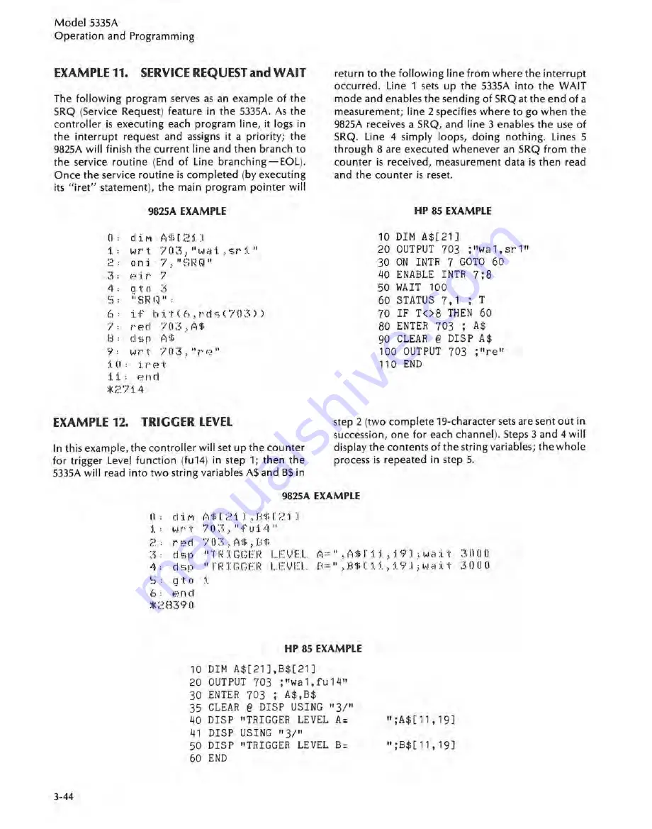
Page 77: ...ables the sending of SRQ at the end of a measurement line 2 specifies where to go when the 9825A receives a SRQ and line 3 enables the use of SRQ Line 4 simply loops doing nothing Lines 5 through 8 are executed whenever an SRQ from the counter is received measurement data is then read and the counter is reset HP 85 EXAMPLE 10 DIM A 21J 20 OUTPUT 703 wal srl 30 ON INTR 7 GOTO 60 40 ENABLE INTR 7 8 ...

Page 78: ... are set to V V 0 2V The resultant Time Interval measurement is read into A and displayed as T I See The value of V ischanged to 0 9 V 7 V After a two second wait the string command is sent again with the new value for V programmed into both channel trigger levels The second measurement is read into A and displayed After a two second wait the program loops to the beginning and starts again 9825A E...

Page 79: ...haracteristics 3 238 C Channel Option 030 3 239 Option 030provides a C Channel Input Module which expands the frequency counting range of the counter to 1 3 GHz A front panel control adjusts the input sensitivity A front panel preamp power recep tacle is provided Refer to Specifications Table 1 1 for the specific operating characteristics 3 240 Programmable Input Option 040 3 241 The programmable ...

Page 80: ... a DISPLAY CHECK and a FRONT PANEL CHECK The operator should perform both tests Model 5335A Operation and Programming a DISPLAY CHECK To perform the HP 5335A DISPLAY CHECK mo mentarily press the key labeled CHECK Verify that all display annunciators except STBY and the A and B Channel Trigger lights cycle ON and OFF Pressing any Function keywill return normal operation b FRONT PANEL CHECK To perfo...

Page 81: ...L EASUAEMEHTS EXCEPT GATE t lME AMOTftGLVt iMA e MODIFIED 8Y OFFSETING NORMALIZING 4NO SCALING MEASUREMENT OFFSET NORMU DISPlAY CALE NUM8ER ENTRY ENTER VALUES INTO THe OFFSET HOI MU OI SeAl Rr lIST l RS BY USING THE SHIFTED BLue LABELEO KEVS PRESSING ANY OF THE THREE BLUE GVS sr II t Uf I Iil Et TIIY TN T MY S LAMP WILL FLASH AND THE DISPLA V WILL SHOW TNE ClliW IfT Ll IIi III fWAt lI GI8T 11 ENTE...

Page 82: ... Error Incorrect Command 1 1 HP IB Error Numberoutofrangeorincorrect number within command 7 0 Check Error Cable may not be connected between T B O and INPUT A for extended CHECK Diagnostic 01 or Diagnostic 14 Table 4 2 Fail Messages FAIL 1 0 1 4 ROM FAILURE U22 1 5 1 8 ROM FAILURE U23 1 9 ROM FAILURE SPECIALS 2 0 RAM FAILURE 6802 2 1 RAM FAILURE U26 2 2 RAM FAILURE U25 3 1 OUT BUS PROBLEM BIT 5 O...

Page 83: ...in the counter s circuitry After the power up sequence the counter will initialize itself All Math and Statistics will be OFF the function will be FREQ A and the Gate and Cycle Modes will be in NORM All of the input controls will be set according to their switch positions If Option 040 is installed the input switches LED will be in the OFF condition 4 17 Any failures during the power up cycle will...

Page 84: ...5 000 00 V 3 00000 V 5 20000 V NOTE If TIME BASE OUT is not connected to INPUT A ERROR 7 0 will be displayed r Model 5335A Performance Tests 4 22 Front End Input Amplifier Switch Test Procedure III 4 23 Perform the following steps to test the Input Amplifier switches a Set 5335A front end INPUT switches asfollows CHANNEL A B SLOPES NEGATIVE IN PRESETS OFF ATTEN X10 IN COM A ON IN AUTO TRIG ON IN b...

Page 85: ...335A display shows 8 8 8 only the 4th 6th and 8th digit ON e Verify and record on test card f Set 5335A rear panel EXTERNALARM START and STOP slope switches BOTH to Negative DOWN 4 4 g Observe 5335A display shows 8 8 8 only the 4th 5th and 7th digit ON h Verify and record on test card i Remove Signal from TIMEBASE IN j Observe 5335A display 4th digit goes blank k Set 5335A rear panel EXTERNALARM S...

Page 86: ...il the lower right key is pressed NOTE INPUT section if for Option 040 only c Observe as each key is pressed 1 The 0 EXPONENT will light and two digits on the display will match digits in Figure 4 3 2 The key s lamp will turn ON except for RESET CHECK and CYCLE NORM which have no lamp d Verify and record on test card NOTE You must cycle Power Switch to STBY and back to ON to exit the KEYBOARD CHEC...

Page 87: ...ency of the HP 8660C d Observe the 5335A display shows the output frequencies of the HP 8660C within the C Channel published Specs e Verify and record on test card 4 32 Programmable Input Amplifier Test Option 040 Procedure VIII 4 33 Perform the following steps to use the Option 040 INPUT test a Connect the 5335A Trigger Levels OUT A B rear panel to the 1740A oscilloscope as shown in Figure 4 4 b ...

Page 88: ...ockwise position Model 5335A Performance Tests b Set the 5335A power switch to STBY then to ON Verify that 1 Red LED STBY lamp is OFF 2 All display and annunciator lamps turn ON momentarily excluding STBY and trigger lamps 3 Display shows the selected HP IB address 4 FREQ A and Hz lamps are ON display shows 0 5 All other lamps are OFF except Trigger lamps which may be on 6 Fan is ON e Record resul...

Page 89: ...to Figure 4 5 The selected key LED will remain ON while the number is being played A 0 will be displayed in the exponent section of the display during the test 4 45 Perform the following stepsto useKEYBOARDtest a Press SCALE 1 7 ENTER Display shows dIAG 17 4 48 Perform the following steps to use the EXTERNAL ARM switch test a Set the HP 5335A power switch to STBY then ON Usean HP 3325A Synthesizer...

Page 90: ...nd the gate time is varied throughout its range The 5335A should display the correct count 4 52 Perform the following stepsto use the GATETIME test a Set the 5335A power switch to STBY then ON b Set the 5335A front panel controls as follows GATE MODE NORM CYCLE NORM FUNCTION GATE TIME GATE ADJ fully ccw c Vary the GATEADJ control from full ccw to full cw position the 5335A should display from less...

Page 91: ...00 switch to 1 MO set the AC DC switch to ac coupling Set the 3325A through a 500 feedthrough to the 5335A INPUT A Set the 3325A to output a 30 Hz sine wave at 25 mV rms Increase the frequency of the 3325A and verify that the 5335A displays the proper frequency from 30 Hz to 20 MHz g Measure actual sensitivity by decreasing the 3325A level until the 5335A gives an unstable count at these frequenci...

Page 92: ...335A Channel B minimum signal sensitivity level The frequency is slowly increased from dc up to 20 MHz at constant level and the 5335A readi ng is checked for the proper count For the range of 20 MHz to 100 MHz a different generator is used 4 61 Perform the following steps to use the B Frequency Response Test a Press SCALE SMOOTH 1 7 ENTER This will enable special function Frequency B DC to 20 MHz...

Page 93: ... 332SAlevel until the 5335A gives an unstable count at these frequencies 200kHz 500kHz 1 MHz 10 MHz 20 MHz k Record results on test card VALUE 20 MHz to 100 MHz de coupled I Connect the HP 8654A Signal Generator to the 5335A INPUT B as shown in Figure 4 10 m Set Channel B AC OC switch to de coupling Set the 8654A to output a 20 MHz sine wave at 25 mV rms Increase the frequency of the 8654A and ver...

Page 94: ...ts INPUT Channel A and B 1 MOJ50n son ON Trigger Level PRESET X10 X1 ATTN X1 OUT OFF AC DC DC OUT OFF FILTER Option 040 OFF AUTO TRIG OUT OFF COM A IN ON o to 20 MHz b Connect the 3325A Synthesizer Function Gen erator to the 5335A INPUT A as shown in Figure 4 11 c Set HP 3325A to 10 Hz 10 kHz S MHz and 20 MHz at 25 mV rms sine wave The 5335A should display a stable ratio as shown HP 3325A HP 5335A...

Page 95: ... front panel controls as follows FUNCTION TIME A B MATH Off LEDs off STATISTICS Off LEDs off GATE MODE MIN LED ON CyCLE NORM GATE AD fully ccw INPUT Channel A and B 1 Mn SOn son ON Trigger Level PRESET X10 X1 ATTN X1 OUT OFF AC DC DC OUT OFF Channel A Slope pas OUT OFF Channel B Slope NEG IN ON FILTER Option 040 OFF AUTO TRIG OUT OFF COM A IN ON I REFERENCE IN TIME BASE OUT r r r t l r l fili o 0 ...

Page 96: ...F Slope POS OUT OFF Trigger Level PRESET FILTER Option 040 OFF AUTO TRIG IN ON COM A OUT OFF c Using the HP 1743A oscilloscope Delta Time function set HP 8082A to output a W 4 microsecond pulse with a period of 10J lS at the fastesttransition times approximately 1 ns The 5335A should display 4 000J ls 5 ns d Record results on test card PASS FAIL e Set the 5335A channel A slope to NEG IN ON Verify ...

Page 97: ...s FUNCTION RISE FALLA MATH Off LEDsoff STATISTICS Off LEDsoff CyCLE NORM INPUT Channel A and B 1 MD 50D SOD ON X10 X1 AnN X1 OUT OFF AC DC DC OUT OFF Channel A Slope POS OUT OFF FILTER Option 040 OFF e Using the HP 1743A oscilloscope Delta Time function set HP 8082A to output a pulse as shown in Figure 4 16 Verify that the 5335A displays 400 ns 82 ns d Set the 5335A for the FALL TIME A function by...

Page 98: ...Hold OFF b 0 to 360 Range Hold ON c Frequency Range 30 Hz to 1 MHz 4 84 DESCRIPTION A Pulse Generator with com plementary outputs drives both channels A and B of the 5335A under test The counter is set to the PHASE A rei B function and the channels are set in SEP mode The 5335A should display the phase relation ship between the two signals 4 85 Perform the following steps to use the PHASE A rei B ...

Page 99: ...epeat for 4 0000 volts h Record results on test card PASS FAIL i Set DC Standard for 40 000 volts The counter should display 40 00V 38 mV Repeat for 40 000 volts j Record results on test card PASS FAIL k SET DC Standard for 400 00 volts The 5335A should display 400 0V 380 mV Repeat for 400 00 volts I Record results on test card PASS FAIL 4 90 Channel C Option 030 TestProcedure XIV 4 91 SPECIFICATI...

Page 100: ...ing a 1 dBm reading on the power meter and verify that the 5335A displays the proper frequency from 1 GHz to 1 3 GHz h Measure actual sensitivity by decreasing the 86603A level until the 5335A gives an unstable display at these frequencies 1 1 GHz 1 3 GHz i Record results on test card VALUE REAR TIME BASE OUT 86603A 8660C 86603A SYNTHESIZED SIGNAL GENERATOR 436A POWER METER INPUT 1250 0780 OUTPUT ...

Page 101: ...ator if the test has been successfully completed At the conclusion of each test the program stops and displays the current check point To advance to the next test simply press CONTINUE If it is desired to repeat a test key in cont and the check point number and press EXECUTE e g to repeat test 3 key in cont 3 To go on to the next test after looping press CONTINUE 4 100 At the end of the HP IB Veri...

Page 102: ...4 into the 9825A or insert cassette HP PIN 59300 10001 revision L or later d Load and run file 0 key in Idp0 press EXECUTE e Key in the model number of the instrument to be tested i e 5335 press CONTINUE f Key in select code 728 press CONTINUE g Set up the 5335A as described in the printout and press CONTINUE h Always pressCONTINUE to advancethe program Table 4 3 9825A Verification Program Prinout...

Page 103: ...t i j r i n t j c n F f E C C1 J n d H2 G n 1 un v ii J n j j Checks the 5335A power up conditions and performs basic Frequency A measurement 4 22 l j T i J L 1 1 Set the 5335A in the REMOTE and LISTEN state Scanned by KN5U Reproduced with permission Courtesy of Agilent Technologies Inc ...

Page 104: ... the 5335A to make a FREQ A measure ment and to output the data 1C r p C j F e t l r J c c 1 C H E C r j 1 G I C c n d I Operator verification of proper operation of the front panel LOC REM function No remote codes sent 4 23 Scanned by KN5U Reproduced with permission Courtesy of Agilent Technologies Inc ...

Page 105: ... 1 r Programs the 5335A to go to remote and activates counters local lockout LLO 4 24 The 5335A is programmed to wait until it is addressed to talk before making another measurement At the end of the measurements the program will beep Scanned by KN5U Reproduced with permission Courtesy of Agilent Technologies Inc ...

Page 106: ... 1 T E l n f 1 J w v l i 1 The 5335A is first programmed for a particular setting then the counter will teach the 9825A the front panel setup When CONTINUE is pressed the 5335 is set up for a Period A measurement i When CONTINUE is pressed again the 5335A will learn from the 9825A 4 25 Scanned by KN5U Reproduced with permission Courtesy of Agilent Technologies Inc ...

Page 107: ... l I j 1 t j _ _ t 0 The 5335A is set up and programmed for a Frequency B measurement 4 26 r i r _ t T r r v 1 L u h i i ir i J _ t ii G 1 The 5335A is set up to measure and display Channel A and B trigger levels Scanned by KN5U Reproduced with permission Courtesy of Agilent Technologies Inc ...

Page 108: ... Verification Program Printout Continued iT j i M J 1 j l i J 1_ _ N I 1 j ci if C iCl i t t C u t 1 i e d is 1 Both gate time ranges of the 5335A are programmed 4 27 Scanned by KN5U Reproduced with permission Courtesy of Agilent Technologies Inc ...

Page 109: ... Performance Tests Table 4 3 9825A Verification Program Printout Continued The 5335A is exercised in the Rise and Fall Time mode 4 28 Scanned by KN5U Reproduced with permission Courtesy of Agilent Technologies Inc ...

Page 110: ... Tests Table 4 3 9825A Verification Program Printout Continued L CHECK POINT 12 exercises the gate open and gate closed functions 0 C i G 1 4 29 Scanned by KN5U Reproduced with permission Courtesy of Agilent Technologies Inc ...

Page 111: ...C 1 1 G f T E I 0 f j l G I F C 1 E C T E i F E T I rl 1E I f T E H L M L c If O j C H T E 1 G f f H G 1 d E t 1 i 1 l L G f i i The 5335A is programmed in the TIME A B function 4 30 The INVERSE TIME A B is exercised the actual dis played value may differ Scanned by KN5U Reproduced with permission Courtesy of Agilent Technologies Inc ...

Page 112: ...ondins to FIGUFE H Programs the 5335A for Diagnostic 17 Figure A MATH FUNCTION 09 13 17 21 25 03 053 STATISTICS INPUT 10 14 18 22 26 35 37 39 41 43 45 02 04 06 08 11 15 19 23 27 GATE MODE 36 38 40 42 44 46 29 31 33 12 16 20 24 28 GCYCLE 30 32 3 4 31 Scanned by KN5U Reproduced with permission Courtesy of Agilent Technologies Inc ...

Page 113: ... i n c L G t c e c n d lh2n 53358 011_ r 1 1 j j C1 1 i 1 The 5335A is programmed to fully testthe front end by connecting the Time Base Out to INPUT A 4 32 The 5335A is set up to verify the proper operation of the DVM Option 020 Scanned by KN5U Reproduced with permission Courtesy of Agilent Technologies Inc ...

Page 114: ... j T i C F T I Ci r l i 1 C e t o i l i t c l i G e o c t i i t d l 0 c t i G t d Programs and verifies the correct operation of the Channel C Option 030 Exercises Option 040 Front End Input momentary switches IPerforms a functional test on the 5335A Channel A and B DACS 4 33 Scanned by KN5U Reproduced with permission Courtesy of Agilent Technologies Inc ...

Page 115: ... Lv i 23 prt runtion F8 Q A and Hz annun 24 or t lamPE are ON Then 5335A will display 25 or t lOt DOC COO 6 with Hz LED ONi GATE A 26 o r t ano B Trigger lites f La s h i nq c v r s pc 2 27 C1Sf A l 11 1 A l6 istD 28 if X liato rot 29 2 z d s p AS l Jl 2 30 or t D iwrt 16 A l 13 31 ort Program 8enc1s 5J3SA listen accref s spc 32 pr t Verify Display is sarne as ahove Excect LIS PEl and 33 prt REMOT...

Page 116: ...f x Lr ci t c rot 83 7 dsp 11 1 11 7 84 nr t D iwrt 16 A I 13 7 8 r r t TEACH LEARN est ispC 86 rrt Verify that the 5335J displays l1 224 49 15 Hz ispe 2 87 rsp F Etp 8 8 r e IT s i i IV r t s j f uLrn s 1 12 2 4 4 8 8 0 0 89 r r t 5335A will teach the 98251 the front panel setup spc 2 90 VJ r t s j DC 91 for 1 1 tc 30 92 rdt sj A I next I 93 ato 1 if 11 24 17 and A 25 34igto 1 94 tc 2iif A 26 68 ...

Page 117: ...sEconds spe 2 137 wrt sj fu13gwlrhO jred sj B 138 d sp A l 11 lO A l6 jste 139 if X l gto r p t 140 11 prt D rt 16 1 13 ll idf P A l ll 11 141 r rt RISE FALL TIf 1E Test spc 142 p r t SETUP Corneet TEO from rear panel to INPU T A spe 2 143 dst E stf 144 dsp A l ll I iprt RISE TIME test 14S prt VEPIFY RISE FAIL A lamp is or 146 rt S33SA isplays approximately 30 nanoseconds 147 prt Gate Mode MIN law...

Page 118: ...14 1 rt D wrt 16 A l 13 14 crt FRONT PANEL Switch Test spc pr t Press each mome nt ar y type prt key on the 533SA front panel beginning with crt upper left key MJ TH DISABLE prt and gc down each co1uIT n spc 2 prt E dsp See FIGURE A spc 2 stp rt sj fu99ms17 wait 100 lcl sj prt A nUIT ber will be displayed when crt a key is cressed corresponding to nr t FIGUFE A Spc 2 dsop A l ll 14 A 16 stp if X l...

Page 119: ...rt tary switches are activat ed d e ac t Lv a t ed s v r s pc 2idsp E istp wrt sj inaflasl iw it Diwrt sj az1aal wait D wrt sj axl iwait Di rt sj bx1 iwait D wrt sj bzlba1 iwait Diwrt sj bf1bsl iwait D wrt sj co1a 111 iwait Diwrt sj coOauO iwait D wrt sj bfObsO iwait Diwrt sj bzObaO iwait Diwrt sj bxO iwait D wrt sj axO iwait u rwr t sj azOaaO iwait Dj w r t sj intrlatObtO prt DAC Test isr c 2i 15...

Page 120: ...ance Tests 282 ato 14 283 gto 15 284 gto 16 285 gto 17 286 gto 18 287 end prt C spc prt END OF 5335A HP IB TEST 288 beepiwait 500ibeepispc ort C iSPC 6 289 wrt sj in lc1 sj sp END OF 5335A HP IB TEST 290 end 24 989 4 39 Scanned by KN5U Reproduced with permission Courtesy of Agilent Technologies Inc ...

Page 121: ... At the end of the HP IB Verification Program the controller will ask if you want to repeat one of the tests Enter the appropriate nu mber for the test needed asindicated on the controller display then press END LINE the selected test will then be repeated Enter 13 if you wish to terminate the test program At the end of the particular test the question of whether you wish to repeat a test is asked...

Page 122: ...3 1 5335A POWER UP CHECK DISP 430 DISP Turn 5335A power OFF then ON VERIFY 470 DISP RED LED STBY lamp is OFF 490 DISP All lamps turn ON momentarily 510 DISP Selected HP IB add displayed 530 DISP FREQ A Hz lamps are ON 550 DISP Display shows 10 000 000 6 570 DISP with Hz LED ON GATE A 590 DISP Trigger light flashing DISP DISP USING K A 16 595 PAUSE 610 IF X O THEN 6210 630 CLEAR DISP C GOSUB 6410 D...

Page 123: ...ify that the 5335A disp1ays ll 224 49 15 Hz 1690 DISP USING 2 OUTPUT S USING I K pb 1710 FOR 1 1 TO 30 OUTPUT S USING I B A I NEXT I LOCAL S 1730 DISP A 16 BEEP PAUSE 1750 IF X O THEN 6210 1770 CLEAR DISP C GOSUB 6410 DISP 1790 DISP A 1 12 6 FREQUENCY B mode TEST DISP 1810 DISP SETUP Connect Time Base Out TBO 1830 DISP from rear panel to INPUT B DISP USING 2 1850 DISP E PAUSE 1870 OUTPUT S coOfu17...

Page 124: ...SP A 1 12 10 OVERFLOW mode TEST DISP 3050 DISP Verify that the ONLY lamps lit during the 11 second wait 3070 DISP period are 3090 DISP Hz GATE LISTEN 3110 DISP REMOTE FREQ A Manual GATE MODE and 3130 DISP A trigger lamp flashing 3150 DISP 5335A Displays 0 DISP USING 2 DISP USING I K E 3155 PAUSE 3170 OUTPUT S inwalgm3 DISP A l lO 10 A 16 WAIT 11000 3190 OUTPUT S gc ENTER S B BEEP CLEAR DISP 3210 D...

Page 125: ... OUTPUT S fu99msO DISP DISP USING I K A 16 PAUSE 4295 OUTPUT S in 4310 IF X O THEN 6210 4330 CLEAR DISP C GOSUB 6410 DISP A O 4350 DISP If DVM Option is installed enter 1 if not enter 0 then 4355 DISP press END LINE DISP INPUT A 4370 IF A O AND A l THEN 4330 4390 IF A O THEN 4790 4420 CLEAR DISP C GOSUB 6410 DISP OUTPUT S in LOCAL S 4430 DISP A 1 12 14 OPTION 020 DVM TEST DISP 4450 DISP SETUP a Co...

Page 126: ...UTPUT S axl WAIT 0 5330 OUTPUT S bxl WAIT 0 5350 OUTPUT S bzlbal WAIT 0 5370 OUTPUT S bflbsl WAIT 0 5390 OUTPUT S colaul WAIT 0 5410 OUTPUT S coOauO WAIT 0 5430 OUTPUT S bfObsO WAIT 0 5450 OUTPUT S bzObaO WAIT 0 5470 OUTPUT S bxO WAIT 0 5490 OUTPUT S axO WAIT 0 5510 OUTPUT S azOaaO WAIT 0 5530 OUTPUT S intrlatObtO 5550 CLEAR OISP C OISP 5570 OISP A 1 12 16 OPT 040 PROGRAMMABLE INPUT TEST OISP 5590...

Page 127: ... DISP If you need to repeat a Check Point enter the Check Point 6217 DISP number 1 thru 16 if not 6220 DISP enter 0 then press END LINE DISP INPUT X 6230 IF X O OR X 16 THEN 6210 ELSE OUTPUT S waO 6250 IF X O THEN 6330 6295 IF X 12 THEN 6315 6310 ON X GOTO 390 630 750 870 1230 1770 2090 2270 2570 3010 3350 3730 6315 ON X 12 GOTO 4150 4330 4790 5090 6330 CLEAR DISP USING 4 DISP C DISP 6350 DISP END...

Page 128: ...P NO PASS FAIL I POWER UP SELF TEST II SUPERCHECK III KEYBOARD CHECK IV REAR PANEL EXTERNAL ARM SWITCH TEST V KEYBOARD CHECK VI DVM TEST Option 020 VII CHANNEL C TEST Option 030 VIII PROGRAMMABLE INPUT TEST Option 040 OPERATION VERIFICATION RECORD TEST CARD 4 47 Scanned by KN5U Reproduced with permission Courtesy of Agilent Technologies Inc ...

Page 129: ...ATE TIME 20 ms to 4 s 100 us to 20 ms VI FREQUENCY RESPONSE and SENSITIVITY Channel A 25 mV rms A DC to 20 MHz de coupled 0 01 Hz 10 Hz 100 kHz 10 MHz 20 MHz B 30 Hz 20 MHz ac coupled 30 Hz 10 kHz 1 MHz 10 MHz 20 MHz C 200 kHz 20 MHz SOn 200 kHz 500 kHz 1 MHz 10 MHz 20 MHz D 20 MHz 200 MHz de coupled 20 MHz 50 MHz 125 MHz 200 MHz E 20 MHz 200 MHz ac coupled 20 MHz 50 MHz 125 MHz 200 MHz 4 49 Scann...

Page 130: ...oupled 20 MHz 50 MHz 100 MHz VII RATIO AlB Display 1 cou nt 10 Hz 1 10 kHz 1 00 5 MHz 1 0000 20 MHz 1 000 00 50 MHz 2 50000 100 MHz 5 00000 150 MHz 7 50000 200 MHz 10 000 00 VIII TIME INTERVAL AND INVERSE TIME INTERVAL Time Interval 100 5 ns Inverse Time Interval 10 0 0 5 10 6 units s IX PULSE WIDTH A AND PULSE WIDTH B Pulse Width A Positive Pulse 4 000 us 5 ns Negative Pulse 6 000 us 5 ns Pulse W...

Page 131: ... XI SLEW RATE A 2 00 0 65 Vis XII PHASE A rei B 1BO 1 5 degrees XIII DVM TEST Option 020 Shorted input OV 600 mY 4 000V 3 8 mV 40 00Y 38 mV 400 0V 3BO mV XIV CHANNEL C TEST Option 030 A 150 MHz to 1 GHz s 27 dBm 150 MHz 500 MHz BOOMHz 1 0 GHz B 1 GHz to 1 3 GHz s 7 dBm 1 1 GHz 1 3 GHz 4 51 Scanned by KN5U Reproduced with permission Courtesy of Agilent Technologies Inc ...

Page 132: ... PERSONNEL WHO ARE AWARE OF THE HAZARDS INVOLVED FOR EXAMPLE FIRE AND ELECTRICAL SHOCK WHERE MAIN TENANCE CAN BE PERFORMED WITHOUT POWER APPLIED THE POWER SHOULD BE REMOVED BEFORE ANY REPAIR IS COMPLETED EN SURE THAT ALL SAFETY FEATURES ARE INTACT AND FUNCTIONING AND THAT ALL NECESSARY PARTS ARE CONNECTED TO THEIR PROTECTIVE GROUNDING MEANS 5 10 ADJUSTMENT PROCEDURES 5 11 A1 Power Supply Adjustmen...

Page 133: ...TOP VIEW SEE TOP VIEW 1740A OSCILLOSCOPE 100 MHz CHANNEL B INPUT 3312A FUNCTION GENERATOR I OOOO ODD DODD o DODD ODD DODD 000 000000000 00 V PEAK TO PEAK INPUT A CHANNEL A I2l INPUT Figure 5 1 Input Amplifier Adjustment Setup 5 2 Scanned by KN5U Reproduced with permission Courtesy of Agilent Technologies Inc ...

Page 134: ...r the Channel A adjustment connect the oscilloscope A channel probe to the junction of A2U11 7 and A2R39 Model 5335A Adjustments I WARNING l DO NOT SHORT THE PROBE TO ANY OTHER TRACES OR COMPONENTS OR DAMAGE WILL OCCUR TO THE CIR CUITRY PARTICULARLY TO THE AMPLI FIER SCHMITT IC S e Set the oscilloscope for the X V mode and calibrate by centering the dot at center screen f Position both A3R96 offse...

Page 135: ...dard to 4 000volts then turn the DC Standard and the 5335Aoff disconnect all test equipment 5 4 5 17 A9 Channel C Option 030 Adjustment Procedure 5 18 To perform the adjustments required for the CHANNEL C proceed as follows a Turn on 5335A and allow instrument and CHANNEL C to warm up for 5 minutes b Remove the instrument top cover and locate variable resistors R22 L R23 H and R24 K on the A9 Chan...

Page 136: ... dBm 10 0 mV 26 99 dBm Figure 5 3 Channel C Sensitivity Adjustment Setup 436A POWER METER OUTPUT 1250 0780 ADAPTER 1 N TO BNC o A 5011 BNC CABLE N TO BNC 11667A A POWER SPLITTER _ _ _ _ _ 8660C 86603A SYNTHESIZED SIGNAL GENERATOR I I U 8481A POWER SENSOR INPUT 5 19 Oscillator Adjustment Procedure Local and Option 010 5 20 Every few months the oscillator should be checked to a house standard When a...

Page 137: ... BASE IN as shown in Figure 5 5 c Set the 5335A front panel controls as follows FUNCTION PER A GATE MODE NORM CyCLE NORM INPUT Channels A and B SLOPE negative 1 MDJ50n son IN TRIGGER LEVEL PRESET OUT X1 X10 ATTN X1 OUT AC DC DC COM A OUT AUTO TRIG OUT d Set the 8640B to output a 110 MHz signal at 15 mV rms NOTE 8640B amplitude may be increased up to 20 mV rms if necessary to obtain stable count wi...

Page 138: ...ctor Adjustment c Connect a Function Generator HP 3312A to Input A set the function generator to output a 2OOJ s quare wa e at 581hflV p p 30 HiSINE WAIlr AI 5VP f d Connect the DVM HP 3455A positive input to either side of A3R54 422ohms and the DVM negative input to the ground test pin on A3 e Adjust A3R100 PK so that the DVM dis plays m j Z 44 V f 07rtV f Rotate Channel A Trigger Level Pot to th...

Page 139: ...AL ARM IN connector through a 500 feed through as shown in Figure 5 6 d Set the HP 3325A to output a 3 volt peak to peak square wave with an offset of 1 5 volt at a frequency of 100 Hz e Set the 5335A EXTERNAL ARM AD through the rear panel to full clockwise position This will set the External Arming circuitry for TTL level signals f Observe that the 5335A displays about 10 ms Also the 1740A displa...

Page 140: ...t panel controls as follows Pe NER Hlly tii 1 6N c Set the 3312A Function Generator to output a 1 0 kHz sine wave at 100 mV p p Model 5335A Adjustments d Connect the test equipment asshown in Figure 5 7 for the Channel A adjustment connect the oscilloscope Channel A probe to the junction of A11R47 and R54 I WARNING I DO NOT SHORT THE PROBE TO ANY OTHER TRACES OR COMPONENTS OR DAMAGE WILL OCCUR TO ...

Page 141: ...TOP VIEW SEE TOP VIEW 3312A FUNCTION GENERATOR Ir ooO DODD I DDDD DODD ODD D DDD O ODD 1740A OSCILLOSCOPE 100 MHz V PEAK TO PEAK INPUT A 00000 CHANNEL A INPUT c J CHANNEL B INPUT Figure 5 7 Programmable Input Amplifier Adjustment Setup 5 10 Scanned by KN5U Reproduced with permission Courtesy of Agilent Technologies Inc ...

Page 142: ...a Jaa 1046 S Uil J o aV at SO re P fh 30 I ll SINe IJJPrvt CHANNEL A 4r 5V P f e Connect the HP 3455A DVM positive input to A11 ATL test point and the DVM negative input to the GAA test point Model S335A Adjustments 2 f Adjust A12 PK so that DVM displays 24e IiPI IS mV 2 44v J01l1V g Rotate Channel A Trigger Level Pot to the CW position adjust 1 PK so that DVM displays jqJIO mv 5 tm IIJJ 2 4 V 0 7...

Page 143: ...0 X1 ATTN X1 OFF AC DC DC OFF FILTER OFF d Set the 3312A Function Generator to output a 50 Hz squarewave at 5 volts p p Make a note of the measure ment value displayed by the 5335A e Set the 5335A Channel A ATTENUATOR TO X10 f Locate variable capacitor A12 C46 g Adjust A12 C46 so that the 5335A display is the same as the value noted in step d 0 3 nanoseconds 5 34 A12C30 Adjustment Procedure a Swit...

Page 144: ... on Change the 8654A output range to the 300mV scale 10 times output level of step e Increase the output level until the 5335A displays a stable count of 100 MHz Record this signal level as CHAN A X10 xxx mV and save for step IIgll g Divide the value of recorded level from step IIf by recorded level from step lie to determine the actual atten uation factor of CHAN A Result should be approximately ...

Page 145: ...ust A12 C30 so that the 5335A display just gives a stable count of 100 MHz 2336 Paragraph 5 32 step a Change Part Number of A12 Programmable Input Amplifier Assembly from 05335 60012 to 05335 60032 Page 5 13 Adjustments All Serials Paragraph 5 36 step a Add R48 A and R53 B to the list of variable resistors in step a Paragraph 5 36 step b Delete the first sentence Repeat step 5 32 e and replace wit...

Page 146: ...sine wave at a minimum output level on the 30mV range lncrea the output level of the 8654A until the 5335A aysa stable count of 100 MHz Record this e e Set the 5335A Channe Attenuator to Xl0 ON and COM A mo ary switch to ON Set the 8654A output ra 0 the 300 mV scale Se e 8654A to output a level 10 times the ously recorded level in step d Adjustment Procedure 5A line power from ON to OFF b Press SC...

Page 147: ...ys 5 12 1 mV ALL L i I El S ffIIZE IHOIl 1L 4 NT 3 Afl Au rU S E f PrCl TLj AS A2 uvo jt IP IZE7 1 On A2 lu5 ANY Z plp 0 A v ru sJW P LItiet Stllf ZJe Sl5T1J1t FOL L 71fe fZoc Lrz Lt f It P A 5 1 f 6 rLt l I 1f1 h fl 53 t o l l lt4 v l4 FOfL Lt 5 e Disconnect DVM positive terminal from BTL test point and connect the terminal to ATL test point also connect DVM negative terminal to GAA Vary R75 5 12...

Page 148: ...er check digit CD e The total quantity Qty used in the assembly d The description of the part e A typical manufacturer of the part in afive digit code f The manufacturer s number for the part 6 8 The total quantity of each part used within an assembly is given only once at the first appearance of the part number in the list 6 9 ORDERING INFORMATION 6 10 To order a part listed in the replaceable pa...

Page 149: ...COMP composition in parts list PL phase lock V F volts filtered COMPL complete log logarithm ic PLO phase lock oscillator VFO variable frequency oscillator CONN connector LPF low pass filter PM phase modulation VHF very high frequency CP cadmium plate LV low voltage PNP positive negative positive Vpk volts peak CRT cathode ray tube m metre distance P O part of Vp p volts peak to peak CTL complemen...

Page 150: ... 75 1IlZ50VDC AL CAPACITOR FXD 017F 75 1DZ 20VDC AL CAPACITOR FXD 11 1F 20 51lVDC CER CAPACITOR FXD 8DOOUF 7S IUZ 30VDC AL 2 DIODE ZNR lN534UB 6V 5 7 PD 5W II 1UA DI0DE ZNR lN5354B 17V 51 PD 5W TC 75Z DIODE ZNR IN5340B 6V 51 PD 5W IR IUA DIODE PWR RECT 100V 6A NOT ASSIGNED 2 DIODE PWR RECT 41l0V lA DIODE SWITCHING BOV 200MA 2NS DO 35 DIODE FW BRDG 200V 2A DIODE PWR RECT 10DV 5A 5US DIODE PWR REeT ...

Page 151: ...0 0269 A1XF2 2110 0269 0 FUSEHOI_DER CUP TYP E 25D FUSE 28480 2110 0269 AIXF3 2110 0269 0 FUSEHOl DER CLI P TYPE 25D FUSE 213490 2110 0269 A lXF4 2110 0269 0 FUSEHOI_DER CI IP TYPE 25D FUSE 2a480 2110 0269 AIXKI 0490 0468 3 1 SOCKET RL Y 16 CONT CRADL E DIP SLDR 28480 0490 0468 AI MISCI LLANEOLIS PARTS A1MP1 05335 000fl5 5 1 HEAT SINK FOR A1CR11 28480 O 335 00005 See introduction to this section f...

Page 152: ...20 40 VK OO 20 48 VI 200 20 411 VK OO 20 48 SPS 233 C4 1 8 TO IOOI F C4 1 8 TO I 00 I F C4 1 8 T 0 11 0 F 06 8 694 3 06 13 694 li C4 1 8 TO 16 F 06 8 6 4 5 1 4 l B TO Illli F C4 1I1 I TO IIO F C4 1I8 TII I IIO F C4 1 8 T 0 162 F C4 1 8 TO 40G _ F C4 1 B TO 4002 F C4 1 8 TII 16 2 F C4 1 8 TO 511 R F 0698 6943 C4 1 8 TO 4002 F C4 I B TO 4C02 F C4 1 8 TII 400 F C4 1 8 TO 4002 F C4 1 8 T 101l F C4 1 8...

Page 153: ...546 24546 24546 01121 24546 4546 24546 28480 28480 27014 06665 27014 06665 0661 5 3L585 04713 04713 15818 06665 04 713 Ol 95 7014 01 1 95 fl1295 o 129 1 B4IlD D4Un IJ48 0 B4E10 C3 1 8 TO IOOR F C3 1 18 TO 261 R F C3 1 18 TO 383R F C4 1 8 TO 82R5 F 206M71 C4 l B TO I002 F C4 1 8 TO 133il F C4 I S TO 82R5 F C4 1IB TO l 003 F 06tlS 8094 o 698 b S69 C4 1 8 TIl 75RO F C4 1I8 TII 301 F C4 118 T 11 0 l F...

Page 154: ...FXIl OIUF 20 100VDC eER 28480 0160 3879 A3C32 0160 3879 7 CAPAClTOR FXD OllJF 20 100VDC CER 213480 0160 3B79 A lC33 11160 3079 7 CAPAC nOR XD 111111 20 100VIlC CER 8480 11160 3879 A lC34 0160 47113 8 CAPACITOR FXD 68PF i 5110VDC CER 11 11 U480 Dl60 4703 A lC35 0160 41140 6 CAPACITOR FXD 1000PF 5 100VDC CEI 20480 0160 4040 A3C36 0160 3879 7 CAPACITDR FXD OIUF 20 100VIlC CER 28480 0160 31379 A 3C37 ...

Page 155: ...INDUCTOIl INDUCTOR 1 1480 D4IJO 1l4E10 n400 2Fl4BO 2n480 2B480 2 8480 20480 28480 20480 21 41l0 2B4HO 21l4BO 8480 28480 28480 28480 28480 28480 28480 2B4BO 28400 8480 2H4no in480 20400 8480 8400 1l480 28480 28480 28480 28480 28480 1 4BO D400 4546 4 4f 1 t 4 54b 4546 284 80 2B4BO 24546 24 546 24546 24546 24546 24546 24 46 B48n 04011 4 546 2D4BfI 4 j46 24546 24546 2134130 24546 24546 28480 05 8 003 ...

Page 156: ...6 7 RESISTOR 511 i x 125W F TC O IOO 0 98 7222 I RESISTOR 261 17 051 4 F TC O IOO 0699 0073 8 RESISTOR 10M t x 1 5W F TC O 150 0698 6400 RESISTOR 900K 1 25101 F TC 0 100 0698 3922 0 RESISTOR 487K 1 1 125W F TC 0 50 0698 3922 0 RESISTOR 487K n 1 5W F TC 0 50 0698 7227 6 RESISTOR 422 I r O JWF TC O 1 00 0698 7212 9 RESISTOR 100 1 05W F TC O IOO 2100 3802 2 RESISTOR liAR W SW 10K 20 UN SPST NO 0698 7...

Page 157: ...CH PB DrDT ALTNG 25A 115VAC 2841 10 3101 2498 A3LJl 1326 0600 9 2 IC OP AMP LOW BIAS H IMPD WAD 14 1 1 P P 01295 TL074ACN A lU2 18 6 0570 2 2 IC 28480 lD26 570 A3U3 1826 0035 4 XC or AMP U W DRIFT TO 99 PKG 2 7014 l M 308AI I A lU4 In 6 00 35 4 Ie or AMP l OW D 1FT Tn 9 PI G lO14 I M OAH A 51J5 1 n 6 D570 2 IC B48 0 1 326 0570 A 3U6 H126 0600 9 IC 01 AMP LOW BIAS H IMPD QUAD 14 DIP P 01295 TL074AC...

Page 158: ... 7J54 A4C33 0160 38 79 7 CAPACITOR FXD 01 LlF 20 100VDC eER 20480 0160 3879 A4C34 III 60 879 7 CAPACITOR FXD OIUF nz 100VDC CER 28480 011 0 3879 A4C35 0160 4554 7 CAPACITOR FXD 0IUF 207 50VDC CER 28480 01 60 4554 4C36 01f 0 261 2 6 CAPACITOR FX1 10UF l0Z 10VDC TA 25088 D4R7GSIA10K A4C37 0160 4554 7 CAPACITOR FXD G1UF 20 50VDC CEil 2B480 0160 4554 A4C38 0160 0575 4 CAPACITOR FXD 0471 1F 20 OVllC CE...

Page 159: ...N3904 N3904 2N3904 1853 0015 18 3 0015 1 n 3 0 0 15 HI n OOI t J3904 N 1904 2113904 2N 3904 C4 1 8 TO 5IRl F 20 A471 C4 1 8 TO 681 R F C4 1 8 T0 6nlf F C4 1 8 TII 1471 F C4 1 8 TO A 640 F 208A471 C4 1 8 TO 751 F C4 1 8 TO I001 F C4 1 8 TO 7C I F c 1 8 TO 9 r F OOA4 72 206AI02 C4 1I8 TO 681 R F C4 lIS TO 6flIR F C4 lIS TO I001 F C4 1 8 TO 31hR F c 3 1 8 TO 121 I F C4 1 8 T l ill 1 F C3 1 8 H1 90R J...

Page 160: ...480 o 12 5 072i 3 01 95 0 1295 01295 01295 07263 01295 01295 28480 01295 012 5 01295 01295 1 l295 j I s7 I 157 20480 55576 5e 576 01295 04713 n4713 31 585 3L JB5 2B480 U48II H4f lO B4BO 2f 14DO 213480 28480 2 1480 28480 0480 284B 213480 2B4BO 8480 1 l480 284BO 1 n2 O 31 SN 74L8245N 741 S393PC SN 74L 82oj7AN SN 74LSI39N SN 74LS02N SN74LS14N 74LS393PC SN741 S257AN SN 74lS244N 1820 2866 SN74lS74AN SN...

Page 161: ...60 1879 C 1 0 3879 o 160 3f 79 50 1 7651 j OH2 71 151 50D2 7651 5OH 7651 50Ft 76 5 1 i n n 7 6 1 j n 76 i 1 sn Fj 76 j 1 5nn 76 1 jOf l2 76 1 50H2 7651 5 82 7651 5082 7656 nB2 7651 1990 0851 50 12 4684 il82 46134 5002 4684 jOr l2 4hI34 50B2 A684 i ln 46n4 iOH 46H4 in l 46f l4 son 4604 jnB2 4bD4 12 1 660B 1 51 6n23 0 99 0069 C4 1I8 T 0 2151 F WF 4C032St 05A 20BAA72 C4 1 S TO 6Bll F 50 6 1 943t ICM ...

Page 162: ...F CH MLD lliH lY 166DX 38c I G 8480 9100 0348 AbL2 9100 0348 2 INDUCHlR RF CH MLD lUH 1 166DX 3B5L G fl480 91011 0348 A6L3 11 110 0348 2 INDIJCTOR r F CH MLD iuu 1 166DX 3H iLG 2 1480 9100 0348 A6QI 1 154 0215 I 6 TRANSISTOR NPN SI PD 350MW FT 31l0MHZ 04713 2N3904 A6Q2 1854 0215 1 TRANSISTOR NPN 61 PD 350MW FT 300MHZ 04713 2N3904 A6Q3 1854 0215 I TRANSISTOR NPN S1 PD 350MW FT 300MHZ 04713 2N3904 A...

Page 163: ...04N MC 3448Al MC344f 1Al SN74lS244N 1200 0682 0960 0443 05370 60005 ORDER BY DESCRIPTION 190 0034 ORDER BY DESCRIPTION 1200 0482 1200 0482 1251 3 83 3101 1973 1200 0485 10544 10544 60011 10Bll bOlll 10811 90002 05335 20203 NETWORK RES 8 SIP4 7K OHM X 7 1 1 4 IC MICPRoC ACCESS NMOS 8 BIT IC DC DR TlL LS 2 TO 4 LINE DUAL 2 INP IC MISC TTl SQUAD IC MISC TTl SQUAD IC INV TTl lS HEX l INP 6 16 IC MISC ...

Page 164: ...5 32 32 THD 00000 GIl1 I R BY DEsrR 1PTI ON Hl1 2190 0102 8 6 WASHER LK INTI T 15 32 IN 472 IN ID 28480 219 t 010 1 112 2ft 5 O 052 I NLlT H X 1 f CHAM 1 4 40 TI I 062 IN TI o GO0 mmER BY DLLeR IPT I atl H13 0 I30 b44 4 2 STANDOFF HEX 9 i 6 32 MALE TO METRIC FE 00000 Jll ER I Y DESCPIPTJON 1 114 2190 00 34 5 WMiHEfl U HLCL Nil 10 1 Y4 IN ID B4r 1n 219 1 034 H15 06 6 0002 2 SCRFW TPG 6 O j J N U PA...

Page 165: ...7219 CAP FRONT HANDLE STRAP 2 1480 5nhO 7 19 MPl7 50 40 72 O CAP I EAI HANDLE STRAP 2f141J1l n40 7 2 MPI8 2680 0172 1 2 SCREW MACH 10 32 375 IN I G 100 DEI 213480 2680 0172 MP19 5040 7201 8 2 FOOT CABINET FRONT 28480 5040 7201 MP20 1460 1345 5 2 STAlm TILT 58 STI 213480 1460 1345 MP21 5040 7 2 3 2 FODT CABINET REAI NON SI ID 204 0 504 0 722 MP22 3160 0309 5 GRILL FAN 4NB3 l 1260 1 4 3 11 VERGlCIN ...

Page 166: ...ilt1r J MP8 MP7 MP6 MP30 MP31 MP27 MP25 J l lL _J J MP2 I _ __ MP34 MP33 II MP35 MP15 MP16 MP18 MP31 MP12 A MP11 1 j MP21 MP20 MP26 M 7 _ _ _ MP10 MP7 I MP9 I MP29 MP8 MP6 MP1 Figure 6 1 Cabinet Parts 6 19 Scanned by KN5U Reproduced with permission Courtesy of Agilent Technologies Inc ...

Page 167: ...Oz LOCK SCREW MACH 6 32 x 3 16 IN LG FLAT HD 100 DEG POZI SCREW MACH 8 32 x 250 IN LG FLAT HD 100 DEG paz I SCREW MACH 6 32X 50 IN LG PAN HD POz LOCK NUT HEX 6 32 x 5 16 IN WITH LOCK SCREW MACH 8 32 X 2 25 IN LOG PAN HD POZI NUT HEX 8 32 X 11 32 WITH LOCK WASHER FLAT NO 8 METALIC 172 IN ID SCREW MACH 4 40 X 250 IN PAD HD POZI LOCK WASHER FLAT NO 4 METALIC 125 IN ID WASHER FLAT NO 6 FIBER 375 IN OD...

Page 168: ...OZI LOCK H22 3050 0105 6 WASHER FLAT NO 4 METALIC 125 IN ID H23 3050 0003 3 WASHER FLAT NO 6 FIBER 375 IN OD H24 3050 0124 9 WASHER FLAT NO 4 METALIC H25 0340 0468 6 WASHER EXTRUDED XSTR INSULATOR NYLON H26 0340 0525 6 INSULATOR XSTR HARD ANODIZED AL H29 1400 0482 3 TIE WRAP PLASTIC 11 IN LG H38 7120 3731 3 LABEL WARNING HIGH VOLTAGE APPLIED ON T1 Figure 6 3 View A Parts 6 21 Scanned by KN5U Repro...

Page 169: ...GNATION HP PART NUMBER C D DESCRIPTION H7 H21 2360 0111 2200 0103 SCREW MACH 6 32 X 3 16 IN LG PAN HD pall LOCK SCREW MACH 4 40 X 2S0 IN PAN HD POll LK 6 22 o 2 Figure 6 4 View B Parts Scanned by KN5U Reproduced with permission Courtesy of Agilent Technologies Inc ...

Page 170: ... C DESCRIPTION DESIGNATION NUMBER D H9 2420 0001 5 NUT HEX 6 32 x 5 16 IN WITH LOCK H27 0510 1148 2 CLIP SPRING RETAINING FOR A5 CLT BD H36 2190 0068 9 WASHER LOCK 50 IN ID BEHIND FRONT PANEL BNC H37 0590 0382 5 NUT HEX 112 32 x 9 16 IN FRONT PANEL BNC Figure 6 5 View C Parts Scanned by KN5U Reproduced with permission Courtesy of Agilent Technologies Inc ...

Page 171: ... 5 16 IN WITH LOCK H21 2200 0103 2 SCREW MACH 4 40 x 250 IN PAD HD POll LOCK H24 3050 0124 9 WASHER FLAT NO 4 METALIC H25 0340 0468 6 WASHER EXTRUDED XSTR INSTULATOR NYLON H26 0340 0525 6 INSULATOR XSTR HARD ANODllED AL H28 1530 1098 4 CLEVIS MOUNTING CIRCUIT BOARD H33 1200 0523 9 LOCK PLUG DUAL INLINE 16 PIN Figure 6 6 View D Parts 6 24 Scanned by KN5U Reproduced with permission Courtesy of Agile...

Page 172: ... zg 0 0 g ig 0 g 0 g l 0 0 0 0 REFERENCE DESIGNATION Hl H3 H4 l g ig g j i IQ H4 H1 H3 HP PART NUMBER 2360 0113 2360 0115 2510 0192 LEFT SIDE WITH VENTILATED COVER REMOVED C D DESCRIPTION 6 25 SCREW MACH 6 32 x 250 IN LG PAN HD POZIILOCK SCREW MACH 6 32 x 5 16 IN LG PAN HD paZ LOCK SCREW MACH 8 32 x 250 IN LG FLAT HD 100 DEG rozt 2 4 6 Figure 6 7 Side View Parts Scanned by KN5U Reproduced with per...

Page 173: ...TERNAL TOOTH 15 32 IN D H12 2950 0052 9 NUT HEX 1 4 40 x 5 16 IN H13 0380 0644 4 STANDOFF HEX 9 32 x 6 32 MALE TO METRIC FEMALE H14 2190 0034 5 WASHER SPLIT LOCK NO 10 194 IN D H15 0626 0002 0 SCREW SELF TAPPING 6 20 x 50 IN LG H16 1200 0043 8 INSTULATOR XSTR HARD ANODllED AL FOR Q1 H17 2510 0135 7 SCREW MACH 8 32 x 2 25 IN LOG PAN HD pall H2O 2190 0143 7 WASHER FLAT NO 8 FIBER 172 IN D H34 0340 0...

Page 174: ...28480 0160 0576 20480 0160 0 76 28400 016 0 4 4 n48 II 1 b 0 4 S54 B400 g161l 45 j4 2B48 0 160 4 54 2H4HO 0160 4554 28480 II lb0 4f10 1 84411 663UW10354W2 284130 1906 0069 28480 1901 0033 28480 1901 0050 28480 1901 0050 28480 1400 0507 04713 2N3904 28480 18 i3 0036 213480 1 n5 3 0 368 D400 If 1 j 0368 1l48 II 1n5 03bB B4HO 1f 1 3 OO36 24546 C4 lIfJ T 0 162 F 02111 43el04 19701 MF4Cl 0 T9 101 F 213...

Page 175: ...H 6 32 X 5 16 IN LG PAN HD POZI LOCK H4 2510 0192 6 SCREW MACH 8 32 x 250 IN LG FLAT HD 100 DEG POZI H5 3050 0066 8 WASHER FLAT NO 6 METALIC 375 IN OD H6 2680 0128 7 SCREW MACH 10 32 x 250 IN LOG PAN HD POZI LOCK H8 2360 0121 2 SCREW MACH 6 32 x 50 IN LG PAN HD POZI LOCK H9 2420 0001 5 NUT HEX 6 32 x 5 16 IN WITH LOCK H28 1530 1098 4 CLEVIS MOUNTING CIRCUIT BOARD H31 1400 0531 3 CLAMP CABLE PRESS ...

Page 176: ...D JAL 16 DIP C Ie OP AMP Low orB 8 IP P prc OPTO ISDLATDR LE PXSIR IF 15JMA MAX OPTD ISOLATOR LED PXSTR IF 15I1MA MAX IC OP AMP PRCN TO 19 PKG OPTO ISOLATQR LFD PXSTR IF 150MA MAX OPTO ISOLATOR LED PXSIR IF 15I1MA MAX A8 MISCELLANEOUS PARTS 2 TERMINAL STUD SPCL FDTH U PRESS MTG CONNECTOR SCL CONT PIN 04 JN BSC SZ RND STANDDF F RVT ON 75 lN LG 6 321 ID STANDOfF RV f ON 5 IN LG 6 32THD SHIELD DVM AD...

Page 177: ...6 24546 24546 24546 0160 H0576 D6R8GSIB351 011 0 0576 D6R8GS1B35t 0160 0576 0160 3878 0100 0576 0160 3878 05 35 80004 0160 0576 o I60 II j76 D6 8GS 1F jl 0160 M0576 0 1 10 05 76 0 160 0 76 0IbO 387B II j 60 00 76 0160 057 1 01100 3874 0160 0576 0160 0576 D6R8GSI B351 0160 0576 D6R eGS 1B35t 0160 0576 011 0 0576 0160 0c 76 0160 3879 i 8 30f3 OB OflO i082 3080 5 08 080 O 3 35 BO 0 05 1901 0050 1901 ...

Page 178: ...L T NO 2 OI39 IN 1D 28480 2190 0014 l j305 00010 6 3 CLAMP HEAT S1NI FOR U1 28480 05305 00010 05335 00012 4 3 CLAMP HEAT SINK FOR U2 28400 05J3 O 012 1 51 1 j6 7 16 CONNECTOR SGL CONT Sl T 018 IN I SC SZ 3480 12 1 1556 OPT 030 REQUIRES THE FOLLOWING PARTS WHICH ARE NOT PART OF CIRCUIT BD A9 A9H35 0 3711 100 i 05335 60105 2 05335 60106 3 2 100 2635 7 2950 0060 9 e 5335 60 1 09 6 060 O467 50 OO72 3 ...

Page 179: ...2I1MA MAX 8480 1 190 IIB51 AIOD512 1 Y O OB51 9 LED VISIBL E U lM WT l MeD JF 20MA MAX IHIlO 1 HjI 08 jl Alon 1 51 620 5 CONNECTOR lb F IN FEMALE 2B480 1 51 6203 AI051 5060 94 36 7 12 PUSHBUTTON SWITCH P C MOUNT 8480 5060 9436 At nsa 5060 9436 7 PUSHBUTTON SWT TCH p e MOUNT EI480 5060 9436 At 053 5060 9436 7 PUSHBUTTON SWITCH P C MOUNT 8480 5060 9436 A1US4 5060 9436 7 PUSH eUTTON SWITCH p e MOUNT ...

Page 180: ...CAPAC HIJr FXD 11 11 20i 50l DC CER 16 Y f CAC04X7111 114MII lOA AJ1C34 0160 A 3 7 II CAPACITDR rXD WF 20 50VDC CER 1 99 C C04X7r 1 04MO inA AI1C35 11161l 4557 0 CAPAC ITOR FXD 11 11 20 50VDC CER 16299 CAr n4X71n 04M 5CA AllC36 0160 4557 0 CAPAClTOR FXD 1lJF 20 50VDC crR 16299 U C84X7Rl04H050A A11C37 0160 4554 7 CAPACITOR FXD OIUF 20 50VDC CER 28480 OV O A554 Al1CRI 1901 0376 6 DI01 E GEN PRP 3 V ...

Page 181: ...4546 C4 118 TO 4002 F AIIR36 0698 7222 RESISTOR 261 17 05W F TC O IOO 24546 C3 1I8 TO 261 R F A1IR37 069B 7215 2 2 RESISTOR 133 17 05W F TC O IOO 24546 C3 1 8 TO 133R F AllR38 0698 7210 7 2 RESISTOR 82 5 11 5W F TC O IOO 24546 C3 1 8 TO 82R5 _ F AIIR39 1810 0364 9 NETWORK RES 6 SIP470 0 OHM X 5 01121 2C6A47t AIIR40 0698 7203 8 REstSTOR 42 2 1 05W F TC O IOO 24546 C3 1 8 TO 42R2 F AIIR41 0690 7212 ...

Page 182: ... l O 1196 8 2 XC FF HI LS D TYPE P OS EDGEHHTR I G CGM 1 95 SN l4LSI74N A l1U15 18 O 1196 8 IC FF TTI LS D TYPE PClS EDGE TRIG CDM o 1 Cf5 SN 74L Sl 74N AI1U16 1820 1858 9 3 IC FF TTL LS D lYPE OCT D1295 SN74LS377N AI1U17 1820 1858 9 IC FF TTL LS D TYPE OCTL 0129 j BN74LS37 7N AllUl0 1820 1858 9 IC FF HL LS D TYPE OCTL 01295 SN74LS377N AI1U19 1820 1240 3 2 IC DCD TTL S 3 TO 8 UNE 3 INP 01295 SN 74...

Page 183: ...D 0IUF 20 100VDC CER 28480 0160 3879 A12C33 0160 4040 6 CAPACITOR FXD 100GPF 51 100VDC CER 21l4BO 0160 4040 At2C35 0160 3879 7 CAPACITOR FXD 0IUF 20 100VDC Cr R 213480 0160 3879 A12C36 0160 4703 8 CAPACITOR FXD 6BPF 5 Y 5nOVDC CER D 30 28480 0160 4703 A12C37 0160 4424 0 CAPACITOR FXD 047l1F 20 500VDC CEI 51642 400 500 X7R 473M A12C38 0180 2814 0 CAPACITOR FXD 2UF 20 10VDC TA n480 0180 2814 A12C39 ...

Page 184: ...490 05u8 0490 0508 0490 0508 04I iG OSIIH Description DIOD MATCHED SET DIODE ZNR 6 49V 5 DO 35 P 4W DIODE ZNR 5 11V 51 DO 35 PD 4W DIODE SWITCHING 80U 200MA 2NB DO 35 DIODE ZNR B 06V 51 00 35 PD 4W D IODE SW ITCH ING 80V 200HA 2NS Dll 35 DIODE SWITCHING sou 20DMA 2NS 00 35 DIODE SWITCHING 80V 200MA 2NS DO 35 llIOD SWITCHING 80U 200MA c NS 00 35 DIODE SWITCHING 80U 200MA 2NS DO 35 DIODE ZNR 8 06U I...

Page 185: ...8 TO 26Rr r C3 118 TO 51 R l F 2100 3802 0698 3922 CS lI 4 TO 3160 F C3 118 TO 422R F C3 1 8 TO 2871 F C3 1 8 TD 1211 F 6 38 2 4 RESISTOR 487K 1 x 125W F TC D 50 RESISTOR 316 1 25W F TC 0 100 RESISTOR 422 1 05W F TC 0 10D RESISTOR 2 87K 1 05W F TC 0 100 RESISTOR 1 21K 1 05W F TC 0 10D C3 1 8 TO 1003 F C3 1 8 TO 26R1 F 06 N 0 07 3 C I 1 B TD 51 R 1 F 0699 0676 0698 6433 C3 1 18 TO 4641 F 0698 6433 ...

Page 186: ...TO A64 1 F C 5 1 18 H TO 1 6 F C3 1 S TO 19b F 100 3273 0699 00 7t 210e 33 i9 699 0071 C3 1 8 TO 16 1 F z i 1n i J4 l n 0 3359 C3 1 l TO 51 F C 3 1 8 TO 11 F TI 074 ICN IB26 0 70 LM30BAH LM 50DAH 1a 6 0e 70 TLII 74ACN O 34Ii 009 t 2r i OOfJ 1 2950 035 4040 1616 Description RESISTOR 316 1 05W F TC D IOO RESISTOR 2 87K 1 05W F TC 0 100 RESISTOR lOOK 1 05W F TC D 100 RESISTOR 51 1 1 05W F TC 0 100 RE...

Page 187: ...94010 24355 Analog Devices Inc Norwood MA 02062 24546 Corning Glass Works Bradford Bradford PA 16701 25088 Siemens Corp Iselin NJ 08830 27014 National Semiconductor Corp Santa Clara CA 95051 28480 Hewlett Packard Co Corporate Hq Palo Alto CA 94304 3L585 RCA Corp Sold State Division Sommerville NJ 08876 32293 Intersil Inc Cupertino CA 95014 32997 Bourns Inc Trimpot Prod Div Riverside CA 92507 4N833...

Page 188: ...hanges refer to instrument serial prefix or series numbers Newer instruments manufactured after any prefix series number are identified by the term or above Older instruments made before any prefix series number are referred to by or below Table 7 1 Manual Backdating If Instrument Has Serial Change Circuit Board or Prefix or Option Series Number Circuits Involved 2232A NONE NO BACKDATING CHANGES 2...

Page 189: ...DUAL INLINE 16 PIN Section VIII A4 and All Schematic Diagrams Change A4 05335 60004 diagram to SERIES 2216 Change All 05335 60011 diagram to SERIES 2028 7 2 CHANGE 4 Serial Prefix No 220BA Table 6 2 A4 Replaceable Parts Change ckt bd A4 05335 60004 to SERIES 2208 Change A4XU22 XU23 to Part No 1200 0522 CD 8 Delete 1200 0825 20 pin sockets for A4XU7 XU27 Section VIII A4 Schematic Diagram Change A4 ...

Page 190: ...e CR1 R8 in parallel with CR2 R80 in parallel with CR28 and R81 in parallel with CR29 Model 5335A Manual Changes Delete 2M controls R99 through R102 and replace each with a wire jumper Delete R105 R106 Q10 in output BO line to 1 and connect U2 19 directly to 1 Add 75 OHM to W8 cable connected to 1 Delete R103 R104 Q9 in output AO line to J6 and connect U5 19 directly to J6 Add 75 OHM to W7 cable c...

Page 191: ...ction VIII A 1 and A5 Schematic Diagram Change A 1 05335 60001 diagram to SERIES2024 No other schematic change is required Change A5 05335 60005 diagram to SERIES1928 Delete 6810 ohm resistor A5R5 CHANGE 18 Serial Prefix 2012A Section V Power Supply Adjustment Procedure Delete Paragraphs 5 12 e and 5 12 f Instruments with Serial Prefix No 2012A or below do not have an adjustment for the 15 7V supp...

Page 192: ...NS DO 35 CONNECTOR R I NIC FEM GL Ct E RR 50 CHH CONNFCTor RF HNC reM SGL HOi RR 50 lM CCNNCCTOR RF BNC rEM SOL f OU R R 50 OHM CONNECTOR RF FINe FEti SGt I Oi_ E R R Sr OHM CONNFr rnR f1F fiNe FE H f r I I lCl E R 50 nHM CONNECTOR RF BNC FEM SGL I IO _E RR 50 01 IM SGCK T IC Ib rONT DIP SlDR INDUCTOI RF CII MI D lUll n 16 1 3n5 I INnl CTnr I F CI I ML lIJH 1 166DX 3r j _ iI G INDUCTf 1r RF eH MiD...

Page 193: ...Model 5335A Manual Changes W3P1 CONNECTS TO J7 ON BACK SIDE A6 Figure 7 1 A6 05335 60006 Series 1928 Component Locator 7 6 Scanned by KN5U Reproduced with permission Courtesy of Agilent Technologies Inc ...

Page 194: ...RIES J ASTERISK I INDICATES FACTORY SELECTED COMPONENT VALUE AVERAGE VALUE SHOWN PART MAY NOT BE IN ALL INSTRUMENTS III O ni J III U1 l W OCW I D U1 Vl 3V sv R3 1000 REFERENCE DESIGNATOR Cl C2O CRI CR6 Jl J7 Ll L3 AI RI9 51 52 01 07 CR3 sv 2 50 01 Q2 r Il CR2 IR 4640 S 2V 5 2V cs O IU 1 5V ICll L2 o ou OU ROO C8 eoe 07 CR5 CR6 R 15 10K 1 RI1 CI2 RldR B L CO _S 23VOOO 01U 10K 6810 OIU CI O IU 5 2V ...

Page 195: ...el 3465A to either end of the resistor shown in Table 7 4 To determine the correct input channel for the resistor to be selected refer to the same table Set 5335Afront panel controls asfollows 7 10 Procedure For Selecting R7 R8 R80 or R81 in A3 Assembly INPUT CHANNELS A and B 1 Meg 50 ohm 50 ohm AC DC DC OUT ATTN Xl OUT FUNCTION FREQA AUTO TRIG ON IN COM A ON IN 7 11 This procedure should be perfo...

Page 196: ...e by removing the resistor A3R7 A3R8 A3R80 or A3R81 and leaving the circuit open coD If the voltage is greater than specified decrease the resistance first to 100K and if necessary to 75K NOTE If one of the four values listed does NOT bring the voltage within the specified range DO NOT SELECT ANY OTHER VALUE Proceed as described in steps c through e c The circuit that contains each factory selecte...

Page 197: ... the microprocessor system principles of the Interpolating tech nique and the use of peak detectors for triggering modes j TROUBLESHOOTING Provides the trouble shooting information for the HP 5335A in the follow ing forms 1 DIAGNOSTICS which are built in to the instru ment are used in a sequence illustrated in Block Diagrams They serve to verify by self check various functional subsections of the ...

Page 198: ...D ADD ASSEMBLY NUMBER TO ABBREVIATION FOR COM PLETE DESCRIPTION JACKS ARE THE STATIONARY CONNECTORS AND PLUGS ARE THE MORE MOVEABLE OF TWO CONNECTORS ASSEMBLY A25 A25Al NO PREFIX ABBREVIATION CI CRI J3 COMPLETE DESCRIPTION A25CI A25AICRI J3 Assembly Stk No Assembly Series No Assembly Assembly includes A25Al used to document Number Name Assembly changes A A2 OWEB SUPPLY SSY 051Q 62 2 7 gR I S 12 0 ...

Page 199: ... 8 11 Assembly Identification 8 12 The assembly number name and Hewlett Packard part number of 5335Aassembliesare listed in Table 8 1 Table 8 1 Assemblies and Major Parts Usage REF PART NAME HP OPTION OPTION OPTION OPTION STAND DES PART NUMBER 010 020 030 040 INST Al POWER SUPPLY 05335 60001 YES YES YES YES YES A2 AMPL SUPPORT 05335 60002 YES YES YES NO YES A3 AMPL BUFFER 05335 60003 YES YES YES N...

Page 200: ...illed person who isaware of the hazard involved 8 16 Capacitors inside the instrument may still be charged even if the instrument has been disconnec ted from its source of power 8 4 I WARNING I POWER IS ALWAYS PRESENT AT THE POWER SWITCH AND TRANSFORMER AND UN REGULATED DC IS PRESENT WHENEVER THE LINE CORD IS ATTACHED UNPLUGGING THE POWER CORD IS NECESSARY TO RE MOVE ALL POWER FROM THE INSTRUMENT ...

Page 201: ...WARNING The WARNING signal denotes a hazard It calls attention to a procedure practice or the like which if not correctly performed or adhered to could result in personal injury The CAUTION sign denotes a hazard It calls attention to an operating procedure practice or the like which is not correctly performed or adhered to could result in damage to or destruction of part all of the product 8 20 RE...

Page 202: ...25A function generator FREQUENCY 1 kHz sine wave AMPLITUDE 100 mV p p DC OFFSET 0 8 6 d Set the 1725A oscilloscope DISPLAY X Y FUNCTION CHANNEL A VOLTS DIV to 05 CHANNEL A INPUT 1M ohm DC CHANNEL B VOLTS DIV to 01 CHANNEL B INPUT 50 ohm DC e Set the 5335A FUNCTION TIME A B COM A OFF OUT AUTO TRIG OFF OUT EXT ARM ENABLE OFF INPUT CHANNELS A and B 1M 50 ohm 1M OUT AC DC DC OUT X10 ATTN OFF OUT TRIGG...

Page 203: ... 18 pF capacitor PIN 0160 4492 if the ratio is less than 6 use the 27 pF capacitor PIN 0160 4493 This is summarized in the following table Ratio Capacitor Value pF HP PIN 14 18 0160 4492 6 27 0160 4493 Nominal value for A3C37 and C23 22 pF PIN 0160 3875 h Repeat steps c through g to verify that the ratio is between 7 and 13 If it is outside this range then a problem exists elsewhere i Connect the ...

Page 204: ...th one or more qualifying symbols characters The shape of the symbols out line is not significant As shown in Figure 8 3 general qualifying symbols are used to tell exactly what logical operation is performed by the elements Table 8 2 shows the general qualifying symbols used in the T I TIL data book Input lines are placed on the left and output lines are placed on the right When an excep tion is ...

Page 205: ...in pure logic diagrams in order to tie the external 1 and 0 logic states to the level H high and L low a Table 8 2 General Qualifying Symbols SYMBOL DESCRIPTION EXAMPLE 2 1 1 2k 2k 1 1 I or J X V MUX DMUX or DX L P Q CPG CaMP ALU JL 1 G J l JL AND gate or function OR gate or function The symbol was chosen to indicate that at least one active input is needed to activate the output Exclusive OR One ...

Page 206: ...ual input is an input origi nating somewhere else in the circuit and is not connected directly to a terminal The internal virtual output is likewise not connected directly to aterminal 8 56 The application of internal inputs and outputs requires an understanding of dependency notation which is explained in paragraph 8 65 8 10 8 57 In an array of elements if the same general qualifying symbol and t...

Page 207: ... output Its effect on an internal input to which it is connected is indicated by dependency notation 8 60 The binary grouping symbol will be explained more fully in paragraph 8 136 Binary weighted inputs are arranged in order and the binary weights of the least significant and the most significant lines are indi cated by numbers In this data book weights of input and outupt lines will be represent...

Page 208: ...n Three state output Enable input When at its internal 1 state all outputs are enabled When at its internal O state open collector and open emitter outputs are off three state outputs are at normally defined internal logic states and at external high impedance state all all other outputs e g totem poles are at the internal O state Usual meanings associated with flip flop e g R reset T toggle SR Da...

Page 209: ...tion X Transmission C Control S Set and R Reset EN Enable M Mode A Address Table 8 5 Summary of Dependency Notation TYPE OF LETTER AFFECTING INPUT AFFECTING INPUT DEPENDENCY SYMBOL AT ITS l STATE AT ITS O STATE Address A Permits action address selected Prevents action address not selected Control C Permits action Prevents action Prevents action of inputs o outputs off Enable EN Permits action V ou...

Page 210: ... been used here is placed after the letter G and also at each affected input Note the bar over the 1 at input c 8 70 In Figure 8 7 output b affects input a with an AND relationship The lower example shows that it is the internal logic state of b unaffected by the negation sign that is ANDed Figure 8 8 shows input a to be ANDed with a dynamic input b 8 71 The rules for G dependency can be summarize...

Page 211: ...e identifying numbers of each of the affecting inputs will appear in the label of the affected one separated by commas The normal read ing order of these numbers isthe sameasthe sequence of the affecting relationships See Figure 8 15 8 78 If the labels denoting the functions of affected inputs or outputs must be numbers e g outputs of a coder the identifying numbers to be associated with both affe...

Page 212: ...ut unless modified by additional dependency notation See Figure 8 13 NOTE Paragraphs 8 86 to 8 89 and Figure 8 14 are not taken from TexasInstruments publications 8 86 X TRANSMISSION DEPENDENCY The sym bol X denotes transmission dependency 8 87 When an Xm input or an Xm output stands at its internal 1 state all input output lines affected by this Xm input or Xm output are bidirectionally con necte...

Page 213: ...symbol denoting set dependency is the letter S The symbol denoting reset dependency is the letter R 8 94 Set and reset dependencies are used if it isnec essaryto specify the effect of the combination R S 1 on a bistable element Case 1 in Figure 8 76 does not use S or R dependency 8 95 When an Sm input is at its internal 1 state out puts affected by the Sm input will react regardless of the state o...

Page 214: ...ifferent modes of operation the identifying num bers of the relevant affecting Mm inputs will appear in the label of that affected input or output between par entheses and separated by solidi See Figure 8 22 8 106 M DEPENDENCYAFFECTINGINPUTS M de pendency affects inputs the same as C dependency When an Mm input or Mm output stands at its internal 1 state the inputs affected by this Mm input or Mm ...

Page 215: ... register content a iM1 I I I f 1CT 9l b I I I Figure 8 20 Disabling an Output of the Common Control Block Model 5335A Service 8 113 In Figure 8 21 if input a standsat its internal 1 state establishing mode 1 output b will stand at its internal 1 state only when the content of the register equals 15 If input a standsat its internal 0 state output b will stand at its internal 1stateonly when the co...

Page 216: ... EN dependency to explain the operation To select word 1 input a istaken to its 1 state which establishes mode 1 Data can now be clocked into the inputs marked 1 40 Unless words 2 and 3 are also selected data cannot be clocked in at the inputs marked 2 40 and 3 40 The outputs will be the OR functions of the selected outputs i e only those enabled by the active EN functions a A1 a EN1 b A2 b EN2 c ...

Page 217: ...35A Service Figure 8 26 Coder General Symbol 8 130 Indication of code conversion is based on the following rule Depending on the input code the internal logic statesof the inputs determine an internal value This value is reproduced by the internal logic states of the outputs depending on the output code 8 131 The indication of the relationships between the internal logic statesof the inputs and th...

Page 218: ...ncies 8 135 If all affecting inputs produced by a coder are of the same type and their identifying numbers correspond with the numbers shown atthe outputs of the coder Y in the qualifying symbol XIV may be replaced by the letter denoting the type of depend ency The indications of the affecting inputs should then be omitted See Figure 8 30 8 22 D M 1 0 2 1 2 I I U x v 1 0 MO 2 1 M1 2 M2 I I Figure ...

Page 219: ...inational element are disabled caused to have no effect on the function of the element the internal logic states of the outputs of the element are not specified by the symbol If all inputs of a sequential element are disabled the content of this element is not changed and the outputs remain at their existing internal logic states r 8 142 Input labels may be factored using algebraic techniques See ...

Page 220: ... operator selections of coupling imped ance and attenuation The signal is directed through a parallel input buffer stage which provides separate buffers for high and low frequency signals through a protective limiter to the input Schmitt amplifier where it is buffered shaped level shifted and input to the respective channel signal multiplexer The A and B channel signal multiplexers accept the vari...

Page 221: ...STEM 1 I I t I rl PEAK I I I OET I I I DATA BUS I I 0I T 040 I I L ___ J RELAYS I 1 0 I fAs I G I SIGNAL r I I COND I I TlB I I I I I MUX I IKEYIWAR0r I I OISPLAY I I STAND BY I TRf B I ION I MODE L ________ 1 I ccr OPTION 040 I 1 h I KEYBOARO I DATA BUS L _______ __ J I TRIG VIF r IAg I A1 I I I POWER r I I I CHAN C I I I 20 I I I I SUPPLY I I r I OPT 040 DATA BUS L ______ J DAC I I I I DATA BUS ...

Page 222: ...ransformer and all following circuits Then a glassfuse after each of the four filter capacitors protects each power source in dividually from defects from the power relay and on to all the circuits of the 5335A The third level of over current protection is fast electrical sensing of the overcurrent by the regulator circuits and automatic regulation of the current output Overvoltage crowbar protect...

Page 223: ...ositive peak Model 5335A Service of an input sine wave is at 2V the lower detector will charge the capacitor to about 2V vd The upper detector will charge the capacitor to about 2V 2Vd and pass through a unity gain buffer to offset the lower detector buffered output The output will be 2V and all factors due to the diodes cancel out There are four peak detectors in the counter input one for each pe...

Page 224: ...cessor to measure and display the current channel A and channel B trigger levels The voltmeter alternately measureschannel A and channel B the display of both levels however appears constant 8 28 8 178 Address Bus and Data Bus Signals 8 179 Signalson the address bus and data bus to and from the microprocessor A4U28 and the MRC A4U6 are use in A2 to address and control functions in A2 8 180 A3 INPU...

Page 225: ...ment The C Control register Model 5335A Service directed by the microprocessor sets up the various measurement modes of the MRC and resets the counters synchronizers and overflow flags The MRC has inputs for Channels A B C a time base and an external arm signal Outputs include two gate status lines two interpolator lines and a register reset line When a measurement is completed the MRC signals the...

Page 226: ...8 197 The MRC provides start and stop interpolator pulses representing the time difference error factor between channel A trigger events and the time base To measure these pulses a dual slope integration scheme is used Basically the short interpolation pulse from the MRC is used to rapidly charge a capacitor via a constant current source When the pulse ends the capacitor begins a scaled discharge ...

Page 227: ...his were a time interval measurement the microprocessor would be able to tell you the exact answer to about one nanosecond accuracy In actual measurements the interpolators will yield different counts other than the 200 and 400 counts indicated here 8 201 The general measurement program routine is to make a measurement read the MRC registers read the interpolator counters perform the calculations ...

Page 228: ...rnal signal to be used to control the timing of the 5335A counter and the TIME BASEOUT connector 8 32 12 provides the internal time base signal for use to external equipment If the optional oven temper ature controlled oscillator is in the 5335A the signal at the TIME BASEOUT connector would be derived from the Option 010 high quality oscillator 8 214 A7 HEWLETT PACKARD INTERFACE BUS BOARD 8 215 T...

Page 229: ...nt panel INPUT control switches and corresponding lights to Model 5335A Service indicate active functions Refer to the A10 schematic diagram while reading the following paragraph 8 228 The A10 board switches connect to the A5 keyboard display which passesA10 switch activation conditions through to the 5335A data and address buses The 12 pushbutton switches are momentary contact single circuit comp...

Page 230: ... dc coupled to an Operational Amplifier U4 which buffers the lower frequencies 8 34 The Trigger level from the Trigger Mode multiplexer is also input at this point to offset the signal This signal is inverted then reunited with the high frequency path The combined signal is then passed through an emitter follower Q9 through a protective bridge limiter CR25 CR30 to the Schmitt Amplifier The Schmitt...

Page 231: ... INCREMENTAL TESTING OF DACS Table 8 6 Diagnostics NOTE All dlAG volts read in volts with RANGEHOLD off and read in VIF frequency out Hz volts with RANGEHOLD on 8 245 BUILT IN DIAGNOSTICS group of components within the 5335A Once the 5335A has been set in the diagnostic mode switching from one diagnostic to another may be as simple as keying in the desired diagnostic number with the exception of t...

Page 232: ...able 4 2 lists the Fail Messages 8 36 8 252 Shaded Block Diagrams 8 253 Simplified block diagrams with some gray areas are interspersed with the numbered diagnostic tests The white not shaded gray areas on these diagrams indicates which sections of the 5335A are tested by the associated numbered diagnostic Con versely the gray shaded sections on the block diagram indicates which parts of the 5335A...

Page 233: ... the MRC is verified next The Status Eventsand Time registers are Model 5335A Service thoroughly tested i e reset condition end of measurement status and their overflow conditions Bidirectional buffer A4U7 isalso tested in conjunction with the MRC Any 4 X failure displayed indicates a faulty MRC or a defective A4U7 8 262 The next block of circuitry tested isthe START and STOP interpolators The MRC...

Page 234: ...LA I TL I I I DUS r A3 TAl PEAK I I DET I I I I I I MRC ADDRESS BUS L I I I I I L __LL I I l J J l r W I I i L XTAL I 1 1 t I I 1 I DATA BUS 1tJ J fA5 I I I I I DISPLAY I I STANI IIY I ION I I I L J fA A1 I I I I I I Ln_ T _ J_ m iJ 0ll 0 S o n ro ro V1 W W V1 Scanned by KN5U Reproduced with permission Courtesy of Agilent Technologies Inc ...

Page 235: ...en going from Diag nostic 3 to 4 Model 5335A Service 8 274 DIAGNOSTIC 5 FRONT END SWITCH TEST 8 275 This subroutine tests each of the following 5335A front end data switches Channel A and B X10 Channel A and B Slope Channel A and B Preset COM A AUTO TRIG Refer to Figure 8 4S Diagnostic 05 Shaded Block Diagram NOTE The Channel A and B 1 MO 500 and AC DC switches are not tested 8 276 In this diagnos...

Page 236: ..._ II STAND BY I ION i __ J 8 L _ __ _ J r I I I I I Ii II L _ _ 1 it m j r 3 t 11 i I 1DATA BUS L J r I OPT 020 I i I W 1 I II I 1 1 I I DATA BUS DATA 8US L__ _ _ J _ L _ _ J J C Ii EXT REF VI W W VI 0 Q GATE our TBO EXT ARM TLA TLB Scanned by KN5U Reproduced with permission Courtesy of Agilent Technologies Inc ...

Page 237: ... VI 1 L_ C TEOlJ f TOO EXT ARM nA no o Q ro If L 1_1 __ _ J c IAg 0 3 t 1 1 i i 11 _ I L J I I I I rAs I OPT 020 i I OVM 1 I INPUT I OVM V F I I I L J I I DATA BUS DATA BUS L J DATA nus rAs II I L E N __ Fi i _ __ _ STANO BY I ION j Ii __ J fA1 I I I SUPPLV I I L _ J Scanned by KN5U Reproduced with permission Courtesy of Agilent Technologies Inc ...

Page 238: ...D STOP t Figure 8 47 Diagnostic 06 Display keys from the MATH STATISTICS FUNCTION GATE MODE or CYCLE blocks If the Time Base Out is connected to the Time Base In while in this test the fourth digit from the left will display an eight EI To exit this subroutine the 5335A power should be turned off Refer to Figure 8 48 Diagnostic 06 Shaded Block Diagram 8 42 Scanned by KN5U Reproduced with permissio...

Page 239: ...I I I I I I I I I I I I L I I I r r I L __LL I I L__ I EXT REF GATE OUT TOO EXT ARM TLA TLB o o l IJ l VI W W _ VI PEAK OET MRC r ADDRE S BUS DATA BUS I L_ B __ J C 1A9 0 t 1 Ii 11 I L J IAs I OPT 02 I i I OVM I I INPUT I OVM V F I I 7 I L I DATA BUS DATA BUS L I 5 I IL _ STANO BY I ION I II __ J Scanned by KN5U Reproduced with permission Courtesy of Agilent Technologies Inc ...

Page 240: ...8 50 Diagnostic 07 Shaded Block Diagram 8 284 DIAGNOSTIC 9 MRC SHORT TEST 8 285 This diagnostic does a check of the Multiple Register Counter MRC and the Time Base without testing the overflow network The MRC status is checked at various points of a measurement The contents of the MRC E and T registers are tested to see if they match under check measurement tolerances The absolute value of the tim...

Page 241: ... I L D A TA US L L J I I 1 I I L MRC EXT REF Jl t U1 W w n U1 t IAs I I I L _ I L_ GATE OUT TBO EXT ARM TLA TLB 3 o Q t CXl I j o U1 PEAK I E s __ J c IAg t 1 Ii 11M L J IAs I OPT 020 I I I DVM I I II INPUT I VM VIF 11 ATA BUS DATA BUS L L rA IAl I I SUPPLY L _ J DATA BUS I I STAND BY I ION j I I __ J n1tV l irt Scanned by KN5U Reproduced with permission Courtesy of Agilent Technologies Inc ...

Page 242: ...T ARM TLA TLB V1 W W V1 PEAK DET 8 _ 1_1 J e rAg Ii 11 mM L J OPT 040 DAC DYM INPUT IAs I OPT 020 I H DVM VIF I I I l Tr D ATA Us I O AT AB US L J L __ J II I _ I i LP I J L __ I MRC r ADDRESS BUS DATA 8US rA5 I I II __ L _ STANDBY I ION Ii __ J fA1 I I I SUPPLY L__ _ _ J 1u l I Scanned by KN5U Reproduced with permission Courtesy of Agilent Technologies Inc ...

Page 243: ...graph 8 415 for typical waveforms and refer to Figure 8 52 Diagnostics 11 12 and 13 Shaded Block Diagram 8 293 DIAGNOSTIC 14 FRONT END CHECK 8 294 This diagnostic subroutine isdesigned to check out the 5335Afront end circuitry with a 10 MHz signal Model 5335A Service applied to INPUT A Connect the rear panel TBO or an external 10 MHz sine wave at 1V rms to INPUT A When Diagnostic 14 is keyed up th...

Page 244: ... I I L 1_1 __ A A7 1 r l I I tiP III I J PE K nET 0 I 1 I _ Lr l _ A5 I I I I _ L _ i L _ fAg J t 1 f Ii 5 i 11 I L J C DATA BUS r I STAND BY I ION I __ J lAa I OPT 020 I H DV ViF I I I I ff I I DATA sus t L 1 OVM INPUT DATA BUS ___ 1 L J EXT REF GATE OUT THO EXT ARM TeA TLB U1 W W U1 Scanned by KN5U Reproduced with permission Courtesy of Agilent Technologies Inc ...

Page 245: ...2 1 I I I I I 1 I I 1 I I r 1 1 I IAs I OPT 020 I I OYM I I I N UT 1 I IL J L_ J MRC ADDRESS BUS L_ DATA BUS 1A5 I I I 1 L _ 1 I STANn BY I ION I rA 1 1 I I I ______ J DATA 8US o o ro J ro U1 W W _ U1 Scanned by KN5U Reproduced with permission Courtesy of Agilent Technologies Inc ...

Page 246: ...T ARM TLA TLe fA3 i A2 l I I I I I I I I I I __ I I I I I I I __LL__ I __ I L I 4 8 L U J C IAg H C A OC I i I I I I I 11 I I A _ I L _ IAs I OPT 020 I H l V VIF I I I I rt I I I DATA 8US DATA 8US L L __ DVM INPUT DATA BUS I II 5 I I L _ STANO BY I ION j __ J I 1 Scanned by KN5U Reproduced with permission Courtesy of Agilent Technologies Inc ...

Page 247: ...del 5335A Service NOTE To exit this diagnostic the 5335APower Switch must be cycled to STBYand back ON 8 301 DIAGNOSTIC 18 AND 19 DAC ADJUSTMENT OPTION 040 8 302 These diagnostic subroutines 18 and 19 are designed to set up the trigger level DAC s A11U23 and A11U21 for adjustment These DAC s are on A11 Assembly of the 5335A Option 040 programmable front end These two diagnostics are also used to t...

Page 248: ... 0 N n ro ro W W Q J Q D J o Q C1l Q OJ 0 tJ Oq 3 ciQ c C1l Q L J o Oq J o I I I I I I L _ Scanned by KN5U Reproduced with permission Courtesy of Agilent Technologies Inc ...

Page 249: ... to read the ground and 5 references respectively A2U14 U15 U12 U4 U8 U9 and U7 are exercised with these subroutines The following table lists the results Model 5335A Service DIAGNOSTIC 26 27 28 RANGE HOLD OFF 5 00000V GND REF 5 00000V RANGE HOLD ON 190 Hz V 1 9 kHz V 3 7 kHz V 8 312 DIAGNOSTIC 29 AND 30 TRIGGER LEVELSA AND B TEST 8 313 These diagnostic subroutines are similar to Diagnostics 26 th...

Page 250: ... I I I I L _ I STANO BY ION l __ J 6 L I_ c lAg t 1 11 i 5 1 I _ _ _ L J lAa I OI T 020 I H DVM vlF I I I I I ff I l DATA 8US I DATA 8US _L _ __ J __ L _ _ _ J fJ 31 J re DVM INPUT EXT REF r 0 o I l III I ll GATE OUT V1 W W V1 TU O EXT ARM TLA TLO Scanned by KN5U Reproduced with permission Courtesy of Agilent Technologies Inc ...

Page 251: ... 3 0 0 f J U1 w co w U1 U1 U1 CJ OQ 3 Scanned by KN5U Reproduced with permission Courtesy of Agilent Technologies Inc ...

Page 252: ... the system The KERNELof the 5335A Universal Counter is the microprocessor A4U28 the ROMS A4U22 A4U23 the RAMS A4U25 A4U26 the bidirectional buffers A4U16 A4U24 and the buffer A4U27 8 56 8 324 When the counter is turned on an automatic internal check is made of the KERNEL the MRC A4U6 the Start and Stop Interpolators the A2 Voltage to Frequency converter the input circuitry the front panel keyboar...

Page 253: ...ervice r START APPLY POWER TO 5335A AND PERFORM POWER UP SELF CHECK REFER TO PARAGRAPH 8 322 Figure 8 60 Troubleshooting Flowchart 8 57 Scanned by KN5U Reproduced with permission Courtesy of Agilent Technologies Inc ...

Page 254: ...nect a 4 foot BNC cable HPP N 10503A from the 5335A rear panel TIME BASE OUT to the front panel INPUT A jack Set the S33SA 1 Mn SOn input controls to son 8 58 b Call up Special Function 99 by pressing the following 5335A keys 1 SCALE verify the SCALE key lamp is flashing 2 SMOOTH Display will show SPECIAL 0 3 9 4 9 5 ENTER Display will show dIAG 01 for about 5 seconds c VERIFY 1 All display annunc...

Page 255: ...67 for additional information If the voltages are present at the fuse Model 5335A Service holders but not at the supplies suspect the A1K1 relay 8 342 If any of the power supply voltages are low isolate the A1 Power Supply assembly by disconnec ting the following a The A2 Amplifier Support assembly 05355 60002 from the A1 Power Supply assembly b The A4 Main Logic assembly 05335 60004 from the A1 P...

Page 256: ...level that is fed back to the A3 assembly This multiplexer is controlled by the microprocessor by way of A2U15 and U12 8 349 To troubleshoot the Channel A trigger level selector circuitry first check the logic levels at A2U2 pins 1 15 and 16asfollows from A2U12 and A2U15 NOTE RANGE HOLD must beONduringthistest 8 60 Table 8 8 A2U2 Analog Multiplexer Control Bits Cl C12 en FUNCTION U2 15 U2 16 U2 l ...

Page 257: ...gh A2U12 8 GND 9 HA50 4 5V 4 5V 10 C10 Low High 11 D3 1 45V 1 45V 12 Cll Low High 13 D4 1 45V 1 45V 14 D5 1 45V 1 45V 15 C12 Low High L 16 5V FREERUN Signature START STOP CLOCK t CK1 Model 5335A Service 8 356 To enable Diagnostic 4 press SCALE 4 ENTER This diagnostic set the latches output to a TTl HIGH verify their state per the previous table 8 357 To check out the relay driver A2Q1 exit diagnos...

Page 258: ...d light When released OUT position the indicated display digit should blank out NOTE This diagnostic is not operational with Op tion 040 8 363 A2U14 is a three to eight decoder that clocks A2U15 and U12 front End latch controls and A2U16 the front end switch buffer 8 364 Toverify that U14 is working properly set the 5335Ato its FREERUNmode Follow the procedure in paragraph 8 408 Verify the signatu...

Page 259: ...t patterns To enable these diagnostic press a SCALE SMOOTH 9 9 ENTER wait 5 seconds b press SCALE 26 through 33 ENTER 8 369 After entering SUPERCHECK select anyone of the diagnostic desired Verify the bit patterns of A2U4 per Table 8 11 NOTE RANGE HOLD must be set 0 during these tests 10 REF A TRIG LVL U4 U9 S TRIG LVL 1 82M 5V 3V 8 CHAN 1M MUX V TO F I OUT V INPUT 1M 5V REF 5V REF 1K o REF I I I ...

Page 260: ...nding fre quency per Table 8 72 out of U9 10 suspect U9 or level translator U8 If everything checks out through the Trigger level DVM then check out A2U7 the signal selector multiplexer and associated circuitry 8 373 Signal Selector Multiplexer Troubleshooting 8 374 A2U7 is a dual 4 to 1 Multiplexer and it selects which signal is counted into the MRC by way of the microprocessor the control bits o...

Page 261: ...ages 8 378 A3 INPUT AMPLIFIER BUFFER TROUBLESHOOTING 8 379 The A3 Amplifier Buffer Assembly consists of Input Offset buffer the Bridge Limiter the Peak Detectors and the Amplifier Schmitt for both chan nels A and B 8 380 Input Offset Buffer Troubleshooting 8 381 The Input Offset Buffer is a split band ampli fier one path buffering the high frequency signals and the other buffers the low frequency ...

Page 262: ... Scanned by KN5U Reproduced with permission Courtesy of Agilent Technologies Inc ...

Page 263: ... enable and disable the peak detectors originate on the A2 assembly U15 through U1A B C and D Model 5335A Service Table 8 14 lists the signals that control the peak detectors Table 8 14 Peak Detector Control Signals PEAK DETECTOR ANE APE BNE BPE CONDITION 8 14 1 7 A2U1 PIN ENABLED 12 SV 1S 0V 12 SV 1S 0V DISABLED S 2V S 2V S 2V S 2V ANE A NEGATIVE ENABLE Enables Channel A Positive Peak Detector AP...

Page 264: ...hin each peak detector are matched to within lessthan 5 mY If they are not replace all three diodes 8 396 Peak Detectors in Auto Mode Troubleshooting 8 397 Totroubleshoot peak detectors in AUTO mode apply a 1 kHz square wave of 500 mV p p to the 5335A INPUT A See Figure 8 70 Set the 5335A to AUTO TRIG and COM A 50 ohms X1 dc coupling 250 mV OV 250 mV Figure 8 70 Peak Detector Test Signal a Enable ...

Page 265: ...osely matched set and if one or more diode hasto be replaced all four MUST be replaced PIN 05335 80003is a set of four matched diodes set up for replacement 8 404 A4 MAIN LOGIC TROUBLESHOOTING 8 405 The A4 Main Logic Assembly contains the microprocessor system Multiple Register Counter MRC the Start and Stop Interpolators the Time Base circuits and the GATE OUT circuits Refer to Figure 8 72 8 406 ...

Page 266: ...CK 8 5V 18 A96321 28 D5 LO 38 4 MHz Sine wave 9 AO UUUU 19 Al037C5 29 D4 HI 39 4 MHz Sine wave 10 Al FFFF 20 Al16U28 30 D3 HI 40 Reset HI Vcc 0003 GND OOOO NOTE Normal Operation RE 36 should be high PIN Ul0 Ull U12 U19 U20 U21 PIN 1 9AAC P50C 0003 FFFF 4FC9 0003 1 2 0356 4868 0000 8484 P50C 0003 C 2 3 U759 9UPl 4FCA P763 P50C OOOO C 3 4 4534 0000 4FC9 OOOO C 0003 C 00003 C 4 5 2002 0003 01H7 PU4A ...

Page 267: ...ATURES A7U1 4 P546 7U2 5 U867 A7U2 11 7APA g If the above signatures are correct at the specified key points proceed to check the ROMs 8 409 Use the following procedure to test the ROMs A4U22 and A4U23 using signature analysis with the microprocessor set in the FREERUN mode a Connect the Signature Analyzer START and STOP leads to the appropriate test pins next to the A4U28 microprocessor marked S ...

Page 268: ...r Switch to STBY Place A6 on the HP IB Address Switch A14S1A6 8 72 in the 1 position UP Connect a jumper between the two plated through holes marked 1 located between A14J2and A14A1 marked SW1 Pressthe 5335A Power Switch ON If the jumper has been connected properly all display annunciator lamps will turn ON and stay ON enabling the stimulus mode 8 413 Signature Analysis of the 5335A in the STIMULU...

Page 269: ...t 200 Refer to Fig ure 8 73 8 417 Special Diagnostic subroutines 11 12 and 13 can be used to verify the proper operation or to troubleshoot the STARTand STOPinterpolators in the 5335A Proper functioning of the analog portion of the interpolators is verified by observing waveforms at key points on the Main Logic Assembly A4 _I 1 100NS TIMEBA __ Ll Ll Ll L I I v CHARGING CAPACITOR v ACTUAL START TIM...

Page 270: ...inth bit is assumed 8 421 Both Diagnostics 12 and 13 can also be used to observe waveforms at specified points on the A4 Assembly Since the circuitry for both the START and STOP interpolators is identical the waveforms shown apply to both circuits 8 422 To access Diagnostics 11 12 or 13 put the 5335A in the diagnostic mode by calling up Special Function 99 This can be done by pressing the 5335A ke...

Page 271: ...13 fast and slow current sources Check for Iinearity BOTTOM Input of A4US pin 3 and A4U4 pin 3 comparator gates DIAGNOSTIC 12 ov ov TIMEBASE X1 Figure 8 76 Diagnostic 12 Waveform A4U31 A4U5 and A4U4 DIAGNOSTIC 12 A4U4 11 and A4U5 11 II t t t l l1V DIAGNOSTIC 12 Output of A4U4 pin 11 and A4US pin 11 comparator gates Figure 8 77 Diagnostic 12 Waveform A4U5 and A4U4 8 75 Scanned by KN5U Reproduced wi...

Page 272: ...ors in the A4 assembly the 10 MHz time base and the 4 MHz processor oscillator the processor oscillator is divided down to 1 MHz and it is the main enabling signal of the microprocessor system This 1 MHz signal is the first one to be checked out as without this signal the microprocessor system will not operate 8 425 4 MHz Microprocessor Oscillator Troubleshooting a Verify that the 4 MHz Microproce...

Page 273: ...the 10 MHz signal is not present at A4U1 check the voltage regulator A4U29 for 12 1SV at pin 1 and 24 SV at pin 3 If the voltages are present at A4U29 1 and 3 suspect the Option 010 oscillator 8 427 Power Up Reset Troubleshooting 8 428 The power up reset circuit composed of A4CR10 C42 Q12 and Q13 provides a reset pulse to the A4U28 microprocessor of about 140 milliseconds as shown in Figure 8 83 5...

Page 274: ...0 annunciators There fore look for groups of eight or six bad seven segment displays or sections of blank LED s If one group is defective the trouble is probably in the driver for that group 8 434 A shorted or open data bus line will affect more than one group of seven segments or LED s A loose key spring could bridge across a couple of data Iines and be the major cause of shorts The key caps can ...

Page 275: ... A6 Rear Panel Block Diagram Table 8 20 A6 Rear Panel Board Connector Pins A4Jl A6J7 DESCRIPTION PIN PIN 1 1 3V 2 2 TLB Trigger Level B 3 3 Stop F 4 4 Gate Output 5 5 GND clean 6 6 Ext time base in 7 7 Start 8 8 Osc Out Time Base Out 9 9 5V 10 10 Stop t 11 11 Ground clean 12 12 Start 13 13 Ground clean 14 14 5 2V 15 15 TLA Trigger Level A 16 16 Ext Arm to MRC Model 5335A Service 8 438 GATE OUT Cir...

Page 276: ...ng signal that goes into the A4U6 17 8 80 OV OV I l 0 2 ms Figure 8 90 A6 External Arm Test Waveforms 8 442 Time Base Multiplier Troubleshooting 8 443 The external time base input circuitry is a three stage tank filter set at 10 MHz with clipping diodes to help produce harmonics to the tanks The tank components have a 1 tolerance and therefore do not need adjustments The ECl output level isfed to ...

Page 277: ... U4 U6 U7 de coding ROMS and an LSI HP IB Interface Ie A7U1 These circuits perform the handshake and interpret f commands data interrupts etc Refer to Figure 8 92 A7 Block Diagram and Tables 8 22 8 23 and 8 24 Model 5335A Service Table 8 22 HP IB Assembly Pin Connections A4 A7 A4XA7 A7Pl Description A4XA7 A7Pl Description Pin Pin Pin Pin 1 1 Al 1 1 A2 2 2 A3 2 2 A2 3 3 AS T T A4 4 4 A7 4 4 A6 5 5 ...

Page 278: ...12 and A4U21 This will set the microprocessor in its FREERUN mode d Set the 5335A power switch from STBYto ON The 5335A display should be blank with the only possible exception of the Channel A and B trigger lights Verify the characteristics power supply signa ture as being 0003 if this signature is correct it signifies proper connection of the Signature Analyzer e Verify the signatures at the fol...

Page 279: ...upply 18 5V rms T T Data Line 5 4 4 Data Line 6 5 5 Data Line 7 6 6 Data Line 4 8 452 There are six software diagnostic subroutines to help in the troubleshooting of the Option 020 assembly They are DIAGNOSTIC DESCRIPTION 20 DVM Mux 5V Ref Freq Out 800 Hz 21 DVM Mux Gnd Ref Freq Out 6 KHz 22 DVM Mux 5V Ref Freq Out 11 KHz 23 INPUT VOLTAGE RANGE SELECT LOW 10V RANGE SELECT Min Freq 150 Hz 24 INPUT ...

Page 280: ...th a DVM monitor the voltage at TP1 as diagnostic 23 24 and 25 is selected Table 8 27 lists the correct voltages at TP1 Table 8 27 A8TP1 Voltages for Diagnostics 23 24 and 25 DVM INPUT VOLTAGE AT TP1 VOLTAGE DIAG 23 DIAG 24 DlAG 25 4V 2V O 2V O 02V 4V 2V 0 2V 0 02V 8 84 8 459 Reference and Voltage Multiplexer Troubleshooting 8 460 A8U4 and A8U5 provide the 5V Ground and 5V references to the input ...

Page 281: ...e following procedure a Set L pot to the clockwise position b Connect a jumper between 5 2V and TP2 c Enable FREQC 5335A should display 1 0 GHz 60 MHz d Vary the H pot and check for a variation in the display of about 500MHz If no response check signal through Q1 8 472 If self oscillation frequency isnot OK then set the self oscillating frequency per procedure in Sec tion V 8 473 Apply a 150 MHz s...

Page 282: ...CR12 PEAK DETECTOR CR5 CR14 THRESHOLD lEVEL 8 86 SCHMITT TRIGGER U4 PRESCAlED OUTPUT TO MRC 65 MHz MAX I U3 R Q BINARY C _ 1 CE U5 Q FF ClK b7 FROM MICROPROCESSOR Figure 8 94 A9 Channel C Option 030 Block Diagram TP1 200 ns 1 TP3 JO 5V OV 1 1200 ns Figure 8 95 A9 Waveforms at TP1 and TP3 Scanned by KN5U Reproduced with permission Courtesy of Agilent Technologies Inc ...

Page 283: ...d latch controls A11U15and U14 by enabling Diagnostics 3 and 4 8 479 Front End Latch Control Troubleshooting 8 480 Diagnostics 3 and 4 are designed to aid in the troubleshooting of AllU15 and U14 and related circuitry including A12Kl through K9 Model 5335A Service 8 481 To enable Diagnostic 3 press SCALE SMOOTH 9 9 ENTER wait 5 seconds then press SCALE 3 ENTER The 5335A will display dIAG 03 8 482 ...

Page 284: ... DAC s by enabling Diag nostic 34 as follows Press SCALE SMOOTH 9 9 ENTER If not already in diagnostic mode wait 5 seconds then press SCALE 3 4 ENTER 5335Adisplay will show dIAG 34 8 88 8 493 For a visual display of DAC s functional oper ation connect the suspected channel trigger level A or B from the 5335A rear panel to an oscilloscope The level will vary from 5 11 volts to 5 11 volts con tinuos...

Page 285: ... Level Voltmeter Block Diagram Figure 8 97 8 502 To troubleshoot the Trigger Level DVM first check U4 control bit pattern Diagnostics 26through 33 are used to set up these bit patterns To enable these diagnostics press a SCALE SMOOTH 9 9 ENTER wait 5 seconds b press SCALE 26 thru 33 ENTER 8 503 After entering SUPER CHECK select any one of the diagnostics desired Verify the bit patterns of A11U4 pe...

Page 286: ...i p 8 90 NOTE The 10V reference from A1 assembly should be verified to be within o OlV before troubleshooting the trigger level DVM since this reference is not correct the trigger level DVM will not operate correctly 8 506 If A11U4 bit patterns are verified and U4 input and output correlates but no corresponding frequency per Table 8 37 at TP11 U10 10 suspect U10 or level translator U8 If everythi...

Page 287: ... 0 A B PULSE A 1 0 0 A B RATIO CIA 0 1 0 AI2 C120 PER A 1 0 0 A B RISE A J 1 0 0 A A FALL A 1 0 0 A A SLEW A J 1 0 Oil Oil AlDVM BlTrig Lvi SLEW A 1 0 Oil Oil A DVM BlTrig Lvi DUTY CYCLE A 1 0 0 A B GATE TIME SAME AS PRECEDING FUNCTION TRIG LVL 0 1 1 DVM Trig Lvi VOLTS 0 1 1 DVM Trig Lvi PHASE A rei B Oil 0 1 0 A DVM BlTrig Lvi FREQ B 17 0 0 1 AI2 B TIME B A 18 1 0 0 A B TOT A B 19 1 0 0 A B PULSE...

Page 288: ...1 and 8 both sides of C35 A12Q9 Ql0 and Qll base emitter collector 8 516 This check MUST be done with NO INPUT SIGNAL and AUTO TRIG disabled typical values are shown in Figure 8 99 CONDITIONS a MANUAL PRESET AUTO TRIG OUT b NO INPUT SIGNAL lSV CR27 s nv C36 68PF C3S 01U 10 6V D S CR35 6 49V r O 8V R70 511 R77 26 1 15V 010 Pin No A12U4 1 15V 2 200 p V 3 600 p V 4 15V 6 8V 7 15V 8 V R90 316 C45 01U ...

Page 289: ... Support assembly Figure 8 100 is the Peak Detector Block Diagram 8 521 The peak detector circuits are contained in two assemblies in A12 Amplifier Buffer assembly and in A11 Amplifier Support assembly The peak detec tors themselves are located in the A12 Assembly The signals that enable and disable the peak detectors originate on the A11 assembly U15 through U1A B C and D Table 8 39 lists the sig...

Page 290: ...ithi n each peak detector are matched to within less than 5 mV if they are not replace all three diodes 8 530 Troubleshooting Peak Detectors in Auto Mode 8 531 Totroubleshoot peak detectors in AUTO mode apply a 1 kHz square wave of 500 mV p p to the S33SA 8 94 INPUT A SeeFigure 8 101 Setthe 533SAto AUTO TRIG and COM A 50 ohms Xl dc coupling _ _1_ 1 50 mV 250 mV Figure 8 101 Peak Detectors Test Sig...

Page 291: ... amplifier cannot be adjusted to these limits also suspect A12U5 channel A or A12U2 channel B 8 534 Bridge Limiter Troubleshooting 8 535 The bridge limiter is composed of A12CR25 26 29 30 and it serves to protect the A12U5 Schmitt amplifier Channel A from overvoltage without dis torting the signal on the receiving end 8 536 Check that the forward voltage drop acrosseach diode is matched within les...

Page 292: ...Scanned by KN5U Reproduced with permission Courtesy of Agilent Technologies Inc ...

Page 293: ...Scanned by KN5U Reproduced with permission Courtesy of Agilent Technologies Inc ...

Page 294: ...Scanned by KN5U Reproduced with permission Courtesy of Agilent Technologies Inc ...

Page 295: ...Scanned by KN5U Reproduced with permission Courtesy of Agilent Technologies Inc ...

Page 296: ...Scanned by KN5U Reproduced with permission Courtesy of Agilent Technologies Inc ...

Page 297: ...Scanned by KN5U Reproduced with permission Courtesy of Agilent Technologies Inc ...

Page 298: ...Scanned by KN5U Reproduced with permission Courtesy of Agilent Technologies Inc ...

Page 299: ...Scanned by KN5U Reproduced with permission Courtesy of Agilent Technologies Inc ...

Page 300: ...Scanned by KN5U Reproduced with permission Courtesy of Agilent Technologies Inc ...

Page 301: ...Scanned by KN5U Reproduced with permission Courtesy of Agilent Technologies Inc ...

Page 302: ...Scanned by KN5U Reproduced with permission Courtesy of Agilent Technologies Inc ...

Page 303: ...Scanned by KN5U Reproduced with permission Courtesy of Agilent Technologies Inc ...

Page 304: ...Scanned by KN5U Reproduced with permission Courtesy of Agilent Technologies Inc ...

Page 305: ...Scanned by KN5U Reproduced with permission Courtesy of Agilent Technologies Inc ...

Page 306: ...Scanned by KN5U Reproduced with permission Courtesy of Agilent Technologies Inc ...

Page 307: ...Scanned by KN5U Reproduced with permission Courtesy of Agilent Technologies Inc ...

Page 308: ...Scanned by KN5U Reproduced with permission Courtesy of Agilent Technologies Inc ...

Page 309: ...Scanned by KN5U Reproduced with permission Courtesy of Agilent Technologies Inc ...

Page 310: ...Scanned by KN5U Reproduced with permission Courtesy of Agilent Technologies Inc ...

Page 311: ...Scanned by KN5U Reproduced with permission Courtesy of Agilent Technologies Inc ...

Page 312: ...Scanned by KN5U Reproduced with permission Courtesy of Agilent Technologies Inc ...

Page 313: ...Scanned by KN5U Reproduced with permission Courtesy of Agilent Technologies Inc ...

Page 314: ...Scanned by KN5U Reproduced with permission Courtesy of Agilent Technologies Inc ...

Page 315: ...Scanned by KN5U Reproduced with permission Courtesy of Agilent Technologies Inc ...

Page 316: ...Scanned by KN5U Reproduced with permission Courtesy of Agilent Technologies Inc ...

Page 317: ...Scanned by KN5U Reproduced with permission Courtesy of Agilent Technologies Inc ...

Page 318: ...Scanned by KN5U Reproduced with permission Courtesy of Agilent Technologies Inc ...

Page 319: ...Scanned by KN5U Reproduced with permission Courtesy of Agilent Technologies Inc ...

Page 320: ...2 1826 0135 A 11U24 1820 1445 A11U25 1820 1197 CONNECTOR PIN TABLES A11 A4 CONNECTIONS A11 P1 A4XA11 DESCRIPTION 1 1 LAOE 2 2 NC 3 3 NC 4 4 NC 5 5 A3 6 6 D7 7 7 D5 8 8 D3 9 9 D1 10 10 BTL 11 11 NC 12 12 ATL 13 13 NC 14 14 3 Volts 15 15 CHB to MRC 16 16 3 Volts 17 17 CHA to MRC 18 18 3 Volts A A L VMAE B B NC C C A2 D D A1 E E AD F F A6 H H D4 J J J2 K K DO L L Ground M M NC N N NC P P NC R R 3 Vol...

Page 321: ...G GROUND A Channel 18 18 AD A Filter Relay 12V10V Filter ON OFF A11J2 A12J2 1 1 BND B Peak Det Output 2 2 BPD B Peak Det Output 3 3 15 15 Volt Supply 4 4 BPR B Preset Switch Status Preset 1 5 5 15 15 Volt Supply 6 6 5 2 5 2 Volt Supply 7 7 SEP Common Separate Relay 12V OV SEP COM 8 8 5 5 Volt Supply 9 9 BTL TRIGGER LEVEL to B Channel 10 10 BNE NEGATIVE ENABLE B Peak Del 13V AUTO 11 11 BPT TRIGGER ...

Page 322: ...Scanned by KN5U Reproduced with permission Courtesy of Agilent Technologies Inc ...

Page 323: ...Scanned by KN5U Reproduced with permission Courtesy of Agilent Technologies Inc ...

Page 324: ...Scanned by KN5U Reproduced with permission Courtesy of Agilent Technologies Inc ...

Page 325: ...Scanned by KN5U Reproduced with permission Courtesy of Agilent Technologies Inc ...

Page 326: ...Z TO A4 OSC OUT I I l 4 4 I CASE GND 5 5 EFC RTN 6 6 EFC IN COMMON 15 25V 14 OVEN II n OVEN MaN ITOR 7 7 10 10 12 12 13 i3 14 15 Figure 8 779 A15 70 MHz Oscillator Option 070 Assembly Model 5335A Service 8 131 Scanned by KN5U Reproduced with permission Courtesy of Agilent Technologies Inc ...

Page 327: ... A9 5 A8 6 A11 6 A10 7 A13 T A12 8 RESET 8 A14 9 CLOCK 1 MHz 9 N C 10 N C 10 SA MEM ENABLE GNO 11 VMA IT LVMA E 12 R W 12 START STOP A15 13 GNO 13 N C 14 5 VOLTS 14 N C 15 01 15 00 16 03 16 02 17 05 17 04 18 07 18 06 A16 Figure 8 120 A16 Service Aid Board 8 132 Scanned by KN5U Reproduced with permission Courtesy of Agilent Technologies Inc ...

Page 328: ...Model 5335A Service MADE IN U A17 Figure 8 121 A17 Shield Board Option 040 8 133 Scanned by KN5U Reproduced with permission Courtesy of Agilent Technologies Inc ...

Reviews: