background image

I - General Information 

Summary of Contents for 83522A

Page 1: ...ving serial number prefix 2040A or 2127A For additional information about serial numbers refer to INSTRUMENTS COVERED BY MANUAL in Section I Copyright HEWLETT PACKARD COMPANY 1980 1400 FOUNTAIN GROVE PARKWAY SANTA ROSA CA 95404 U S A MANUAL PART NO 83522 90003 Microfiche Part No 83522 90004 Printed JULY 1981 I HEWLETT PACKARD ...

Page 2: ...rcuitrywhich will allow a new signal SQ MOD 2 to be fed to the ALCassembly SQ MOD Delay Circuit to reduce Band 0 overshoot However this capability is only available if the new marker assembly is used with a revised motherboard and new ALCassembly If a new marker assemblyis installedin a unit with the incorrect motherboard and ALC assembly the 40Vsupplywill be pulled down and the unit will not func...

Page 3: ...92is installed in an HP 83522A that does NOThave motherboard 83522 60084AND ALC assembly 83522 60098 then remove interconnect jumper W1 from the marker assembly Withjumper W1 removed the new marker assemblywill function the same as previous marker assemblies ...

Page 4: ...s software and firmware designated by HP for use with an instrument will execute its programming instructions when properly installed on that instrument HP does not warrant that the operation of the instrument or software or firmware will be uninterrupted or error free LIMITATION OF WARRANTY The foregoing warranty shall not apply to defects resulting from improper or inadequate maintenance by Buye...

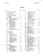
Page 5: ...ution 3 1 3 11 Panel Features 3 2 3 13 Operator s Checks 3 2 3 15 Operating Instructions 3 2 3 16 Front Panel FREQ CAL 3 2 3 18 Internal Leveling 3 3 External Crystal Detector Leveling 3 3 External Power Meter Leveling 3 3 External Frequency Modulation 3 3 External Amplitude Modulation 3 4 RF Power Control 3 4 Option 002 Step Attenuator 3 4 Alternate Sweep Mode With Option 002 3 4 Phase Lock Opera...

Page 6: ...2 Point Location 5 11 Delay Line Discriminator 1 11 5 5 YO Driver Board Adjustment Interface Signals on Connector P1 2 2 Test Setup 5 12 Interface Signals on Connector P2 2 3 5 6 YO Driver Board Test Points 5 13 Packaging for Shipment Using 5 7 Front Panel Hexadecimal Factory Packaging Materials 2 5 Entry Keys 5 13 Simplified Tuning Voltage 5 8 Test Setup for Frequency Block Diagram 3 2 Accuracy A...

Page 7: ...0 Rear Panel Connector Alignment Diagram 8 11 83522A RF Plug in Simplified Block Diagram 8 25 83522A RF Plug in Overall Block Diagram 8 25 Display Test Pattern 8 26 A1 Front PanelIA2 Front Panel Interface Block Diagram 8 31 A1 Front Panel Component Locations 8 31 A2 Front Panel Interface Component Locations Front View 8 31 A2 Front Panel Interface Component Locations Rear View 8 31 Column Strobing...

Page 8: ...le Page Table Page 1 1 Specifications for Model 83522A 6 2 Manufacturers Code List Reference Installed in Model 8350A 1 3 Designations and Abbreviations 6 2 1 2 Supplemental Performance Characteristics 6 3 Replaceable Parts 6 5 for Model 83522A Installed in 8 1 Index of Service Sheets 8 2 Model 8350A 1 4 8 2 Error Codes Associated With 83522A 8 6 Service Accessories Available 1 7 Recommended Test ...

Page 9: ...e like which if not correctly performed could result in personal injury Do not proceed beyond a WARNING sign until the indicated conditions are fully understood and met The CAUTION sign denotes a hazard It calls attention to an operating procedure practice orthe like which if not correctlyperformed oradhered to could result in damage to or destruction of part or all of the product Do not proceed b...

Page 10: ...General Information Model 83522A Figure 1 1 Model 8352214 RF Plug in ...

Page 11: ...I General Information ...

Page 12: ...r all parts and assemblies g SECTION VII MANUAL BACKDATING CHANGES provides backdating informa tion required to make this manual compat ible with earlier shipment configurations h SECTION VIII SERVICE provides an overall instrument block diagram with troubleshooting and repair procedures Each assembly within the instrument is covered on a separate Service Sheet which contains a circuit description...

Page 13: ...ible Hewlett Packard recommends that you periodically request the latest Manual Changes supplement The supplement for this manual is keyed to the manual s print date and part number both of which appear on the title page Complimentary copies of the Manual Changes supplement are available on request from Hewlett Packard 1 15 For information concerning a serial number prefix that is not listed on th...

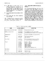
Page 14: ...Model 83522A General Information Table 1 1 Specifications for Model 83522A Installed in Model 8350A 1 of 2 ...

Page 15: ...tics included for user information FREQUENCY CHARACTERISTICS c c u r a c y Stability with Temperature k200 kHz C 25 C If 5 C CW Mode typically 0 01 to 2 4 GHz k1 5 MHz OUTPUT CHARACTERISTICS Manual Sweep Power Output 0 01 to 2 4 GHz 140 MHz Resolution displayed 0 1 dB All Sweep Modes Sweep time 10 ms to 100 ms Remote Programming settable k25 MHz Typically k0 01 dB Sweep Mode ineearit Stability wit...

Page 16: ...B 10 MHz Markers f200 kHz 50 MHz Markers 300 kHz Calibrated a n e Up to 5 dB GHz Up to 15 dB for full sweep range External Markers f300 kHz Resolution displayed 0 01 dB GHz Temperature Stability Typically t 2 X 1 0 MODULATION CHARACTERISTICS GENERAL CHARACTERISTICS External A M External Marker Input Generates amplitude or Z axis marker when sweep frequency equals external Frequency Response Typica...

Page 17: ...pplica tions The Model 8410Bl8411A Network Analyzer utilizes this output in such a configuration 1 24 The RF output may be turned off by the RF ON OFF pushbutton RF power on is indicated by the LED in the center of the pushbutton Additionally in CW mode the CW FILTER when selected places a capacitor across the YIG oscillator tuning coil to filter high frequency noise which would appear at the RF o...

Page 18: ...s from 110 MHz to 18 GHz The Model 8350A 83522Acombination is capable of operation from 110 MHz to 2 4 GHz within this range The Model 8410B has an Auto Frequency Table 1 3 Service Accessories A vailable NAME 44 pin printed circuit board extender RF Plug in Extender Cables Adjustment Tool Wrenches Service Cables Adapters Hex Balldriver IC Test Clip These items are included in a Service Accessories...

Page 19: ...ut eliminating unnecessary cable connections to the Model 8755 or the use of an external modulator The Model 8350A can also produce alternate sweeps through use of the ALT n function which works in conjunction with the channel switching circuits in the Model 8755C This permits Channel 1 on the Model 8755C to respond only to the Model 8350A current state and Channel 2 to the alternate state A singl...

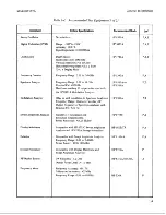
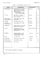
Page 20: ...Div X vs Y Display Mode Frequency Range 0 01 to 2 4 GHz Frequency Range 0 01 to 18 GHz Residual FM GI00 Hz Must have auxiliary IF output when used with the HP 8901A Modulation Analyzer May be used in addition to Spectrum Analyzer Frequency Range Must cover auxiliary IF Output frequency of Spectrum Analyzer used Residual FM lo Hz Capable of Transmission and Reflection measurements Power Resolution ...

Page 21: ... from 100 kHz to 10MHz Power Range 20 to 10 dBm No substitute when used for external power meter leveling Frequency Range 0 0 1 to 2 4 GHz Maximum SWR 1 75 Power Range 1 yW to 100 mW Frequency Range 0 01 to 2 4 GHz Frequency Response 0 01 to 2 4 GHz Maximum Input Power 100 mW Attenuation 10 0 5 dB Frequency Range 0 01 to 2 4 GHz Maximum Input Power 2 20 dBm Type N Connector Frequency Range 0 0 1 t...

Page 22: ...2 required Delay Line 1 meter 3 feet in length SMA male connectors Adapter BNC Female to Male SMA Mixer Double Balanced 1 to 12 GHz RHG Electronics Part No DM 1 12 1 to 18 GHz RHG Electronics Part No DM 1 18 RHG Electronics Laboratories Inc Deer Park NY 11729 Adapter SMA Male to SMA Male HP Part Number HP 11667A 1250 1250 08503 20038 1250 1200 1250 1159 ...

Page 23: ...II Installation ...

Page 24: ...figuration switch A3S1 located on the A3 Digital Interface Board This switch must be preset prior to RF Plug in operation in the Model 8350A The configuration switch is an 8 section multiple switch Each of the separate switches o r r o n d s to a separate RF plug in function such as FM sensitivity selection FM modulation input coupling selection direct coupled or cross over RF power level at power...

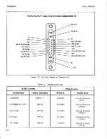
Page 25: ...TURN SENSE V TUNE 4 83522A Connector Connector Name J1 RF INPUT 52 EXT MTR ALC INPUT 53 EXT MKR 54 lV GHz J5 PULSE IN Mating Connector o o O O O 0 1 5 0 013 0 Industry Identification TYPE N f BNC 0 BNC f BNC 0 BNC f HP Part No 1250 0882 1250 0256 1250 0256 1250 0256 1250 0256 Alternate Source Specialty Connector 25 P117 2 Specialty Connector 25 P118 1 Specialty Connector 25 P118 1 Specialty Connec...

Page 26: ...Model 83522A Installation PLUG IN INTERFACE CONNECTOR P2 Figure 2 2 Interface Signals on Connector P2 2 3 ...

Page 27: ...le downward while still pushing in on the RF plug in until the drawer latch is fully closed and the front panel of the RF plug in is aligned with the sweep oscillator front panel 2 21 STORAGEANDSHIPMENT 2 22 Environment 2 23 The instrument may be stored or shipped in environments within the following limits Temperature 40 C to 75 C Humidity 5 to 95 relative at 0 to 40 C Altitude Up to 15240 meters...

Page 28: ...Factory Packaging Materials TWO PLACES C D 6 5 6 3 6 HP Part Number 9211 3515 9211 3514 9220 3409 9220 3406 9222 0352 Item 1 2 3 4 Not Shown Description Outer Carton Inner Carton Side Pads Corrugated Cardboard Foam Pads Poly Bag to cover instrument Quantity 1 1 2 2 1 ...

Page 29: ...III Operation ...

Page 30: ...AC and the sweep width is deter mined by the AF DAC DAC Used CF Vernier AF 1 118of band AF 118 1 64of band AF 1 64 of band 3 7 The CF DAC has 12 bits hence 4096 points across the plug in frequency band including overrange The analog output ranges from zero to ten volts which is used to coarsely specify the center frequency output of the plug in These parameters give the CF DAC a resolution of 0 02...

Page 31: ...F values vary with sweep width Figure 3 2 illustrates the AF mode displayed resolution values versus displayed AF frequency sweep widths 3 13 OPERATOR S CHECKS 3 14 The Operator s Checks local and remote in the 8350A Sweep Oscillator manual provide a quick evaluation of 8350A and 83522A main functions Error codes 50 to 99 indicate plug in related problems The 8350A Local Check covers the sweep osc...

Page 32: ...stead of a power splitter to sample the RF signal for the leveling loop Directional couplers are usually narrow band whereas the power splitter is flat over a wide frequency range The advantage of a directional coupler is that it does not have the 6 dB loss like the power splitter therefore a higher maximum leveled power output may be obtained Figure 3 6 illustrates a typical crystal detector leve...

Page 33: ...voltage causes an increase in RF output power 3 29 RF Power Control 3 30 The RF power selected at power up Instrument Preset may be either maximum power 4 13 dBm or power OFF as chosen on the configuration switch A3S1 refer to Figure 3 8 for this setting The configuration switch also has switch settings for the model plug in and use of Option 002 Step Attenuator The config uration switch settings ...

Page 34: ...itude mode power per sweep dB SWP 8 Power meter automatic leveling control selec 19 POWER LEVEL allows setting of output power tion HP 432 only for all ALC modes may be calibrated for 9 External crystal detector automatic leveling external leveling control selection negative crystal output 20 SLOPE allows setting of the frequency slope 10 Internal leveling control selection compensation in dB GHz ...

Page 35: ... EXT MKR 1V RMS MAX input connector 5 EXT ALC connector replaces front panel EXT ALC connector on Option 004 plug ins allowsuseof external marker when plug in EXT marker is engaged 6 Serial Number Plate has a ten digit serial number used in any correspondence con 3 PULSE IN connector is used to input external cerning plug in and Option number if pulse or squarewave modulation applicable Figure 3 4...

Page 36: ...ENCY switches on 3 Adjust FREQ CAL control until MKR lamp is on 4 Press 8350A 1 0 5 Press 83522A 10 MHz Marker 6 Fine adjust FREQ CAL control if needed until MKR lamp is on 7 Press 83522A Marker 8 A small adjustment of FREQ CAL control may be needed for MKR lamp to light Figure 3 5 Front Panel FREQ CAL Procedure 3 7 ...

Page 37: ...P 84914 Option 010 BNC Tee HP 1250 0781 PROCEDURE NOTE Crystal output signal must be between 10 mVdc and 200 mVdc 1 Connect equipment as shown in test setup b OSClLLOSCOPE SWEEP RF POWER Figure 3 6 External Crystal Detector Leveling 1 of 2 OSCILLATOR PLUG IN o i O O C O o pamn 8 gE1E8 o ooo o bg om 00 00 8 0 0000 a q lilmm 0y O 0 i 9 0000 9 0 0 0 METER EXT MTRlALC INPUT A B 6NC VERT RF 0UTPUT TEE ...

Page 38: ...e test setup The circuit may be inserted in the line to the EXT INPUT of the RF Plug in BNC M TO DUAL BANANA POST HP 10110A TO EXT MTRlALC INPUT SEE DETAIL A TO CRYSTAL DETECTOR 2 Switch on 8350A LINE switch Press WSTR PWSET key The START and STOP indicators should be on 3 Set controls as follows 83522A ALC MODE EXT 4 Adjust EXTIMTR ALC CAL for a power meter reading equal to the front panel output...

Page 39: ...or HP 8350A RF Plug in HP 83522A Power Meter HP 432A Thermistor Mount HP 8478A Oscilloscope HP 1740A Crystal Detector HP 423B 10 dB Attenuator HP 84914 Option 010 Power Splitter HP 11667A NOTE For power meter leveling sweep rates should be slower than 50 seclsweep to ensure proper leveling due to the slow response of the thermistor mount The HP 435 and 436 power meters will not power meter level t...

Page 40: ...3 39 The 8350A FREQUENCY display will indicate RF plug in error codes 50 to 99 or sweep oscillator error codes Information on plug in error codes may be found in Section VIII Service of this manual 3 40 Fuses 3 41 Power circuits for the Model 8352211RF Plug in are fused in the 8350A Sweep Oscillator See the 8350A Sweep Oscillator Operating and Service Manual for fuse locations and replace ment ins...

Page 41: ... 4 Switches with t should not be changed from Factory setting Switch Number Description 1 2 3 4 5 6 7 8 I t o d e for 83522APlug in Note 4 0 0 0 X X X X X RF Power Off at Instrument Preset X X X 1 X X X X Maximum RF Power at X X X O X X X X Instrument Preset 6 MHz V FM Sensitivity 20 MHz V FM Sensitivity Direct CoupledFM Note 3 Crossover Coupled FM tep Attenuator Option 002 Installed Note 4 No Ste...

Page 42: ...IV Performance Tests ...

Page 43: ... 2 provides a tabulated index of the performance tests their acceptable limits and a column for recording actual measurements 4 8 The test procedures in Section IV of the 8350AOperating and ServiceManual frequently refer the operator to the Test Record Card in this section IVieasurement conditions unique to this plug in are tabulated under the columns entitled STEP and TEST CONDITIONS The number i...

Page 44: ...RYSTAL MARKERS SPECIFICATION Conditions RF power level i 3 to i 13 dBm 510 markerslsweep Harmonic markers of 10 and 50 MHz are available up to 2 4 GHz 1 MHz harmonic markers are available below 1 GHz Markers are available as intensity spots or as amplitude dips on the RF output DESCRIPTION The RF output is detected and displayed on a CRT Sweep widths are selected to accomodate 10harmonic markers g...

Page 45: ...50A CF Press 83522A Monitor markers while slowly rotating the left RPG until CF equ erify that amplitude markers are equally spaced and stable across the frequency band 1 0 MHz Markers 7 On the 83504 press CF and at DATA ENTRY enter 60 MHz Press bF and at enter 100MHz Onthe 835224 press MHz markers a 8 Verify the presence of 10 equally spaced and stable markers 9 On the 83504 press CF Monitor mark...

Page 46: ... NOTE For Opt 002 extend upper and lower limits in step 13 by 0 2 dB Max Leveled Power 13 dBm Internal Leveled k0 25 dB Power Sweep 1 1 5 dB SWP procedures STEP 4 5 6 8 8A 9 12 9 12 13 15 17 for the following tests are found in the TEST CONDITIONS NOTE Perform FREQ CAL adjustment in Section Ill before proceeding with test Start frequency 10 MHz Stop frequency 2 4 GHz CW frequency 10 MHz CW frequen...

Page 47: ... 12 MHz Cross Over Coupled DC 100 Hz f 75 MHz Direct Cross Over coupling 100 Hz 1 MHz f 7 MHz 1 2 MHz f5 MHz 2 10 MHz f 1 MHz STEP 2 3 4 5 7 9 10 13 14 2 5 3 6 3 5 1 3 4 9 10 11 TEST CONDITIONS CW frequency 1 0 GHz Low line voltage High line voltage Power 13 dBm CW frequency 1 00 GHz Power 13 dBm CW frequency 1 0 GHz Reduce power to 3 dBm Power 13 dBm CW Frequency 1 3 GHz CW frequency 1 GHz In dB ...

Page 48: ...y 10 dB f0 5 dB 20 dB k0 7 dB 30 dB k0 9 dB 40 dB 1 2 dB 50 dB f1 5 dB 60 dB f 1 8 dB 70 dB f2 1 dB NOTE The procedure for the following test is found on the pages immediately preceding this test card STEP 5 1 3 4 1 4 10 MkrsISWP 10 MkrsISWP 10 MkrsISWP 10 MkrsISWP 10 MkrsISWP 10 MkrsISWP 4 1 6 Internal Crystal Markers 3 to 4 13 dBm 110mkrs SWP 50 MHz 10MkrsISWP 2 4 GHz 10MHz 10MkrsISWP 2 4 GHz 1 ...

Page 49: ...V Adjustments ...

Page 50: ... is aware of the hazard involved Capacitors inside the instrument may still be charged even if the instrument has been disconnected from its source of supply Use a non metalic adjustment tool when ever possible 5 5 EQUIPMENT REQUIRED 5 6 Table 1 4 lists the equipment required for the adjustment procedures If the test equipment recommended is not available other equipment may be used if its perform...

Page 51: ...ower meter leveling calibration Sets the gain of the main ALC amplifier Adjusts for zero offset through U7 Q6 log amplifier circuit Adjusts for zero offset through U5 log amplifier circuit Adjust for zerooffset through U8 Q1 Sampleand Hold circuit Adjust for zero offset through U11 Main ALC amplifier Adjusts low frequency for best frequency response flatness through U10 Sets balance of U10 video a...

Page 52: ...forALC flatness Slope adjustment for best ALC flatness Slope adjustment for best ALC flatness Slope adjustment for best ALC flatness Slope adjustment for best ALC flatness Sets overall slope of internal leveling ALC Sets range for power sweep Works in conjunction with C14 to set frequency response flatness of ALC Fine adjustment of tuning voltage from the scaling DAC Sets 10 Volt reference Adjusts...

Page 53: ...sts bias of the internal mixer when 1 MHz marker is selected Adjusts bias of the internal mixer when 10MHz marker is selected Adjusts bias of the internal mixer when 50 MHz marker is selected Sets gain of video amplifier U1 when 1 MHz marker is selected Setsgain of video amplifierU1 when the 10MHz marker is selected Sets gain of video amplifierU1 when the 50 MHz marker is selected Setsgain ofvideo...

Page 54: ...hms 5 to 12 pf Typ 3160 Ohms Max 5110Ohms Basis of Selection Selects scalingof current drive of YIG Oscillator FM coil near 100kHz Selected at factory to correct for frequency nonlinearity in YIG Oscillator A12 Allows maximum marker OFF pulse without overlappingthe ON pulse Center the range of 50 mHz frequency adjustment Minimizes feedthrough of 27 8 kHz square wave into the external marker birdie...

Page 55: ... 22K 4 64K 5 11K 5 62K 6 19K 6 81K 7 50K 8 25K 9 09K 10 OK 11 OK 12 1K 13 3K 14 7K 16 2K 17 8K 19 6K HP Part Number 0698 0082 0757 0416 0757 0417 0757 0418 0757 0419 0757 0420 0757 0421 0757 0422 0757 0280 0757 0424 0757 0274 0757 0317 0757 1094 0757 0428 0757 0278 0698 0083 0698 0084 0698 3150 0698 0085 0698 3151 0757 0279 0698 3152 0698 3153 0698 3154 0698 3155 0757 0438 0757 0200 0757 0290 0757...

Page 56: ... 20 5 21 5 22 5 23 5 24 5 25 5 26 5 27 5 28 2 Performthe FollowingParagraph Number 5 17 5 19 5 13 5 20 thm 5 24 5 20 t h r 5 26 5 14 thru 5 17 s 19 5 14 5 16 5 18 5 27 5 17 5 27 5 28 5 14 s 15 5 16 5 19 5 20 thru 5 24 5 26 5 20 thru 5 24 5 20 t h r 5 24 5 20thru 5 24 5 20 thm 5 24 5 20 thm 5 24 Adjustments I Configuration Switch A3S1 Oscillator Bias on A7 lOV Reference on A6 YO Driver YO Driver Bo...

Page 57: ... procedures and performance tests all assume that A3S1 is set to the factory setting If other procedures are to be performed set A3S1 to the factory setting until the procedures are completed then set A3S1 to the desired operating mode before putting the instrument back in service 1 Refer to Table 5 6 and determine if factory selected mode set at A3S1 is correct foryour application 2 Set configura...

Page 58: ...led No Step Attenuator Option 002 Installed Switch Number 1 0 x x x x x x x x NOTES 1 Switch Positions 1 Switch Open High 0 Switch Closed Low Ground x Don t Care 2 Switch A3S 1is set from the factory as follows A3S1 2 0 x x x x x x x x Switch NO 1 2 3 4 5 6 7 8 3 0 x x x x x x x x Position 0 0 0 0 0 0 x 1 2 3 4 5 6 7 8 A3 I if Opt 002 installed 0 if Opt 002 not installed OPEN 1 BOARD CLOSED O 4 x ...

Page 59: ......

Page 60: ... is used as OFFSET REF for the power level reference circuit EQUIPMENT Sweep Oscillator HP 8350A Digital Voltmeter DVM HP 3455A PROCEDURE 1 Connect DVM to A6TP3 10V REF and common to A6TP5 Figures 5 3 and 5 4 2 Adjust 10 control A6R21 for 10 000 Vdc k0 001 Vdc SWEEP OSCILLATOR 1 1 DIGITAL VOLTMETER Figure 5 3 1 0 Volt Reference Test Setup GND ANLG lOV REF A6TP5 1 0 A6R21 A6TP3 Figure ion ...

Page 61: ...quency accuracy and sweep linearity across the band If frequencies are within 5 MHz tolerance do not make these YO Driver Board adjustments 1 Connect the equipment as shown in Figure 5 5 with the DVM connected to A6P1 pin 4 FREQ CAL and common connected to A6TP5 GND ANLG SWEEP RF OSCILLATOR PLUG IN DIGITAL VOLTMETER Figure 5 5 YO Driver Board Adjustment Test Setup 2 Press INSTR PRESET 3 Adjust the...

Page 62: ...e 5 6 YO river Board Test Points 5 Press then DATA ENTRY of 2 4 GHz NOTE SHIFT 00 selects data entry making key M I function as address code entry and key M2 as data code entry 6 Press gg5m then DATA ENTRY of 00 7 Make DATA ENTRY of 2C80 Refer to HEX entry key diagram in Figure 5 7 for location of C DATA ENTRY SHIFT F Figure 5 7 Front Panel Hexadecimal Entry Keys ...

Page 63: ...e as the adjustments are made If 6 250 f 0 010 Vdc cannot be achieved when adjusting A6R11 G in step 12 set it as close as possible and note this value for use in step 16 13 Press mthen DATA ENTRY of FF 14 Press to shift address to 2C81 15 Press 8 then DATA ENTRY of 4F 16 Add 12 9968to the value previously noted in step 12 If the voltage in step 12was set to exactly 6 250 Vdc this new value would ...

Page 64: ...isplayed on the front panel FREQUENCY display as the RF output frequency is monitored with a frequency counter This error code is then entered into the A6 calibration switches A6S1 for the low end and A6S2 for the high end After the frequency accuracy is set the 50 MHz markers are roughly checked for accuracy at the center of the band within the range of the the FREQ CAL control EQUIPMENT Sweep Os...

Page 65: ...scillator Output and Adjustments Frequency Accuracy Calibration 2 Connect equipment as shown in Figure 5 8 with frequency counter and 10 dB attenuator connected to RF OUTPUT Connect the DVM to A6P1 pin 4 FREQ CAL and common to A6TP5 GND ANLG 3 Press IRSTR PIKESET 4 Adjust CAL knob for a DVM reading of 0 000 f 0 010 Vdc This sets the FREQ CAL adjustment to the electrical center of its range 5 Press...

Page 66: ...1 Press RECACL 1 and 50 MHz should be displayed 12 Press SHlFl then 90 This selects low end frequency calibration mode 13 Adjust P OWER RPG control for a reading of 50 MHz on external frequency counter 14 Set switch A6S1 Figure 5 10 for the value displayed in POWER window Refer to the diagram in Figure 5 11 GAIN A6S2 FRONT OFFSET A6S1 Figure 5 10 Frequency Calibration Adjustments Location ...

Page 67: ...2 400 GHz should be displayed TO FRONT OF PLUG IN DEPRESSED SWITCH POSITION 9 8 7 6 5 4 3 2 1 0 y 3r5 w4tl i 18 Press SH FT then 91 This selects high end frequency calibration mode 19 Adjust RPG control for a reading on the external frequency counter of 2 400 GHz u o C I i 20 Set A6S2 Figure 5 10 for the reading displayed in the POWER window C 21 Press MSm PRESET then RECALL 2 22 Verifythat a sett...

Page 68: ... sweep speeds The Frequency Calibration procedure is first done to ensure that the proper frequencies are referenced during the adjustment procedure An 8350A amplitude marker is used as the frequency reference which will not change as sweep time is modified At a slow 0 5 second sweep time the 8350A amplitude marker is set adjacent to an 83522A 50 MHz crystal marker at the frequency of interest Swe...

Page 69: ...83504 select CW mode and with the DVM measure and note the voltage at A6TP6 DELAY COMP 4 Press wm then XF At DATA ENTRY enters 5 Adjust A7R47 Z for the same reading at A6TP6 as was obtained in step 3 Refer to Figure 5 13 for the adjustment location Remove the DVM test leads 6 On the 8350G press ewQ 7 j 7 On the 835224 press wmP Twm 50 MHz Marker Frequency switches on automatically at Instrument Pr...

Page 70: ...sary for the MKR lamp to light The RF output fr crystal marker frequency is now calibrated accurately Do not change the position of the FREQ CAL control for the remainder of the test or the frequency calibration will be lost 14 the equi ment as sho 83504 press t h e n M1aC5 OSCILLOSCOPE SWEEP RF OSCILLATOR PLUG IN Figure 5 14 Delay Compensation Adjustment Test Setup SWEEP POS Z BLANK 0UTllN CH A C...

Page 71: ...the sweep speed is decreasedto 10 milliseconds 17 On the 83504 press Rotate the VERNIER to place the third crystal marker 150 MHz marker exactly 0 4 divisions to the left of the leading edge of the 8350A amplitude marker as shown in Figure 5 15 It may be necessary to fine adjust the oscilloscope horizontal position control and the Channel A vertical position control to move the leading edge of the...

Page 72: ...r greater than 1 6 GHz 23 On the 83504 press Rotate the 8350A FREQUENCYITIME vernier to place the marker near center screen on the oscilloscope Temporarily removing the oscilloscope fromXI0 magnification will aid in findingandmovingthe marker Resetthe oscilloscope to XI0 magnification before proceeding 24 On the 83504 press Rotate the VERNIER to place the desired crystal marker exactly 0 4 divisio...

Page 73: ...Hz output Example 1 GHz 1 Volt 2 4 GHz 2 4 Volts etc EQUIPMENT Sweep Oscillator HP 8350A Digital Voltmeter HP 3455A PROCEDURE NOTE Frequency accuracy must be adjusted accurately Paragraph 5 17 before adjusting Frequency Reference 1 V GHz output 1 Connect a DVM to A2TPl Figure 5 16 OFFSET GAIN YO DRIVE V A2R4 A2R1 A2TPl BAND 0 OFFSET A2R6 FRONT PANEL INTERFACE A2 FRONT Figure 5 16 Frequency Referen...

Page 74: ...JUSTMENT NOTE Complete adjustment of the leveling loop requires several proceduresto be performed in the order prescribed from Paragraph 5 20 through 5 24 Deviation from this routine may cause improper leveling and or flatness problems REFERENCE Performance Test 8350A Paragraph 4 14 Service Sheet A4 DESCRIPTION Adjustments compensate for DC offsets in the detected RF path and the Main ALC amplifie...

Page 75: ... kHz square wave modulation is selected 1 Remove A5 FM Driver board Place A4 assembly on an extender board Set A4R1 SLP fully counterclockwise Sweep the full range of the plug in at any leveled power 2 Connect the digital voltmeter to A4TP12 with floating ground on A4TP14 Refer to Figure 5 18 Adjust A4R47 OFS 1 offset 1 for 0 000V f 0 001V SWEPT AMPLITUDE SWEEP RF ANALYZER OSCILLATOR PLUG IN DIGIT...

Page 76: ... to A4TP15 floating ground Adjust A4R67 OFS 4 offset 4 for 0 000V f 0 001V 6 Set CW frequency to 50 MHz Turn off power Connect DVM to A4TP10 and adjust A4R4 BIAS for 0 000V 0 001V TuA on power 7 Turn instrument power OFF Remove A4 asse m the extender board and reinsert A4 d into the instrument Turn ON power to instrument Connect power meter to 83522A RF OUTPUT for plug in front panel reading of O ...

Page 77: ...ent of the leveling loop requires several proceduresto be performed in the order prescribed from Paragraph 5 20 through 5 24 Deviation from this routine may cause improper leveling andlor flatness problems REFERENCE Performance Test 8350A Paragraph 4 14 Service Sheet A5 DESCRIPTION Four parallel circuits on the A5 assembly provide adjustments for ALC flatness BPI through BP4 and SLl through SL4 de...

Page 78: ...he full range of the plug in SWEEP RF OSCILLATOR PLUG IN SWEPT AMPLITUDE ANALYZER 1111 8 1111 1181 1 1 1 B ATTENUATOR DETECTOR 0 o 0 0 Figure 5 19 Internal Leveling Adjustment Setup NOTE The following step negates any flatness compensation by effectively removing the ALC Flatness Adjustments from the leveling circuitry This step may be omitted if RF flatness approaches specified limits 2 Adjust al...

Page 79: ...ll flatness BPI and SLl are interdependent adjustments as are BP2 and SL2 etc The breakpoint potentiometers determine the frequency at which the slope adjustments will take effect This is observed as a pivot point on the CRT trace NOTE Ifflatness does not meet specification and some or all of the breakpoint and slope adjustments are ineffective center all nine potentiometers and repeat the procedu...

Page 80: ...sor HP 8481A PROCEDURE NOTE This procedure assumes that A3S1 is set to the factory set position Table 5 6 and at the 8350A Sweep Oscillator 27 8 kHz square wave modulation is selected 1 Connect equipment as shown in Figure 5 21 with the 8755C monitoring the RF output Select 8350A Observe the full band trace and select a frequency where the power level is ately nter of the power variation range Sel...

Page 81: ...on from 0 dBm should be equal and opposite If not readjust A4R6 0 LO 3 Set power for front panel indication of 9 dBm Adjust A4R7 0 MD for RF OUTPUT power at the 83522A connector of 9 dBm f 0 1 dBm 4 Iterate steps 2 and 3 until low and midpower ranges are calibrated 5 Set power for front panel indication of 13 dBm Adjust A4R2 0 HI for RF OUTPUT power at the 83522A connector of 13 dBm k0 1 dBm 6 Ste...

Page 82: ...entiometer A4R9 PM calibrates loop gain to full scale deflection of the leveling meter EQUIPMENT Sweep Oscillator HP 8350A Power Meter HP 432A Thermistor Mount HP 478A 10 dB Attenuator HP 8491A Option 010 PROCEDURE NOTE If during the following procedure ALC loop oscillations occur reduce loop gain by adjusting A4R11 Figure 5 26 counterclockwise This adjustment will be set in the next procedure 1 e...

Page 83: ...for a power me 3522A front panel power indication should be approximately 10 dBm 5 Iterate between power level settings of 5 and 10 dBm adjusting the knob and A4R9 respectively until no further adjustment is necessary PM POWER METER A4R9 Figure 5 24 Power Meter Leveling Adjustment Location 5 24 ALC GAIN ADJUSTMENT NOTE Complete adjustment of the leveling loop requires several proceduresto be perfo...

Page 84: ...uator HP 8491A Option 010 PROCEDURE NOTE This procedure assumes that A3S1 is set to the factory set position Table 5 6 1 Connect equipment as shown in Figure 5 25 OSCILLATOR PLUG IN CRYSTAL POWER MOUNT THERMISTOR Figure 5 25 ALC Gain Adjustment Test Setup 2 Press 8350A 3 On the oscilloscope select A versus B mode to display a plot of frequency versus amplitude Set the Channel A vertical sensitivit...

Page 85: ... slightlyto eliminate oscillations and obtain a focused dot trace GAIN A4Rll Set the switch ensure A4R11 Figure 5 26 ALC Gain Adjustment Location 83522A to the maximum leveled power by returning the power meter to the previous setting of 5 dB Observe the trace through the entire no oscillations at high power If oscillations occur reduce the gain by GAIN counterclockwise sweep to adjusting 10 Press...

Page 86: ...B Attenuator HP 8491A Option 010 PROCEDURE NOTE ALC gain adju atments paragraph 5 24 must be checked before power sweep adjustment are made NOTE This procedure assumes that A3S1 is set to the factory set position Table 5 6 and at the 8350A Sweep Oscillator 27 8 kHz square wave modulation is selected 1 Connect equipment as shown in Figure 5 27 Select 8350A fli fa n Figure 5 27 Power Sweep Test Setu...

Page 87: ...A5R50 23 Figure 5 28 Power Sweep Adjustment Location 5 26 FM DRIVER REFERENCE Performance Test 8350A Paragraph 4 21 Service Sheet A5 DESCRIPTION The FM Driver high frequency offset is adjusted for zero volt drive with no FM modulation applied A delay line discriminator is used to detect and display FM modulation on an oscilloscope Adjustments are for best overall frequency response from DC to 10 M...

Page 88: ...RE NOTE Turn AC power OFF when removing or installing PC boards NOTE This procedure assumes that A3S1 is set to the factovset position Table 5 6 FM Offset 1 Connect equipment as shown in Figure 5 29 except disconnect function generator from rear panel FM INPUT connector SWEEP OSCILLATOR I INPUT FM 1 SWEEP OUTPUT DIGITAL VOLTMETER OUTPUT DELAY LINE DISCRIMINATOR OSCILLOSCOPE FUNCTION GENERATOR 1 o ...

Page 89: ... HI FREQ FM OUTPUT PI 21 SELECTED VALUE A5R31 Figure 5 30 A5 FM Driver Adjustment Location 4 Disconnect DVM from test points remove extender board and reinstall A5 FM Driver in instrument 5 Set instrument controls as follows 8350A SWEEP OSCILLATOR CW FREQUENCY 1 2 GHz FREQUENCY Sweep Mode Pres CW VERNIER SWEEP TRIGGER INT RF BLANK OFF 83522A RF PLUG IN POWER LEVEL 13 dBm CW FILTER OFF ALC MODE INT...

Page 90: ...005V CHANNEL B INPUT DC CHANNEL B VIDIV 1 3 Flatness 6 Connect Frequency Counter to 83522A RF OUTPUT Connect a i 1 Vdc power supply to rear penel FM INPUT A shift in frequency of approximately 20 MHz should occur on the Frequency Counter when 1 Vdc is applied This shows correct FM modulation sensitivity Reconnect Delay Line Discriminator to RF OUTPUT and connect function generator to rear panel FM...

Page 91: ... point 3dB can be up to 5 6 divisions and minimum point 3 dB can be down to 2 8 divisions 11 If the flatness specification in step 10 above is not met repeat step 8 and 9 above and make compromise adjustments in the DC to 2 MHz range to meet flatness requirements MINIMUM 3 dB MAXIMUM 3dB Figure 5 31 FM Flatness Tolerance DC to 2 MHz 5 27 MARKERANDSAMPLERADJUSTMENTS REFERENCE Performance Test Parag...

Page 92: ...NOTE This procedure assumes that A3S1 is set to the factory set position Table 5 6 1 Place A8 assembly on extender board Connect equipment as shown in Figure 5 32 Terminate 83522A RF output in 50 Ohms Set 1740A Oscilloscope to A vs B sweep mode to obtain horizontal deflection as a function of the 8350A SWEEP OUT SWEEP A8 nc FREQUENCY OSCILLATOR COUNTER OSCILLOSCOPE RF PLUG IN zT 1 1RF OUTPUT I I s...

Page 93: ...A8R29 1M for the flattest envelope hei ht See Figure 5 34 Select tKlr Markers Adjust A8R30 IOM for the flattest envefope height Figure 5 33 Select 51 M E 3 2 markers Adjust A8R31 50M for the flattest envelope height Optimum setting for these adjustments will be ones that provide the most uniform birdie height acrossthe band with the adjustments nearest the center of their range Especially note bir...

Page 94: ...ust A7 Marker Threshold potentiometers for the proper pulse width of each marker as follows NOTE The previous step calibrates the oscilloscope display to 100 kHz Division 50 MHz Adjust A7R5 50M for 600 kHz p p 6 divisions 10 Mhz Adjust A7R6 10M for 400 kHz p p 4 divisions 1 MHz Adjust A7R7 1M for 200 kHz p p 2 divisions SELECTED VALUE A7R41e Figure 5 36 Marker Adjustments on A 7 ...

Page 95: ...ap The optimum value for A7R4 allows the maximum number of marker OFF pulses without overlapping the ON pulse The typical value for A7R4 is 1200 Ohms and the minimum value is 1000 Ohms To observe marker OFF pulses vary RF OUTPUT power between 3 dBm and 13 dBm Figure 5 37 On Off Pulse of Correctly Adjusted Circuit ONIOFF PULSE OVERLAP Figure 5 38 On Off Pulse of Misadjusted Circuit Showing Overlap ...

Page 96: ... Option 010 PROCEDURE NOTE This procedure assumes that A3S1 is set to the factory set position Table 5 6 and at the 8350A Sweep Oscillator 27 8 kHz square wave modulation is selected 1 Connect equipment as shown in Figure 5 39 Set external marker source to a selected marker frequency Set power level between 10 and 10 dBm RF MARKER SOURCE SWEPT AMPLITUDE ANALYZER OSCILLOSCOPE 10 dB ATTENUATOR Figur...

Page 97: ... at the output of A8Q2 may be obscuring the marker birdie Connect oscilloscope probe to A8TP4 Observe the birdie amplitude while turning the 8350A on and off If the modulation feedthrough obscures more than half o e peak value reduce 83522A output power The feedthrough level should decrease while the birdie amplitude should remain relatively constant The marker should appear on the 8755C If it doe...

Page 98: ...VI Replaceable Parts ...

Page 99: ...embly part number 6 5 ABBREVIATIONS 6 6 Table 6 2 lists abbreviations used in the parts list and schematics In some cases two forms of the abbreviation are used one all in capital letters and one partial or no capitals This occurs because the abbreviations in the parts list are always capitals However in the schematics other abbreviation forms are used with both lower case and upper case letters 6...

Page 100: ...ssemblies and components for this instrument The contents of the kit and the Recommended Spares list are based on failure reports and repair data and provides parts support for one year A complimentary Recommended Spares list for this instrument may be obtained on request and the Spare Parts Kit may be ordered through your nearest Hewlett Packard office Table 6 2 Manufacturers Code List Reference ...

Page 101: ... Ampere CONT Contact Continuous F ADJ Adjust Adjustment Control Controller ALC Alcohol Automatic CONV Converter F Fahrenheit Farad Level Control CP Cadmium Plate Candle Female Film Resistor AM Amplitude Modulation Power Centipoise Conductive Fixed Flange Flint AMP Amperage Plastic Cone Point Fluorine Frequency AMPL Amplifier CRP Crepe Crimp FEM Female ANLG Analog CS Case Centistoke Cesium FF Flang...

Page 102: ... Effect Transistor OD Olive Drab SNP Snap JFET Junction Field outside i STAT Status Effect Transistor OP Operational STL JGK Jade Gray Knob OPT Optical Option Optional SW Sing1e Switch HP 6009 0021 SZ Size P K T a PAN HD Pan Head TA Ambient Temperature KB Knob PC Picocoulomb Piece Tantalum L Printed Circuit TC Thermoplastic PCB Printed Circuit Board THD a Thread Threaded LED Light Emitting Diode P...

Page 103: ... LED VISIBLE LUM INT 7MCD IF 30MA MAX LED VISIBLE LUM INT 7MCD IF 3OMA MAX CONNECTOR50 PINMPOSTTYPE NUT HEX DBL CHAM 114 32 THD 094 IN THK NUT HEX DBL CHAM 114 32 THD 094 IN THK WASHER LK INTL T 114 IN 256 IN ID WASHER LK INTL T 1 4 IN 256 IN ID SPACER SPECIALTY 450 IN LG 175 IN OD CONNECTOR 50 PIN M POST TYPE RESISTOR 316 1 125W F TC Of 100 RESISTOR 316 1 125W F TC Of 100 RESISTOR VAR CONTROL CP ...

Page 104: ...125W F TC 0 100 RESISTOR lOOK 1 125W F TC Of 100 RESISTOR 40K 1 125W F TC Of 100 RESISTOR lOOK 1 125W F TC Of 0 0 RESISTOR 10K 1 125W F TC Of 0 0 RESISTOR lOOK 1 125W F TC Of 100 NOT ASSIGNED NOT ASSIGNED RESISTOR 1OK 1 05W F TC Of 100 RESISTOR 10K 1 05W F TC Ofl00 CONNECTOR SGL CONT PIN 04 IN BSC SZ RND CONNECTOR SGL CONT PIN 04 IN BSC SZ RND CONNECTOR SGL CONT PIN 04 IN BSC SZ RND IC OP AMP GP D...

Page 105: ...U F f 10 2OVDC TA CAPACITOR FXD 1 0 U F f 1 0 2OVDC TA CAPACITOR FXD O1UF f 2 0 100VDC CER CAPACITOR FXD 1UF f 2 0 50VDC CER CAPACITOR FXD l UF f 2 0 50VDC CER CAPACITOR FXD 33UF f 20 50VDC CER CAPACITOR FXD O1UF f 2 0 1OOVDC CER CAPACITOR FXD O1UF f 2 0 100VDC CER CAPACITOR FXD 1UF f 20 50VDC CER CAPACITOR FXD l UF f 2 0 5OVDC CER CAPACITOR FXD lOPF f 5PF 200VDC CER CAPACITOR FXD 1UF f 2 0 25VDC ...

Page 106: ...O NOT ASSIGNED RESISTOR 51 1 K 1 05W F TC OklOO RESISTOR 82 5K 1 05W F TC Of 0 0 RESISTOR 1 96K 1 05W F TC Of 100 RESISTOR 10K 1 05W F TC Of100 NOT ASSIGNED RESISTOR 5 62 1 05W F TC Of 100 RESISTOR TRMR 20K 10 C TOP ADJ 1 TRN C D 4 1 1 1 7 6 2 7 4 5 5 7 5 5 5 7 0 5 3 1 1 6 6 7 1 2 3 6 7 5 8 5 7 0 3 8 7 6 7 6 3 7 7 4 6 3 8 9 6 6 4 4 1 4 9 6 4 6 3 6 7 9 6 A4MP2 A401 A402 A403 A 4 0 4 A405 A406 A407 ...

Page 107: ...N M POST TYPE TERMINAL TEST POINT PCB TERMINAL TEST POINT PCB NOT ASSIGNED TERMINAL TEST POINT PCB TERMINAL TEST POINT PCB IC OP AMP LOW NOISE TO 99 IC SWITCH ANLG QUAD 16 DIP C IC OP AMP PRCN QUAD 14 DIP C IC MULTIPLXR 4 CHAN ANLG DUAL 16 DIP C IC OP AMP TO 99 IC MULTIPLXR 4 CHAN ANLG DUAL 16 DIP C IC OP AMP TO 99 IC OP AMP GP TO 99 IC SWITCH ANLG QUAD 16 DIP C IC GATE TTL LS NAND QUAD 2 INP IC O...

Page 108: ... f 5 300VDC MICA NOT ASSIGNED CAPACITOR V TRMR CER 4 5 20PF 160V CAPACITOR FXD O1UF f 20 100VDC CER CAPACITOR FXD O1UF f 20 1OOVDC CER CAPACITOR FXD O1UF f 2 0 lOOVDC CER CAPACITOR FXD O1UF f 20 1OOVDC CER NOT ASSIGNED CAPACITOR FXD 4 7PF f 2 5 P F 500VDC CER NOT ASSIGNED NOT ASSIGNED CAPACITOR FXD 1UF f 20 50VDC CER CAPACITOR FXD 1UF f 20 50VDC CER CAPACITOR FXD O1UF f 2 0 1OOVDC CER CAPACITOR FX...

Page 109: ... 0 RESISTOR 10 1 125W F TC Of 1 0 0 RESISTOR 10 1 125W F TC Of 1 0 0 RESISTOR 1 0 1 125W F TC Of 1 0 0 RESISTOR 10 1 125W F TC Of 1 0 0 NOT ASSIGNED RESISTOR 1K 1 125W F TC Of 1 0 0 RESISTOR 1K 1 125W F TC Of100 RESISTOR TRMR 1OK 10 C SIDE ADJ 1 TRN RESISTOR l K 1 125W F TC Of 0 0 RESISTOR 1K 1 125W F TC Of 0 0 TERMINAL TEST POlNT PCB TERMINAL TEST POlNT PCB TERMINAL TEST POlNT PCB TERMINAL TEST P...

Page 110: ...UFf10 1OVDC TA CAPACITOR FXD 6 8 U F f 1 0 35VDC TA CAPACITOR FXD 2 2 U F f 10 15VDC TA CAPACITOR FXD 022UF f 20 100VDC CER CAPACITOR FXD 1UF f 20 5OVDC CER DIODE SCHOTTKY DIODE SCHOTTKY DIODE GEN PRP 180V 200MA DO 7 DIODE GEN PRP 180V 200MA DO 7 DIODE GEN PRP 180V 200MA DO 7 DIODE GEN PRP 180V 200MA DO 7 DIODE GEN PRP 180V 200MA DO 7 RELAY REED 1A 500MA 1OOVDC 5VDC COIL INDUCTORRF CH MLD 3 6MH 5 ...

Page 111: ...5W F TC Of 1 0 0 RESISTOR 1K 1 125W F TC 0 100 SWITCH RKR DIP RKR ASSY 10 1A 05A 30VDC SWITCH RKR DIP RKR ASSY 10 1A 05A 3OVDC CONNECT R 16 PIN M POST TYPE NETWORK RES 10 SIP2 2K OHM X 9 NETWORK RES 10 SIP2 2K OHM X 9 IC DRVR TTL LS LlNE DRVR OCTL IC DRVR TTL LS LlNE DRVR OCTL IC COMPARATOR PRCN TO 99 IC SWITCH ANLG 8 DIP P IC DRVR TTL LS LlNE DRVR OCTL IC FF TTL LS D TYPE POS EDGE TRIG COM IC CON...

Page 112: ...CAPACITOR FXD 1UF 20 50VDC CER CAPACITOR FXD 3 3 U F f 1 0 10VDC TA CAPACITOR FXD 3 3 U F f 10 10VDC TA CAPACITOR FXD 1UF 20 50VDC CER CAPACITOR FXD 6 8 U F f 10 35VDC TA CAPACITOR FXD 6 8 U F f 10 35VDC TA CAPACITOR FXD 1 5 U F f 1 0 20VDC TA CAPACITOR FXD 1 5 U F f 10 2OVDC TA CAPACITOR FXD l UF f 2 0 50VDC CER CAPACITOR FXD 1000PF f 2 0 100VDC CER CAPACITOR FXD O1UF f 2 0 100VDC CER CAPACITOR F...

Page 113: ...ON ORDER BY DESCRIPTION TERMINAL TEST POlNT PCB TERMINAL TEST POlNT PCB ORDER BY DESCRIPTION ORDER BY DESCRIPTION SN74LS123N SW 02FQ MC34004BL SN74LSOON SN74 LSOON 3 IC M V TTL LS MONOSTBL RETRIG DUAL 2 IC SWITCH ANLG QUAD 16 DIP C 1 IC OP AMP LOW BIAS H IMPD QUAD 14 DIP C IC GATE TTL LS NAND QUAD 2 INP IC GATE TTL LS NAND QUAD 2 INP I IC OP AMP GP DUAL TO 99 1 IC M V TTL t S MONOSTBL RETRIG DUAL ...

Page 114: ...ONNECTOR RF SM SNP M PC 50 OHM 28480 1250 0543 A8J2 1250 0543 8 CONNECTOR RF SM SNP M PC 50 OHM 28480 1250 0543 A8L1 9100 2247 4 1 INDUCTORRF CH MLD 1OONH 10 105DX 26LG 28480 9100 2247 A8L2 9100 1626 1 1 INDUCTORRF CH MLD 36UH 5 166DX 385LG 28480 9100 1626 A8L3 9100 1693 2 1 INDUCTORRF CH MLD 360UH 5 2DX 45LG 28480 9100 1693 A8 L4 9100 2261 2 1 INDUCTORRF CH MLD 2 7UH 10 105DX 26LG 28480 9100 2261...

Page 115: ...4 2100 2514 0757 1094 0757 0438 0757 0438 0698 3260 0757 0466 0698 7260 0698 7248 0698 7212 0698 3452 0698 7236 2100 2514 0698 3447 1251 0600 1820 0306 1820 0475 1820 0306 1826 0811 1826 0610 1820 1383 1820 0804 1826 0092 1820 1383 1820 1730 1820 0809 1810 0279 1902 0025 0410 0594 83525 60010 0180 0291 0180 1735 1200 0043 1200 0043 83525 20034 83525 20036 2360 01 15 2360 01 15 2360 01 15 2360 01 1...

Page 116: ...C EDGE CONN RESISTOR 34 8K 1 125W F TC Of 1 0 0 RESISTOR 1 1 125W F TC Of 0 0 WIRE JUMPER NOT ASSIGNED NOT ASSIGNED CONNECTOR PC EDGE 22 CONT ROW 2 ROWS CONNECTOR PC EDGE 22 CONT ROW 2 ROWS CONNECTOR PC EDGE 22 CONT ROW 2 ROWS CONNECTOR PC EDGE 22 CONTIROW 2 ROWS CONNECTOR PC EDGE 22 CONT ROW 2 ROWS CONNECTOR PC EDGE 22 CONT ROW 2 ROWS CONNECTOR PC EDGE 6 CONT ROW 2 ROWS I NOT ASSIGNED I I I OSCIL...

Page 117: ...CONNECTOR RF BNC FEM SGL HOLE FR 50 OHM 1VIGHz CONNECTOR RF BNC FEM SGL HOLE FR 50 OHM PULSE IN NOTE SEE FIGURE 6 1 FOR MECHANICAL PARTS MP LOCATION MP1 MP2 MP3 MP4 THRU MP8 MP9 THRU MP19 COVER PC SEC WINDOW DISPLAY KNOB 3 4 JGK 25 IN ID NOT ASSIGNED KEY CAP QUARTER LlTE PIPE KNOB JADE GRAY KNOB JADE GRAY PANEL DRESS PANEL DRESS OPTION 004 ONLY KEY CAP HALF POWER LEVEL i I KEY CAP HALF POWER SWEEP...

Page 118: ...NED CABLE RF MODULATOR AMPLIFIER NOT ASSIGNED NOT ASSIGNED CABLE RF OSCILLATOR MODULATOR NOT ASSIGNED NOT ASSIGNED CABLE ASSY POWER SUPPLY CABLE ASSY REAR CONNECTOR CABLE ATTEN OUTPUT OPT 002 ONLY NOT ASSIGNED NOT ASSIGNED NOT ASSIGNED CABLE REAR PANEL RF OUT OPT 004 ONLY CABLE RF DETECTOR ATTENUATOR OPT 002 002 AND 004 CABLE ATTENUATOR REAR PANEL RF OUT OPT 002 and 004 CABLE YO MOD MIX OPTION 002...

Page 119: ...PI MP2 MP3 MP26 MP25 MP9 THRU MP19 UNDERNEATH MP24 MP23 OPT 004 MP31 THRU MP34 P37 MP46 MP38 THRU MP42 UNDERNEATH TYP 5 PLACES 0PT 004 NOTE Refer to Table 6 3 for mechanical parts listings Figure 6 1 Major Mechanical Parts 1 of 3 6 21 ...

Page 120: ...522A MP47 MP48 MP49 MP50 MP51 MP52 AND MP53 ON OPPOSITE SIDE MP54 MP58 MP57 MP55 STANDARD MP56 OPT 002 ONLY MP59 MP61 MP60 RIGHT SIDE NOTE Refer to Table 6 3 for mechanical parts listings Figure 6 1 Major Mechanical Parts 2 of 3 ...

Page 121: ...0 0105 2200 0107 2200 0147 2200 0149 2200 0166 0624 0281 0520 0127 0520 0128 0520 0136 0520 0167 0590 0106 0590 1126 2260 0009 2420 0001 2950 0001 2950 0132 2950 0177 2190 0016 2190 0068 2190 0104 1250 1142 3050 0003 4 6 O 2 8 2 4 6 4 6 7 3 6 7 7 4 8 4 3 5 8 6 9 3 5 O 5 3 12 4 6 5 16 2 2 10 4 2 2 30 4 4 4 2 4 1 8 6 4 1 1 5 1 1 1 5 HARDWARE LOCATIONS SCREW MACH 6 32 312 IN LG PAN HD POZI SCREW MACH...

Page 122: ...Replaceable Parts Model 83522A 1 R3522A RF PLUG IN 01 i i if TYP 4 PLACES TYP 4 PLACES _j Figure 6 2 Attaching Hardware 2 of 4 ...

Page 123: ...Model 83522A Replaceable Parts TYP 8 PLACES TYP 4 PLACES TYP 2 PLACES TYP 14 PLACES i Figure 6 2 Attaching Hardware 3 of 4 1 6 25 ...

Page 124: ......

Page 125: ...aceable Parts W10 DC RET DIR DET W25 MOD MIX AMPL W28 RF OSC MOD MIX W40 YO MOD MIX b W33 ATTEN RF OUT OPT 002 W38 DlR DET ATTEN 0PT 002 ATTEN REAR PANEL OPT 002 AND 004 W15 AMPL f DC RET Figure 6 3 Cables in RF Section ...

Page 126: ...ector Assy Type N 1 28480 1 86290 60005 I JlMPl 1 1250 1577 1 1 1 Body RF Connector Type N 05879 1 131 445 Contact RF Connector Type N Insulator Center Conductor Body Bulkhead Washer Lock 0 439 ID Nut Hex 7 16 28 Insulator 131 149 5040 0306 08555 20093 08555 20094 OBD OBD 08761 2027 Figure 6 4 RF Output Connector J l Exploded View 6 28 ...

Page 127: ...VII Manual Backdating ...

Page 128: ...configuration of the instrument Later versions of the instrument serial number prefixes higher that the one indicated on the title page are documented in a yellow Manual Changes Supplement 7 3 Since there are no earlier versions of the HP Model 83522A RF Plug in there is no change information provided here This manual applies directly to instruments with serial numbers prefixed as indicated on the...

Page 129: ...he title page of the manual This supplement contains important information for correctingmanual errors and for adapt ing the manual to instruments containing improvements made after the printing of the manual Two types of information are included UPDATES APPLY TO ALL SERIAL NUMBERS NUMBEREDCHANGES UPDATES THAT ARE SERIAL NUMBER PREFIX RELATED The information is in the followingorder UPDATES NUMBER...

Page 130: ... NEW ITEM INDEX ...

Page 131: ... New Assembly Part Number N A 8352540043 8352540060 83522 60061 83525 60068 8352240062 8352540072 83522 60077 83525 60080 N A 8352540092 83522 60098 83522 60084 Manual Sections Affected None Replaceable Parts Service Replaceable Parts Service Replaceable Parts Service Operation Replaceable Parts Service Replaceable Parts Service Replaceable Parts Service General Information Operation Adjustments R...

Page 132: ... HP Buyershall prepay shipping charges to HP and HP shall pay shippingcharges to return the product to Buyer However Buyer shall pay all shippingcharges duties and taxes for products returned to HP from another country LIMITATION OF WARRANTY The foregoing wannty shall not apply to defects resulting from improper or inadequate maintenance by Buyer Buyer supplied sofiwareor interfacing unauthorized ...

Page 133: ...ses wendet so ist vom Betreiber sicherzustellen dass die Funk Entstorbestimmungenunter Betriebs Model HP 83522A bedingungen an seiner Grundstucksgrenze ein gehalten werden Page 1 3 Table 1 1 Under Power Variation Internally Leveled add the followingspecification With Option 002 0 35 dB in 0dB attenuation step Deleteall referencesto Stability With Time in a 10minute period after one hour warmup Pag...

Page 134: ... 46 Paragraph 5 28 Delete Paragraph 5 28 on pages 5 46 through 5 48 and replace with 5 28 EXTERNAL MARKER ADJUSTMENT UPDATES contained in this document Page 6 1 Paragraph 6 7 Add the followingafier paragraph 6 7 Two Year Warranty and Restored Exchange Parts Themicrocircuit partslisted inTable6 0areprovided witheithera two yearwarranty fromthedateofpurchase and or a restored exchange parts program ...

Page 135: ...geA4R5Oto HP Part Number 0698 7274CD 3 RESISTOR 38 3K Mfr Part Number C3 1 8 TO 3832 G Page 6 15 Table 63 ChangeA7R48 to HP and Mfr Part Number 0698 3457 CD 6 316K recommendedreplacement Page 6 18 Table 63 ChangeA10J3 to HP and Mfi Part Number 1251 3196 CD 5 Page 6 19 Table 6 3 Change MP2 Part Number to 83522 20028 CD 5 Change MP27 to HP and Mfi Part Number 0050 2032 CD 9 Page 6 20 Table 6 3 Chang...

Page 136: ...ance test 8350A B Paragraph 4 14 Service Sheet A4 DESCRIPTION A4R15 in the input leg ofA4U9 adjuststhe gain ofthe MainALCAmplifier A4R15 is adjusted for maximum possible gain without producing oscillations EQUIPMENT Function Generator HP 3312A Oscilloscope HP 1740A Detector H P 8 4 7 3 C 10dB Attenuator HP 8491A Option 010 UPDATES SWEEP OSCILI ATOR 1EXT AM RF PLUG IN lodB ATTENUATOR I FUNCT lON GE...

Page 137: ...p p output on HP 331219 to 1740CHANNEL A INPUT 2 Set instrument controls as follows 8350AlB SWEEP OSCILLATOR START 10 MHz STOP 8 4GHz SWEEPMODE MANUAL 83522A RF PLUG IN POWERLEVEL 2dB ALC INT 3312A FUNCTIONGENERATOR MODULATION SWP MODULATION RANGE Hz KNOB a e 0 VERNIER 0 FUNCTION 1 1 RANGE Hz BUTTON lOOK FREQUENCY 5 AMPLITUDE 1 VERNIER 1 UPDATES APPLY TO ALL SERIALS UPDATES ...

Page 138: ...nd VERNIER to 10K 4 Connect equipment as shown in Figure 5 25 5 On 1740Aselect A vs B MODE and set CHANNEL A to OO5 DIV 6 Adjust the far left side of the signal for 2 divisions pk pk by using the CAL on the CHANNEL A knob 7 While monitoring CHANNEL A manually sweepthe entire plug in frequency range and adjust the ALC GAIN A4R15 for4 divisionsofpeaking at the plug in frequencywhere the highest gain...

Page 139: ...gderivativesofa 50 MHz crystaloscillatorwith the lowband sweep Propermarkerfunctioningrequiresadjustmentofthe crystaloscillator the internal mixer and IF gain for each marker frequency OSCILLATOR RF OUTWT TERMINATION FREQUENCY COUNTER OSCILLOSCOPE Figure 5 32 Marker Adjustments Test Setup 1 MHz 10 MHz 50MHz 1M 10M 50MBIAS A8R53 A8R54 A8R55 A8TP3 A8R29 A8R3O A8R31 Figure 5 33 Marker Adjustments on ...

Page 140: ...elect looms SweepTime Connect oscilloscope with 1 l capacitive probe to A8TP4 Set 8350A B power to 13dBm and select 1MHz Markers Adjust A8R29 for the flattest envelopeheight See Figure 5 34 Select 10MHz Markers Adjust A8R30 for the flattest envelope height Select 50 MHz Markers This waveform appears like a comb Adjust A8R31forthe flattestenvelopeheight Optimumsettingfortheseadjustmentswillbe ones ...

Page 141: ...5 27 MARKER AND SAMPLER ADJUSTMENTS UPDATES Cont d Figure 5 35 50 MHz Birdie nlllllllllllllllllllllln It C i i I Figure 5 36 Marker Adjustments on A 7 UPDATES UPDATES APPLY TO ALL SERIALS ...

Page 142: ...er ON pulses See Figure 5 37 While the crystal markers may function properly without them the marker off pulses provide a safeguard againstfalse markers appearing on the display 8 Secondly ensurethat the marker OFFpulsedoesnot overlapthe marker ON pulse Figure 5 38 illustrates an improper marker OFF pulse When this occurs change the value of A7R4to eliminateoverlap The optimum valueforA7R4allowsth...

Page 143: ...ector HP11664B 10dB Attenuator HP 8491B Opt 010 Oscilloscope HP 1740A FUNCTION GENERATOR SCALAR NETWORK ANALYZER 8NC TEE Figure 5 38a Marker Gain Fine Tune Adjustments Test Setup PROCEDURE 1 Connect equipment as shown in Figure 5 38a 2 Set instrument controls as follows 8350A B SWEEP OSCILLATOR CF 15MHz CF STEPSIZE 10MHz AF 10MHz LnMOD ON SWEEPTIME 17ms 83522A RF PLUG IN UPDATES POWER LEVEL 9 dBm ...

Page 144: ...just gain A8R53 However be awarethat theseadjustments can createdoublemarkers or degradation of off pulses 1MHz markers are only specified to 1 GHz CF ie correctly adjusted they may start disappearing or having double markersbeyond 1GHz 4 IterateStep3for 10MHz markerswith CF 60MHz CFSTEPSIZE 100MHz AF 100 MHz and the gain adjustment of ABR54 5 Reiterate Step 3 for 50 MHz markers with CF 260 MHz CF...

Page 145: ... HP 8755C Detector HP 11664B Oscilloscope HP 1740A 10dB Attenuator HP 8491A Option 010 RF MARKER SOURCE SWEEP OSCILLAT0R RF PLUG IN OUTPUT OUTPUT 10dB AITENUATOR 4 SWEPT AMPLITUDE ANALYZER DETECTOR I Figure 5 39 External Marker Adjustments Test Setup PROCEDURE NOTE ThisprocedureassumesthatA3S1issettothefactory set position Table5 6 and at the 8350AlB sweep oscillator 27 8 kHz square wave modulatio...

Page 146: ... value of resistor A8R28 until the marker appearson the screen However be aware that larger values of A8R28 will degrade the performance of the 8350AIB internal crystal markers Check the internal markers before permanently selecting a value for A8R28 Typical value is 3160 Ohms suggested maximum value is 5110Ohms NOTE If external marker harmonics interfere with the measurement reduce the marker sou...

Page 147: ...HP 83522A CHANGE 1 The 64 pinrearconnectorcableassemblyW32 isnowsolderedinsteadof crimped to minimizethepossibilityof intermittent open contacts The part number remainsunchanged CHANGE 1 1 111 2 ...

Page 148: ...86082 CD7 RESISTOR464 1 125WFTC O 2 100 Mfr Code24546 Mfr Part Number C4 118 TO 4640 F Page 8 51 Figure 8 40 Replace Figure 8 40 with A5 FMDriver ComponentLocations CHANGE2 fiom this document Page 8 51 Figure 8 43 Change the A5 FM DRIVER part number in the top left hand comer of the A5 Schematic to 83525 60043 Change the SERIALPREFIX in the bottom left hand comer of the page to 2202A Replaceblocks...

Page 149: ...A5 FM Driver Component Locations CHANGE 2 CHANGE 2 ...

Page 150: ... LOW FREQ SENSITIVITY SELECT AMPL R8 R I O 15VF I0K TP3 I L L O F M OFF 1 I SERIAL PREFIX 2202A P OA5 FM r b e r Schematic Diagram CHANGE 2 CHANGE 2 ...

Page 151: ...IG COM 01295 SN74LS273N Change MU10 to 1858 0069 Qty 1 CD 1 TRANSISTOR ARRAY 18 PINPLSTC DIP 13606 ULN 2803A Add A2W3 8159 0005 Qty 1 CD 0 RESISTOR ZERO OHMS 22AWG LEAD DIA 28480 81594005 Page 8 31 Figure 8 12 Replace the FRONT Component Locations diagram with the A2 Front Panel Inte ace Component Locations CHANGE3 diagram from this document Page 8 31 Figure 8 13 Delete the REAR Component Location...

Page 152: ...A2 Front Panel Interface ComponentLocation CHANGE3 CHANGE 3 ...

Page 153: ...INTERFACE 83522A L e l KEYBOARDIDISPLAY INTERFACE 1 ROW SENSE 5v r I COLUMNS T O B E R M R DISPLAY DRIVER 4 1 SEGMENT SELECT I PI0 A Front Panel Interfice Schematic Diagram CHANCE 3 ...

Page 154: ...o 69 ReplaceA4 83522 60006 BOARDASSEMBLY ALC and its componentswith the A4 83522 60061ALC BOARD ASSEMBLY parts list in this document Page 8 45 Figure 8 30 Replace the Component Locations Diagram with Figure8 30 ALC ComponentLocations CHANGE4 from this document Page 8 45 Figure 8 35 Replace the A4 Schematic Diagram with Figure8 35 A4 ALC Schematic Diagram from this document CHANGE 4 ...

Page 155: ...CAPACITOR FXD lUF 20X SOVDC CER CAPACITOR FXD 220PF 20X 10OVDC CER CAPACITOR FXD 2200PF t20X 1OOVDC CER CAPACITOR FXD 022UF 20 10OVbC CER CbPACITOR FXD 2 2UF 20X SQVDC CER CAPACITOR FXD 5iO 2 iOOVDC HICA CAPACITOR fXD lUF 20X SOVDC CER CAPACITOR XD IUF 20X SOVDC CER CAPACITOR FXD 22PF i s 20OVDC CER 0230 CAPACITOR FXD IUF 20X SOVDC CER 28480 CAPACITOR FXD 1UF t20X SOVDC CER 28480 CAPACITOR FXD 220...

Page 156: ... MODE 17056 VNlOKH h4Q8 1855 8423 5 TRANSISTOR HOSFET N CXW E WDE 13056 VNIOKR A499 1853 0451 5 2 TRANSISTOR PNP 2N3799 S f TO 18 PD 368tlU 01295 2N3799 A4Q13 1854 0404 0 1 TRANSISTOR NPN S I TO i8 Pb3bBEUI 28480 1854 0404 1853 0007 7 1 TRANSISTOR PNP 2N3251 S I 100 18 PDs360HW 04713 2N3251 A4815 1855 0423 5 TRANSISTOR W F E T N CHAN E MODE 13856 VNlOKM A4917 1855 0423 5 TRANSISTOR tlOSFET N CHAN ...

Page 157: ...RM 20K 10 C TOP ADJ 1 TRN RESISTOR 825 1 12SY F TC 0 100 RESISTOR 2i SK 1 OSU F TC OtiOO RESISTOR 82 5K 1 05W F TC 0 10 0 RESISTOR 1 96K 1 0SU F TC 0 100 RESISTOR 5 62K 1 d5U F TC O iOO RESISTOR 7 5 1 OSY f TC QtiOO RESISTOR TRtlR 20K 10 C TOP ADJ I TRN RESISTOR i K 1 12SY F TC OtlOO RESISTOR i K 1 125Y F TC OflOO RESISTOR TRIM i K fOX C TOP ADJ 1 TRN RESISTOR 3 83K 1 05U F TC OtlOO RESISTOR 9 09K...

Page 158: ...1 1 12SY F TC O _iOO RESISTOR 5 liK 1 05Y F TC O lOO CONNECTOR 10 PIN tl POST TYPE CONNECTOR LO PIN PI POST TYPE CONNECTOR 10 PIN M POST TYPE CONNECTOR 10 PIN f l POST TYPE CONNECTOR 10 PIN tl POST TYPE CONNECTOR 10 PIN ll POST TYPE CONNECTOR 10 PIN M POST TYPE CONNECTOR ID PIN fl POST TYPE CONNECTOR 10 PIN H POST TYPE CONNECTOR 10 PIN M POST TYPE TERHINAL TEST POINT PCB TER IINAL TEST POINT PCB T...

Page 159: ...9 PKG IC DCDR TlL LS 3 TO 8 LINE 3 1NP IC FF TTL LS D TYPE POS EDGE TRIG COM IC CONV 12 B D A 16 DIP C PKG IC COMPARATOR PRCN 100 99 PKG DIODE ZNR 6 19V 5 DO 35 PD 4W DIODE ZNR 6 i9V 5 DO 35 PDt 4W DIODE ZNR S llV SX DO 35 PDz 4Y DIODE ZNR 4 22V 5 DO 35 PD 4U DIODE ZNR 4 22V 5 DO 35 PD 4W RESISTOR ZERO OHnS 22 AWG LEAD DIA RESISTOR ZERO OHNS 22 AYC LEAD DIA RESISTOR ZERO OHHS 22 AUG LEAD DIA A4 Re...

Page 160: ... l f C R 1 7 l c 3 t L 1 0 0 C R H 0 o c e c 3 0 0 e R 2 e Q 0 Q f J 1 0 0 1 6 c t R 2 9 Q l p b 0 3 c3 e R 5 7 f c3 0 e R 5 0 f C 1 0 R 3 5 c z 3 0 0 3 CR5 I e R 9 6 0 G C R l 1 f l e R 7 0 f Q 10 0 00 I W U I 13 Y D 8 E ...

Page 161: ...NOTE 1 COWPONEHTS NOT USE UBA U14C UlU Ul4E 2 FICTORY SELECT s 0 4 F i g u r e 8 35 A4 ALC Schematic D i r g r r m CHANQE 4 ...

Page 162: ...OPE Option002 latchesthe ALCloopat itscurrent reference level Power levelchangesare controlled by the Step Attenuator in 10dB steps Page 6 6 Table 6 3 Change A3 Board Assembly Digital Interface to HP and Mfr Part Number 83525 60068 CD 0 Page 6 7 Table 6 3 Change A3U1to HP and Mfr Part Number 5081 8176 CD 4 Change A3U2 to HP and Mfr Part Number 5081 8177 CD 5 Page 8 35 Table 8 8 ReplaceTable8 8with...

Page 163: ...tch Closed Low Ground x Don t Care 2 When direct coupled FM is selected FM sensitivity is 20 MHz V and switch number 5 is overridden With the configuration switch set for an Instrument Preset conditior of RF Power OFF bias is removed from A13 YIG Oscillator and A14 Band 0 Atnplifier In addition the 8350A microprocessor issues a blanking pulse to the plug in L RFB Low RF Blank biases the niodu ator...

Page 164: ...hange W5 WIRE ASSEMBLY RFPATH to Part Number 83522 60067 CD 6 Change W12 CABLEASSY FM OUTPUT to Part Number 83525 60069 CD 1 Change W31CABLE ASSY POWER SUPPLYto Part Number 83525 60066 CD 8 Under OPTION004 change W3 to Part Number 83592 60025 CD 0 Under OPTION 004 add W1 83592 60024 CD 9 CABLE ASSY EXT ALC OPT 004 Page 8 63 A7P1 Pin 110Table ChangePin 6 to No Connection Change Pin 39 to HI FREQ FM...

Page 165: ...Figure8 68 AI 0 Motherboard Component Locations CHANGE 6 CHANGE 6 ...

Page 166: ...1 Coaxla1 Cable Center Conductor 2 Coax lal Cable Shield N o t used on this assenjbly P O Tablea 13 Mothtv board LViring List CHrlNGE 6 ...

Page 167: ... PANELto part number 83525 60072 CD 6 Page 8 31 Figure 8 12 Replace the Component Locations Diagram with A2 Front Panel InterfaceComponentLocations CHANGE 7 diagramfrom thischangesheet Note that U13isnow mountedon the frontofthe board Also the locations of C6 C7 US U7 and U8 have been changed There are no schematicchanges CHANGE 7 ...

Page 168: ......

Page 169: ...d Delete the second listing for Power Meter Delete the listing for Power Sensor Page 3 3 Paragraph 3 23 Add the following For power meter leveling ALCMODE MTR the power meter is used in conjunction with the internal levelingloop Lowfrequencyvariationsarehandled by thepowermeter and high frequencyvariations are handled by the internal levelingloop Page 3 5 Figure 3 3 Number 8 Delete HP 432 only Pag...

Page 170: ...oth the power meter and the internal levelingloopto level thepower Each loophasa separatelogamplifier Theoutputofthe internal logamplifierissent through a high passR C filterand combinedwith theoutput ofthe powermeter logamplifier Thiscompositesignalrepresents the actual RF power The power meter levelingloop responds to low frequency variations while the internal loop responds to high frequency va...

Page 171: ...Sheet A4 DESCRIPTION Adjustmentscompensatefor DC offsetsin the detected RFpath and the Main ALC Amplifier Power is roughly calibrated and low band flatness is optimized HP 3455A DIGITAL VOLTMETER 1Ode DETECTOR ATTENUATOR m 0 1 PWER METER POWER SENSOR Figure 5 17 ALC Adjustment Test Setup EQUIPMENT Digital Voltmeter HP 3455A PowerMeter HP436A Thermistor Mount HP 8485A ScalarNetwork Analyzer HP 8756...

Page 172: ... leveled power Preset the following adjustments as indicated A4R81 OFS 1 Midrange A4R82 OFS 2 Midrange A4R78 OFS 3 Midrange A4R15 GAIN Midrange A4R7 0HI Fully CW A4R14 BIAS Midrange A4R1 SLP Midrange 2 Float the ground on the Digital Voltmeter and measure the voltage between A4TP9 and A4TPlO Refer to Figure 5 18 for adjustment locations Adjust A4R81 OFS1 for 0 000 a 0 001 Vdc A4R1 A4R7 A4R9 A4R13 ...

Page 173: ... the HP 83522A RF OUTPUT 7 Set the HP 83522A for a POWER reading of 2 dBm Adjust A4R13 0 LO for an RF output power at the HP 83522A connector of 2 0 1 dBm 8 Setthe HP83522Afora POWERreadingof 6dBm AdjustA4R9 0MD foranRFoutput power at the HP 83522Aconnector of 6 0 1 dBm 9 Iterate between steps 7 and 8 until both low and midpower ranges are calibrated and no readjustment is necessary 10 Setthe HP 8...

Page 174: ...ct DVM highto A4TP9 Adjust A4R78 for 2mV k0 lmV 1 Connect power meter to RF output 2 On the 8350AIB select a CW frequency of 1 1GHz 3 Setthe power to 2 dBm asindicatedon the plug in display Adjust 0 LO A4R13 for a measured power of 2 dBm 4 Setthe power to 6 dBm asindicatedon the plug in display Adjust 0 M D A4R9 fora measured power of 6 dBm 5 Setthe power to 2 dBmand notethepower meterreading then...

Page 175: ... midpower ranges are calibrated and no readjustment is necessary 8 Setthepowerto 13dBmasindicatedontheplug indisplay Adjust 0 HI fora measured power of 13dBm 9 Step the RF power in 1dB intervals from 2 to 13dBm The RF power at the 83522A connectoras read on the power meter should equal the indicated front panel 2 1 dBm If necessary readjust 0LO 0MID and 0 HI to calibrate power 8 8 CHANGE 8 ...

Page 176: ...A4R 15 G A I N CHANGE 8 Figure 5 26 ALC GainAdjustment Location CHANGE 8 ...

Page 177: ...WITCHING lN415 5OV 2 O W INS DIODE SM SIG SCHOTTKY DIODE SWITCHING lN4150 50V 2 O W 4NS DIODE SWITCHING lN4150 SOV 2OOHA 4NS DIODE SM SIG SCHOTTKY DIODE SM SIG SCHOTTKY DIODE SWITCHING IN4150 50V 200MA 4NS DIODE SWITCHING lN4150 50V ZOOM INS PIN PROGRAnINGDUFlPER 30CONTACT PIN PROGRAnING DUMPER 30 CONTACT INWCTOR RI CE HLD lOOUH 51 166DX 385LG BOARD EXTR YELLOW PIN CONNECTOR SGL COWT SKT 021 IN BS...

Page 178: ... RESISTOR 6 8l K 1 OSW F TC OZ OO RESISTOR 511 1 O S W F TC 0 100 RESISTOR 2 8711 1 O S W F TC 0 100 RESISTOR 196 1 05WPTC 0 1T0 RESISTOR 261 1 05W F TC 0zl00 RESISTOR 51 111 1 OSWPTC 0 100 RESISTOR 2 6111 1 O5W F TC 0 100 RESISTOR 21 511 1 05W F TC 07100 RESISTOR 100 1 O S W P TC 0 130 RESISTOR 100 1 05W F TC 0 100 RESISTOR 1 9611 1 O S W F TCz0 100 RSSISTOR 38 311 1 O S W F TC 0 100 RESISTOR 101...

Page 179: ...AD 14 DIP P U G IC PNLTIPLXR 4 CfUN ANLG D U A L 16 DIP4 IC GATS TTL LS N A N D QUAD 2 INP IC SWITCH ANLG QUAD 16 DIP P U G IC OP AMPLO BIAS HI IHPD TO 99 PUG ICCWARATORPRCNTO 99PUG IC C O N V 12 B D A 16 DIP P U G IC D C D R TTL LS 3 TO LINE 3 INP IC l TTL LS D TYPE POS EDGE TRIG C O H IC INV TTL LS REX 1 INP IC GATE TTL LS N A N D QUAD 2 INP ICOPAMPGPTO 99PKG IC OP A M P W B TO 99 PUG IC OP AMP ...

Page 180: ...to correct the error and achieve the desired RF power level Address Decoder and Control Latches A U12 is a 3 to 8 decoder selectingaddress 2C07H when it is present on the address bus This addressservesas a chip enable for octallatch U13 Information on the data bus is then latched into U13 and used throughout the A4 assembly U14 and U15 have been added to provide the proper outputs for all 3 ALC le...

Page 181: ... 1 i DAC 3 I L I i I I i i i _I 1 _ A4 i A I i r 1 my I i PWR SWP 1 I I 1 i I VSW j I 1 i i i i _ i i I i i I ALC COMP i i L 1 i y i I i i 3 i i I A 5 i _ NOTE DARKER LINESREPRESENTTHE LEVELINGLOOP LIGHTER LINES REPRESENT CIRCUITRY WHICH CONTRIBUTES TO BUT IS NOT CONTAINED WITHIN EITHER LOOP k L i i L 1 A L A16 CAV osc r TP5 i d 1 i I i ...

Page 182: ...6 is a unity gain follower with internal feedback which buffers the detector input R78 compensatesfor the offset voltage ofthe operational amplifier Q6 and C21perform the sample and hold function Power Meter LogAmplifier F The Power Meter Log Amplifier is used in conjunction with the Log Amplifier in ALC MODE MTR The Power Meter Log Amplifier sets the power level and takes care of low frequency va...

Page 183: ...er range The EXT CAL input is summed through amplifier U2C R30 in the feedback loop of U2C provides temperature compensation for the Log Amplifier and detectors Error Sample and Hold I TheError SampleandHoldfunctionpreventsthe MainALCAmpfromsaturatingduringpulse and square wave modulation U2D pin 10 is the summing junction for the Power Level Summing output Log Amplifier output and FREQ TRK V is a...

Page 184: ... conditions VR2 and VR3 will clamp the output of U9 at approximately 5 and 7 volts preventing negative or positive saturation When the output of U9 approaches 2 volts comparator U10activates the front panel LED indicating unleveled power U8D is not used Collector current in common base transistor Q1 is exponentially related to the base emitter voltage The PIN modulator is driven exponentially to m...

Page 185: ...individual components correlating the expected output for a particular input signal Thistroubleshootingoutline isorganizedinto two major sections TroubleshootingSymptoms and TroubleshootingDiagnostics The section entitled Symptoms 1 characterizes possible failuremodes 2 providessomegeneraltroubleshootinghints and 3 refersthe reader to more detailed procedures found under Diagnostics Troubleshootin...

Page 186: ...y at the beginning of the sweep the plug in may be sweepingthrough 0 Hz and causingan ALC drop out Check this by slowlyincreasingthe start frequency If the UNLEVELEDlightstopsblinking enter a CW frequencyof 50MHz and adjust the Model 83522A front panel FREQ CAL screwuntil the MKR light stayson Press INSTR PRESETJand observethe UNLEVELEDlight A frequencycounter may be used to check frequency accura...

Page 187: ...gh U6B If the input to be selecteddoesnot match theoutput checktheMUXA0and MUXA1lines seeTable 8 10 Also check U12 and U13 as described under Digital Control Check the voltageat TP5 If it isgreaterthan orequalto 5Vdc suspect the Mod Drivers or Modulators If it is below 2 Vdc suspect the Detectors and Detector Leg NOTE Turn off LINEswitch before removingor installingany assembly With the ALC assemb...

Page 188: ...hat the voltageacrossR49 iszero If A4TP5 is greater than 5 Vdc suspect any circuitry between the Detector Selection Switch and A4TP5 particularly the Log Amp POWER SWEEP FLATNESS Ifpowerincreasessmoothlywithfrequency andPOWERSWEEPisNOT selected suspect problemswith the A5 FM Driver assembly NOTE Turn off line power before removingor installingany assembly Remove the A5 board from the plug in If th...

Page 189: ...gital Control Section is working the primary outputs of U13 are easily controlled by selecting the appropriate front panel function while in the CW sweep mode e g selecting MTR leveling holds the PM line high etc REFERENCE POWER LEVEL C H TheReference Power Level Legproduces a voltage proportionalto the desired power level This signalisa summation ofthe absolutepowerreference AM RFplug in amplitud...

Page 190: ...e a 250 mVdc dip when the MKR light is on An amplitude modulation AM signal of fl kO V p p at P1 4 will produce roughly 260 mV p p at TPl DETECTORS DETECTOR SELECTION SWITCH B DC1 ThedetectorDCl istested simplyby checkingitsoutput voltageunder full leveled power or full unleveled power conditions The A4 assembly must be installed for troubleshooting as it suppliesbias current to the detector NOTE ...

Page 191: ...etector Leg can be effectivelytested by using the Open Loop method of troubleshooting Thisprocedure utilizesthe externallevelingmode EXT by supplyinganexternalDCvaltageor sine wave to the EXT MTR ALC INPUT connector This method breaks the ALC Loop and allows waveforms to be checked against known test signals See Figure 8 33 Open Loop Procedure MODULATOR LEG I L The Modulator Leg includes the Error...

Page 192: ...nt controlled the voltages measured at TP6 and P1 44 do not vary much over a wide range of modulator attenuations 4 2 is an emitter follower followed by a common basestage Ql with two diodes in between Check the biases and baseemitter voltages to see if the transistors are damaged Toestablishabiaslevelforthe Mod Driverstate TP5can beforcedhigh 5Vdc Jumper A4TP1to ground PressModel 8350A B CW and s...

Page 193: ...edge connectors in the pre vious procedure If the modulator appears to be functioningproperly check the followingRF levels with a power meter or spectrum analyzer When checking power levels internal to the RF signal path ensure that all criticalports are terminated in 50 ohms 2 If power is low check the RF level directly out of the YFO A12 Refer to the RF SchematicDiagram at the end of Section VII...

Page 194: ...t Locations CHANGE 8 Table8 10 Leveling Control Lines CHANGE8 CHANGE 8 Leveling Mode INT 0 INT 1 not valid EXT PM 0 PM 1 not valid r DATA BUS Mux A0 H L H L L Mux A1 H H L L L Mux AOB H L H H L Mux A1B H H L H H PM L L L H H ...

Page 195: ...0 GND DIG P 9 BD1 IN A3Pl 9 A C 31 IN A3P1 31 A1 C 10 BD3 IN A3P1 10 A C 32 BD2 IN A3P1 32 A C 11 BAl IN A3P1 11 A C 33 BAO IN A3P1 33 A C 12 BA3 IN A3P1 12 A C 34 BA2 IN A3P1 34 4 C 13 BD5 IN A3P1 13 A 35 BD4 IN A3Pl 35 A 14 807 IN A3P144 A 36 BD6 IN A3Pl 36 A 15 GND ANLG P 37 GNDANLG P 16 NOT USED 38 15V IN P2 29 P 17 1 OV IN Pl 13 P 39 4OV IN PI 11 P 18 L INST1 IN A3P1 8 A C 40 SQ MOD IN P2 26 ...

Page 196: ...ImS div OVdc OVdc OVdc ImS div 4 0 E OVdc 0 0 CU TP8 112 1 POWER 10dBm Offset depends on power level and EXT MTR ALC CAL 2 CW mode Figure 8 34 Open Loop Waveforms CHANGE 8 CHANGE 8 8 3518 36 ...

Page 197: ... T I I COMPONEKI I NOT WIUI UBA Uia UIID UIIE 2 FACTORY SELECT II Pi 0 IXNI 801 P1 32 IN 802 L PI 10 IN1 603 PI 35 IIW 004 Pt 13 tlY1MI PI M IN BD6 1OV REFERENCE SAMPLE AND HOLD DR I VERS I n o o 0 I 0 0 0 0 0 r 0 a 1 1 1 6 U O U rrrrm o iu Figure 8 35 A 4 ALC Sch8mltic Di8grta CHANGE 8 ...

Page 198: ... 6 firmware making the RF plug in compatible with the HP 8510 Network Analyzer Page 6 6 to 6 7 Table 6 3 Change A3 to 83525 60080 CD 6 DIGITAL INTERFACEASSEMBLY doesnot include A3Ul and A3U2 Change A3U1 part numberto 5081 8196 CD 8 ChangeA3U2 to part number 5081 8197 CD 9 CHANGE 9 ...

Page 199: ...6 CD 7 Change MP37 CASTING FRONTto HP and Mfr Part Number 83545 20081 CD 7 Change MP38 through MP42 RETAINER to HP and Mfi Part Number 83525 20069 CD 7 Qty 2 Delete MP51 SET SCREW HP and M f i Part Number 3030 0330 CD 7 Change MP52 LATCH SCREW HP and Mfi Part Number 83525 60029 CD 3 Delete MP53 SET SCREW HP and M f i Part Number 303010330 CD 7 CHANGE 10 ...

Page 200: ...7 RESISTOR 10K 1 05W F TC 100 Add U18 HP and Mfi Part Number 182011197 CD 9 IC GATE TTL LS NAND QUAD 2 INP Add VRI HP and Mfr Part Number 1902 0025 CD 4 Add W1 HP and Mfr Part Number 8159 0005 CD 0 JUMPER WIRE Page 8 63 Figure 8 56 Replace Figure 8 56 A7 Marker Component Locations with Figure 8 56 A7 Marker Component Locations CHANGE11 contained in this document Page 8 63 Figure 8 60 Replace Figur...

Page 201: ...HP PIN 83525960092 Figure 8 56 A 7Marker ComponentLocations CHANGE11 CHANGE 11 ...

Page 202: ...SERIAL PREFIX 2528A ...

Page 203: ...RFON l8 IL NST1 I I I Y YO DRIVEV 5V SQMOD2 15V 10V SC VTUNE GND DIG GND DIG 16 38 17 39 OUT A12A1J1 6 I IN 1 P2 24 IN IN OUT IN IN IN 20V 15V lOV 4OV 21 L BOSW1 OUT A18 SW1 H 43 PULSE IN I IN J5 BNC 20 42 A6P1 42 A3P1 6 7 PI 6 P2 28 PI 8 A6P1 29 IN IN IN IN LSSRQ IN A6P1 23 I SQ MOD IN 1 P2 26 CHANGE 11 J K NOT USED K K I K K 22 44 PI 7 P2 29 PI 13 PI 11 NOT USED K K NOT USED I L BOSW2 5V REG OUT...

Page 204: ...st L Sampler Latch Enable Square Modulat on 27 811 0 kHz Square Modulat on Two L Stop Sweep Request L Unleveled Sweep Voltage Tune Voltage Tune Voltage Return YO Dr ve Voltage L lntens ty Marker Request L 1dB Ampl tude Marker 1V per GHz Output 1OV Reference Voltage 20V Frequency Reference Sense Signal Source A3P1 38 A6P1 29 A6P1 3 A7P1 25 P2 26 A7P1 6 A6P1 23 A4P1 2 P2 64 P I A1 P I A1 A6P1 42 A70...

Page 205: ...angeA4 ALC assembly to HP and Mfi Part Number 83522 60098 CD 3 Add A4W6 HP and Mfr Part Number 8159 0005 CD 0 RESISTOR ZERO OHMS 22 AW6 LEAD DIA Add A4R111 HP and Mfr Part Number 0698 7253 CD 8 RESISTOR 5 11K 1 05W ChangeA10 Motherboard assembly to HP and Mfi Part Number 83522 60084 CD 7 Page 8 45 Figure 8 30 Replace the component locations diagram with Figure 8 30 A4 ALC Component Locations CHANG...

Page 206: ...Figure 8 30 A4 ComponentLocations CHANGE12 CHANGE 12 ...

Page 207: ...Pl 2 IOUT a L UNLVL I I 0 0 I I 9 9 0 a I I 0 0 0 I II S U U U PIWIX m47 Figure 8 35 A4 ALC Schemttic Diagram CHANGE 1 2 ...

Page 208: ...VIII Service ...

Page 209: ...heet pertains to a specific assembly Service sheets are arranged in assem bly number order Table 8 1 provides a Service Sheet Index 8 5 Service Sheets fold out and up to facilitate access to reference material Block diagrams appear on the fold down apron Component location maps PC board pin edge connections and pertinent circuit information e g wave forms are found on the fold up apron of the serv...

Page 210: ...am Co i ponent Locations Schematic Fig No 8 7 8 8 8 10 8 11 8 12 13 8 19 8 20 8 21 8 24 8 29 8 30 8 35 8 39 8 40 8 43 Assembly A6 YO DRIVER A9 REFERENCE RESISTOR Circuit Description Troubleshooting Ref Resistor A9 Coniponent Locations Block Diagram YO Driver A6 Coniponent Locations Schematic A7 MARKER Circuit Description Troublesliooting Block Diagram Component Locations Schematic A8 SAMPLER Circu...

Page 211: ...ductor Circuit assembly border t Connection symbol in line dicating a male con nection DOperational Amplifier Other assembly border line Connection symbol in dicating a female con Heavy line with arrows nection Fuse indicates path and dir ection of main signal A Resistor O Pushbutton Switch 0 lndicates path and dir 7 Variable Resistor 0 ection of main feed back Toggle Switch 0 General purpose diod...

Page 212: ...and R are both inactive the outputs remain latched in the last state An active clock denables the D input at which time the noninverting ou_tput D and the inverting output Decoder The logic states of the three sel D ect lines A B and C and the three enable inputs EN determine which one of the eight outputs will be decoded The sel ected output will be low while all others Control Block All controll...

Page 213: ...ital to Analog Converter FF Flip Flop 110 InputIOutput T Trigger Input Monostable WR Write 1 Count Up 1 Count Down 3 ST 3 State placed by function CK C Clock Input D Data or Delay Input Flip Flop EN Enable F 3 State Enable Input G Gating Input LSB Least Significant Bit A LED Light Emitting Diode MUX Multiplexer RAM Random AccessMemory REG Register ROM Read Only Memory RPG Rotary Pulse Generator MS...

Page 214: ...ith the following key entry the trouble to the component Operator initiated commands tests schematic diagrams and circuit descrip tions for each assembly aid in troubleshooting Function Key Entry to the component level Hex Address Entry SHIFT 0 O M1 8 16 SELF TEST enter hex address 8 17 8350A software provides microprocessor and operator initiated checks These checks verify the proper functioning ...

Page 215: ...unctioning properly Test Point for Waveform A4TP2 A5TP8 A6TP1 A6TP2 A3U6 A3U7 A3U9 A3U13 Address Decoders A3U4 38 HEX DATA READ M3 allows the operator to read the outputs of an addressed device HEX DATA ROTATION WRITE M4 strobes a 1 high state through a column of zeroes low states to the addressed device In effect Hex Data Rotation Write is a rapid WRITE mode exercising the addressed device in rea...

Page 216: ... I I I I I L0 I J 1 I I I 1 I Figure 8 3 Hex Addressed Fast Read Timing Diagram 8 8 I 3 0 7wec I I I 9psec I I 1 1 I I I I I I I I 1 4V ENABLE I I L6 I I 1 L7 r J I I I I I I I r I I I I DURATION OF LAST BIT PULSE IS APPROXIMATELY 30pSEC DUE TO DELAY BETWEEN RECYCLE J 0 3V I I I I I I I I I I I I I I I I I I I I I I I I 3 STATE DQ D7 OV VALID DATA VALID DATA ...

Page 217: ...sales office The restored exchange module will be sent immediately directly from a customer service replacement parts center When you receive the exchange module return the defective module in the same special carton in which the exchange module was received DO NOT return a defective module to Hewlett Packard until you receive the exchange module 8 33 If you are not going to return the defective m...

Page 218: ...s label C Seal box with tape provided Inside U S A stick preprinted return address label over label already on box and return box to HP Outside U S A do not use address label instead address box to the nearest HP p a y s postagtn o n b o x e s mailed HP office in U S A Install the replacement module Keep the de fective module for re turn to HP i i Is a replacement module on hand A YES NO t r 1 b 0...

Page 219: ... the casting alignment is very critical to ensure proper interface with the mating 8350A connectors Align the center of the attaching bolts with a steel rule and tighten in place in accordance with the placement drawing in Figure 8 6 8 40 AFTER SERVICE PRODUCT SAFETY CHECKS 8 41 Visually inspect the interior of the instrument for any signs of abnormal internally generated heat such as discolored p...

Page 220: ... The entire 83522A is digitally controlled by a microprocessor in the Model 8350A It must be emphasized that nearly all functions are commanded by the 8350A very few activities take place without microprocessor intervention The Digital Control section of the 83522A is the focal point of all communication between plug in and 8350A It receives commands ordered by the microprocessor along the 8350A s...

Page 221: ...es the plug in for the new band including new scaling and offset values and continues the sweep This portion of the frequency control circits is not used in the 83522A Power Leveling ALC The Power Control circuits determine the RF output power level and ensure that the power is constant across the sweep A feedback loop detects the RF power level compares it with a reference voltage and adjusts a P...

Page 222: ... A single buffer returns the plug in flag L PIFLG to the 83504 indicating that a plug in front panel key was pushed The Address Decoder provides the major control lines which eventually direct data to the correct part of the plug in Address and control lines are decoded to produce enable lines two for ROM three for the Configuration Switches1 Interrupt Control five for the Front Panel and two for ...

Page 223: ...line to alert the microprocess r and transmits the encoded key information back to the 8350A for processing As a Display Interface the same column strobes are buffered and used to drive the digits of the Power Display While a digit is enabled the appropriate seven segment data stored inside the Display Interface is buffered to drive the segments The scanning is done at a fast rate to avoid flicker...

Page 224: ...ferences in oscillator sensitivities The amount of scaling and offset can be set by the Frequency Cal switches At power on or Instrument Preset the status of the Cal switches is read by the 8350A and stored in RAM This information is then used to program the DACs The lOV Ref generates a stable voltage source used as a reference on both the A6 YO Driver and A4 ALC assemblies The 20V Tracking circui...

Page 225: ...splits the external FM signal passed through the mainframe into two paths One is added to the main coil tuning voltage the other is routed to a separate coil inside the YO dedicated to high frequency FM One FM path is lowpass filtered removing high frequency components the other is highpass filtered removing low frequency components The filters are matched in stop band response such that one picks...

Page 226: ...wer equal to the desired RF power A third summing junction compares the voltages representing these two quantities and yields a signal representing the error between actual and desired power An additional error voltage is injected at this point to compensate band flatness only This error voltage is sampled and held during pulse modulation to prevent subsequent circuits from saturating The held err...

Page 227: ...rmonics at integer multiples of the input frequency This is then mixed with the RF output sampled by the DCl Directional Detector producing many mixing products at the sum and difference frequencies of the RF frequency and each harmonic of the comb generator The external marker is produced by mixing the RF output with an externally produced signal EXT MKR below 2 4 GHz in a second mixer The sum an...

Page 228: ...ime limitations of the main coils a smaller coil with a much faster response but limited range is used to modulate the output frequency The YO s 3 81 to 6 2 GHz output is fed to the A17 Modulator Mixer Here it is mixed with the fixed 3 8 GHz output of the A16 Cavity Oscillator yielding the heterodyned output from 0 01 to 2 4 GHz Power control and leveling is accomplished by modulating the 3 8 GHz ...

Page 229: ...If a frequency accuracy problem occurs only during swept operation and the inaccuracy increases with faster sweep times the problem is most likely with the Delay Compensation circuit on the A7 Marker assembly Power Control Typical problems are no W Output maximum unleveled RF output or excessive power level variations The problem is most likely with the A4 A5 or RF Section If the trouble is limite...

Page 230: ...G input to the A3 Digital Interface A3P1 pin 42 It should be a stable logic low until a front panel key is pressed when it is briefly strobed high If it is not a stable low refer to the A2 service sheet for further troubleshooting If FLAG is a stable low check that the L PIFLG output of A3 A3J1 pin 39 is a stable high and pulses low when a front panel key is pressed If necessary trace the logic st...

Page 231: ...nge of another RF plug in verify that Configuration Switch A3S1 is set correctly Otherwise there is a digital problem Frequency Accuracy Problems Frequency accuracy problems are most likely related to the front panel FREQ CAL adjustment Refer to Section I11 for the FREQ CAL adjustment procedure The YO DRIVE V on the A6 YO Driver can be checked by comparing the rear panel lV GHz output with frequen...

Page 232: ...al markers are operational and internal markers are not available check the Sampled RF output from DCl and the 50 MHz oscillator operation on the A8 Sampler RF Section RF Section problems are usually indicated by no RF Power full unleveled RF power excessive harmonics or spurious responses For an RF power problem refer to the Power Control section of this troubleshooting inform ation For excessive...

Page 233: ... and disengage 83522A RF to turn the power off In this mode LUNLVL 51 12 should be low during forward sweep and high during retrace Connect oscilloscope Channel B to 8350A Sweep Out and select the A vs B mode for horizontal deflection as a function of the 8350A sweep ramp Check the input pin 6 and the output pin 5 of timer U12A Refer to the previous paragraph for an explanation of U12 If the circu...

Page 234: ... probably U6 Ensure that problems in U4B or the A1 assembly are not tieing the lines down If the column strobes are present probe both the column and row line corresponding to the key in question at U6 Observe the traces while pushing the button The two lines should track each other If they track but the microprocessor can t read the codes from U6 and the data bus is good the problem is probably i...

Page 235: ...es apply an offset to FREQ TRK V and turn it off when external leveling is used These switches can be exercised by using Hex Data Write Press 8350A CW and enter SHIFT 0 0 Hex Data mode 2 BKSP 0 O Address location 2F00 U8 M2 Hex Data Write 0 0 Enters hex byte 00 BKSP BKSP Enters hex byte FF Note that these switches are not identical U9B is open for logic 0 while U9C and U9D are closed The 1VIGHz Am...

Page 236: ...Vdc to 10 Vdc If there is no change check U8 pin 12 for high and low levels If the output is locked high check the protection diode CR3 before replacing U8 However if CR3 is open U8 may be damaged by actuating the relay If the output at pin 12 is locked low replace U8 If U8 pin 12 changes levels properly replace relay K1 Miscellaneous The FREQ CAL and EXTIMTR ALC CAL offsets are generated by A1 po...

Page 237: ...the plug in the Plug in Self Test passed successfully This verifies the Instrument Bus to the plug in data and address busses on the A3 Digital Inteface assembly and plug in ROM Any plug in failures which are traced back to the A3 assembly are due to failures in one or more of the following areas Address Decoding Plug in Buffers Interrupt Control Configuration Switch Miscellaneous Control Lines If...

Page 238: ...t from the A6 Assembly NOTE Before changing the Configuration Switch settings note the switch positions and return the switches to their original settings after troubleshooting The PIA s read capability can be checked by entering Sets the 8350A into CW mode Enters Hex Data command Address location 2900 Hex Data Read Watch the display change as the Configuration Switch is toggled The Triple Timer a...

Page 239: ...time of 2 4 seconds i e one second per GHz Observe the SWP light on the 8350A Sweep Oscillator and determine at which times during the sweep the UNLEVELED light turns on If the UNLEVELED light remains lit during retrace suspect problems in the front panel annunciator drivers Refer to AlIA2 troubleshooting If the UNLEVELED light blinks briefly at the beginning of the sweep the plug in may be sweepi...

Page 240: ...2A to sweep the full range Attempt to level the power externally using the HP 432A Power Meter as shown in Figure 8 27 Select MTR leveling and enter a slow at least 30 seconds sweep time If the RF power is now leveled then the failure is most likely in the detector or the Detector Selection Switch A4U6 Refer to the following paragraph If this does not prove to be the case the problem may be in the...

Page 241: ...he MKR light flashes If it does then the failure must be limited to the DCI Directional Detector If the markers do not work check the A12 YIG Oscillator A17 Mod Mix 1 6 Cavity Oscillator and A14 Amplifier Refer to RF troubleshooting procedures for details If removing the A4 assembly causes full unleveled RF power to appear reinstall the board and check A4TP6 If less than 4 Vdc is found check conti...

Page 242: ... outputs of U13 are easily controlled by selecting the appropriate front panel function while in the CW sweep mode e g selecting MTR leveling holds the PM line high etc Reference Power Level The Reference Power Level Leg produces a voltage proportional to the desired power level This signal is a summation of the absolute power reference AM amplitude markers ALC compensation and power sweep signals...

Page 243: ...p p at P1 4 will produce roughly 260 mV p p at TP1 Detector Detector Selection Switch DC1 The DCl detector is tested simply by checking its output voltages under full leveled power or full unleveled power conditions The A4 assembly must be installed for troubleshooting as it supplies bias current to the detector NOTE The 27 8 kHz modulation signal required for 8755 compati bility is not available ...

Page 244: ...own test signals See Figure 8 33 above the schematic diagram Modulator Leg The Modulator Leg includes the Error Sample Hold and the Main ALC Amp U3D is a non inverting unity gain summing amplifier Under leveled conditions both TP4 and TP7 should be nearly 0 0 Vdc Under any conditions TP4 and TP7 should be at the same voltage If not suspect U3D 43 or the Sample Hold Driver U11 forms an inverting in...

Page 245: ...n between Check the biases and base emitter voltages to check for damaged transistors To establish a bias level for the PIN Mod 0 Driver TP6 can be forced high 4 7 5 Vdc by pressing 8350A CW and selecting any CW frequency Select EXT ALC and enter an RF power level of 2 dBm via front panel controls Ground A4TPll Rotate the EXTIMTR ALC CAL knob fully counter clockwise to set a signal level of approx...

Page 246: ... If the modulator appears to be functioning properly check the following RF levels with a power meter or spectrum analyzer When checking power levels internal to the RF signal path ensure that all critical ports are terminated in 50 ohms 2 If power is low check the RF level directly out of A12 YO Refer to the RF Schematic Diagram at the end of Section VIII for the proper levels Measure the RF leve...

Page 247: ...uo ayl jo 9 pue s saysl ms jo uoy sod ay1 dq pauplalap s saug oquo ay1jo awls ayL leu8rs lndu md ay3 jo 1o13 e uoye3gqdme pue yled 1euBrs ay1jas 01 pasn ale ley saug IO UO lnojjo alels ay3 salols 91n 3 1 7 O J U O j 1aued luoq ayl uo papalas st yqym jo unowe ayl daams snslaa laha1 aseal3uf 01lamod lndlno ay1 8uysn e a8ajloa a3ualajal37v ay yqm pamwns s y ley1d m e p a p s e sa3npold pue uo nqysnd ...

Page 248: ...GGER COMP to B Check for the waveforms shown in Figure 8 34 NOTE I TO ADDRESS A DIFFERENT LOCATION PRESS M I AND ENTER THE NEW ADDRESS OR USE THE INCREMENT KEYS TO STEPTO THE NEW ADDRESS TO PREVENT THE MICRO OR FROM SERVICING THE RETRACE INTERRUPT PRESS 8350A CW The HP 3312 OFFSET knob may have to be adjusted slightly to produce the waveforms given in Figure 8 34 If the EXT MTR ALC input goes posi...

Page 249: ...onfiguration control circuits include the Address Decoder Control Latches relays K1 and K2 and analog switches U3D and U11 Incorrect or no operation in a specific configuration mode is the most likely result of a failure in these circuits The troubleshooting procedure for these circuits uses several of the 8350A Sweep Oscillator operator initiated self tests Separate tests for each section of the ...

Page 250: ... shown in Figure 8 41 Adjust the function generator for a 500 Hz 1V peak to peak sine wave output with a i 0 5 Vdc offset use function generator offset control To check relay K1 enter on the 8350A SHIFT 0 0 Enters Hex Data command 2 GHzs 0 4 Address location 2C04 U16 M2 8 Hex Data Write A8 Relay Kl should be open Verify that there is a signal centered around 0 Vdc at On the 83504 enter M2 8 8 Hex ...

Page 251: ... signal at TP3 On the 83504 enter M2 dBm dB 0 Hex Data Write E O Analog switch U3D should be open Verify that there is no signal at TP3 On the 8350A enter M2 dBm dB 8 Hex Data Write E8 Analog switch U11 should be set to the zero position Verify that a signal is present at TP6 On the 83504 enter M2 dBrn dB GHz s Hex Data Write EC Analog switch U11 should be set to the one position Verify that no si...

Page 252: ...Service Model 83522A SHIFT 51 Figure 8 38 Power Sweep DAC Self Test Waveforrzz ...

Page 253: ...tages for the A6 YO Driver and other assemblies U27 provides a regulated 15V supply for the DACs The other supplies use capacitive or LC filtering to reduce supply noise Sweep Control lnterrupt Logic 20V Tracking Amplifier YO Coil Current Source YO Coil Current Driver A9 Inverting amplifier U11 monitors the 20V line TP13115 used to supply current to the YIG Oscillator If the 20V supply becomes loa...

Page 254: ...NG KEY ENTRIES PROVIDE FRONT PANEL ACCESS FOR A DATA WRITE READ OPERATION TOIFROM THE ADDRESSED LOCATION FM INPUT IMHz SCOPE 0 5 yslDlV FUNCTION KEY ENTRY Hex Address Entry SHIFT 0 0 enter hex address Hex DataWRITE M2 enter data two hex digits Hex Data READ M3 Hex Data Rotation Write M4 Hex Addressed Fast Read M5 TO ADDRESS A DIFFERENT LOCATION PRESS M I AND ENTER THE NEW ADDRESS OR USETHE INCREME...

Page 255: ...s refer to the A6 assembly unless othetwise noted The A6 YO Driver and A9 Reference Resistor assemblies are primarily responsible for controlling the RF output frequency A failure in these assemblies usually results in large frequency errors that are independent of sweep time Frequency errors that change with sweep time are usually related to delay compensation Refer to Service Sheet A7 Frequency ...

Page 256: ...ed below 2 If BVTUNE is correct check SCVTUNE TPI against the waveform shown in Figure 8 50 If it appears to be bad run the Scale DAC Test by setting a CW frequency of 8 4 GHz and pressing SHIFT 5 2 Check that U9 pin 17 is at 10 Vdc Then check TP1 for the waveform shown in Figure 8 53 If this fails check address decoding and the DAC latches using the Digital Control troubleshooting below 3 Check 2...

Page 257: ...issing or a false bandswitch 1 Place the A6 assembly on an extender board With an oscilloscope check PI 23 L SSRQ for approximately 4 5 Volts Since the band switch circuitry is disabled the only time L SSRQ should be low is when used in conjunction with external equipment requiring a stop sweep or when programmed through the 8350A auxiliary programming connector a If L RTS is low check that U5 pin...

Page 258: ...ints will have to be recalibrated 3 To check status buffer U7 press INSTR PRESET Set the 8350A for a 5 second sweep rate and make the following key entries SHIFT 0 0 Enters the Hex Data command 2 GHzs 8 6 Address location 2C86 U7 M3 Hex Data Read The hex digits displayed in the 8350A front panel FREQUENCYITIME window should change as the status read by U7 changes between forward sweep and retrace ...

Page 259: ...k A9Q3 pin 1 for slightly over 5 Vdc and trace the line back to the 8350A if the voltage is missing Remove A7 A8 and RF ribbon cable W16 to check for the possibility of excess loading Then check A9Q3 pin 2 for 5 Vdc If incorrect replace A9Q3 CW Filter Relay IS1 and C14 reduce residual FM by filtering the noise from the YO Coil current The relay is actuated by a line from U22 To check the data line...

Page 260: ...Service Model 83522A 10 NC 5 20V FREQ REF OUT A6P1 21 M 11 20V IN PI 7 M 6 GNDANLG P2 27 58 59 L 12 5V UNREG IN P2 62 63 L 1 YTO YTM HEATS INK Figure 8 44 A9 Reference Resistor Component Locations ...

Page 261: ...quo3 d m s q aw uo MOI e dq palqeua s y 765n uayM 31111 y3ly s 8o1eue o u o 03 auyI Q S S 7 ayj s o l e Put VSn ale8 SaIqvUa 7dliVS7S 7 awe4UIew VOSE8 ayl MOT pa11nd s X S S 7 pasn s y laluno31euJa xaue uaym se y3ns 61y aluawow paddols sfd a a s ayljI 81n 69 aspo adawl a3ualaja 1ayl ueyl la8uo1 ale spoy ad as nd g1ax18 ayl JaAauayM as nd e slndlno vjn law u o may epuayl a l o j a a y uopawn 8uyaq ...

Page 262: ... A7P1 29 THE FOLLOWING KEY ENTRIES PROVIDE FRONT PANEL ACCESS FOR A DATA WRITE READ OPERATION TOIFROM THE ADDRESSED LOCATION D L L LEN 0 I I I 1 I I LEN 1 I I I I I I I I FUNCTION KEY ENTRY LRTS A6TPI 1 Hex Address Entry SHlFT 0 0 enter hex address Hex Data WRITE M2 enter data two hex digits Hex Data READ M3 Hex Data Rotation Write M4 Hex Addressed Fast Read M5 I I LEN 2 I I I I I I LEN 3 1 I I I ...

Page 263: ...highllow states Check the outputs of U13 for the alternating highllow pattern To obtain the complements of each of the U13 outputs press Check the outputs of U13 again Markers To troubleshoot A7 for marker failure symptoms start by using an oscilloscope to check Test Points 1 2 and 3 Press 8350A INSTR PRESET CF 1 GHz s AF 1 MHz ms TIME 1 0 MHz ms Press 83522A AMPTD MRK Engage the 1 MHz frequency m...

Page 264: ...R PRESET 8to 1 0psec 1 to 1 0psec 7 5 nsec rn 88psec Test point 4 shows the compensation for the abrupt change in tuning current at the start of a sweep Figure 8 58 The amplitude of this signal decreases as sweep time increases Test point 5 shows the compensation for current lag in the YO with respect to sweep voltage 8 58 Test point 6 shows the sum of TP 4 and 5 signals Figure 8 58 These checks s...

Page 265: ......

Page 266: ...ENTRY I I I 1 I 28 pec I 40 pec I I I LEN 1 I I 1 1 I I Hex Address Entry SHIFT 0 0 enter hex address Hex DataWRITE M2 enter data two hex digits Hex Data READ M3 Hex Data Rotation Write M4 Hex Addressed Fast Read M5 L RFON I IN LEN 2 I t I I I I I OSC BIAS 0 UT L RFM IN L SSRQ IN SQ MOD IN A6P1 23 P2 26 NOT USED TO ADDRESS A DIFFERENT LOCATION PRESS M I AND ENTER THE NEW ADDRESS OR USE THE INCREME...

Page 267: ......

Page 268: ......

Page 269: ...SERIAL PREFIX 2040A Figure 8 63 A8 Sampler Schematic Diagram 8 67 ...

Page 270: ... failed are listed with the most probable failure cited first Hints for ensuring that the RF Path is actually responsible for the failure are also given For troubleshooting information related to a specific assembly refer to MicrocircuitVerification By Assembly below DC1 Directional Detector HARMONIC DISTORTION The A12A1 YO Bias assembly supplies the biasing for the oscillator and YO amplifier Thi...

Page 271: ...ent If not trace the problem back to the supplying assemblies 3 Check the RF levels into the suspected microcircuit If faulty trace the problem back through the RF path 4 Check the RF levels out of the suspected microcircuit If faulty replace the assembly IN EVERY CASE check power supply voltages Make sure control signals and bias voltages are being supplied from the other circuits before replacin...

Page 272: ...more negative If temperature drift is suspected check that the INT DET 0 BIAS adjustment A4R4 has an effect on the detected output level If it does not replace DC1 A19 STEP ATENUATOR Option 002 Only Check the output of DC2 for approximately 13 dBm Verify that A3 Configuration Switch is set for Option 002 see A3 Service Sheet Table 8 8 Set the 8350A front panel step keys r for 10 dB steps Increment...

Page 273: ......
Page 274: ... RETURN 20v 20V RETURN SENSE 0 1 5 20V SENSE 1OV UNREG 0 14 20V RETURN 0 1 3 lOV SENSE 4 o 1 OV klOV RETURN _ I C C 3 0 lOV RETURN SENSE 2 0 4OV 40V SENSE 1 0 O 40V RETURN 40V RETURN SENSE NC V TUNE PLUG IN INTERFACE CONNECTOR P2 Figure 8 67 Interface Signals in ConnectorP2 Figure 8 68 A10 Motherboard Component Locations 8 72 ...

Page 275: ...8 A7 CR2 CR3 A6 Not Visible LEFT SIDE A19 Opt 002 Behind Mounting Bracket W32 W37 3 1 w5 Opt 002 BehindW31 w33 W 3 Opt 002 BOTTOMVlEW W20 W12 W19 W2 STD W33 Opt 002 1 9 A4 Opt 002 BOTTOM VlEW Figure 8 69 Major Asseinblies Locations 8 7918 80 ...

Page 276: ... Data 3 Buffered Data 4 Buffered Data 5 Buffered Data 6 Buffered Data 7 Marker Birdie Marker Birdie Return L Blanking Pulse Request L Counter Trigger Not Used Ref Resistor Sense Detected Power Reference Not Used YO Delay Compensation YO Coil Current External Leveling Power Cal External Leveling lnput External Leveling Return Front Panel Flag Frequency Modulation Input Frequency Modulation Return P...

Page 277: ...16 26 30 interface A3J1 12 13 14 15 16 18 19 20 21 22 23 24 25 2 3 4 5 6 7 8 9 i Signal Source A3P1 15 A3P1 37 A3P1 16 A3P1 26 A3P1 30 A10J1 37 A10J1 36 A5P1 21 A5P1 20 22 P2 38 P2 7 P2 39 P2 8 P2 40 P2 41 P2 10 P2 42 P2 11 P2 43 P2 12 P2 44 P2 13 P2 33 P2 2 P2 34 P2 3 P2 35 P2 4 P2 36 P2 5 Mnemonic Description L F P Display Write L F P Keyboard Read L F P Annunciator Write L F P AnnunciatorWrite ...

Page 278: ...5 2 23 Signal Source A3P1 8 A3P1 29 A10J4 5 AIORI CR1 CR 1 P2 47 P2 17 P2 15 A5P1 2 A7P1 3 A4P1 44 A4P1 19 A4P1 22 A7P1 19 A3J 1 39 A3J 1 40 NC P2 45 AIOJI 35 AIOJI 34 JS BNC1 A7P1 4 P2 25 A4P1 3 A5P1 23 P2 56 A6P1 24 P2 24 AIOJI 38 P2 57 Dig A3P1 8 29 22 YO A6P1 18 25 15 24 1 Mnemonic Description L Plug ln Control L Plug ln Control Band 0 RF Detector Band 0 Detector B as Band 1 RF Detector Not Us...

Page 279: ...9 Square Modulation 27 811 0 kHz L SSRO A6P1 23 L Stop Sweep Request 32 23 20 2 1 L U N L V L A4P1 2 L Unleveled 2 4 0 12 1 VSW P2 64 Sweep Voltage 64 25 22 V T U N E P I A1 Tune Voltage A 1 C1 44 E5 C1 V T U N E RET P I A 1 Tune Voltage Return A1 S 43 e552 YO D R I V E V A6P1 42 YO Drive Voltage 42 5 39 L Z M R O A7P1 23 L lntensity Marker Request 2 3 2 3 3 I I L I O B M K R A7P1 24 L l d B Ampli...

Page 280: ...d 5V Unregulated 1 0V Regulated lOV Return Sense 1 0V Sense lOV Unregulated 1 5V Regulated 40V Regulated 40V Return 40V Return Sense 40V Sense Analog Ground D gital Ground Power Supply lnterface P1 7 14 6 15 8 3 13 12 4 5 11 1 10 2 Plug in Interface P2 29 30 18 50 51 62 63 28 1 6 14 16 21 31 37 46 48 49 Dig A3P1 6 7 4 5 Interface A3J1 35 36 38 lf o l 17 27 28 31 32 34 41 ALC A4P1 16 38 7 27 17 YO ...

Page 281: ...Amplifier 0 01 to 2 4 GHz A15 DC Return AlOJ5 Motherboard A12A1J1 YO PI A3 Rear Panel Interface AlOEl Motherboard P1 A4 Rear Panel Interface AlOE4 Motherboard Description Cable Assembly Coax Orange VTUNE Cable Assembly Coax Violet PULSE IN Cable Assembly Coax Yellow EXT MKR Not Assigned Cable Assembly Rigid RF Not Assigned Not Assigned Cable Assembly Rigid RF Not Assigned Not Assigned Cable Assemb...

Page 282: ... S A Montaneses 2140150 1428 BUENOSARES Tel 783 48861483614730 Cable HEWPACKARG A C CM E P Biotron S A C l e l Av Paso Colon 221 Biso 9 1399 BUENOS AlRES CM Laboratorio Rodriguez Corswant S R L Misiones 1156 1876 Bernai Oeste UNITED KINGDOM Hewlett Packard Ltd Nine Mile Ride Easthampstead WOKINGHAM Berkshire IRGll 3LL Tel 0344 773100 Telex 848805 CANADA Hewlett Packard Canada Ltd 6877 Goreway Driv...

Page 283: ...rd France 5 avenue RaymondChanas 38320 EYBENS Grenoble Tel 76 62 57 98 Telex 980124 HP GRENOB EYBE C COSTA RlCA CientificaCostarricenseS A Avenida 2 Calle 5 San Pedro de Montes de Oca Apartado 10159 SANJOSE Tel 24 38 20 24 08 19 Telex 2367 GALGUR CR CM E M Ontario Hewlett Packard Canada Ltd 3325 N Serv ceRd Unit 3 BURLINGTON Ontarlo L7N 3G2 Tel 416 335 8644 C M Olympia Chile Ltda Av Rodrigo de Ara...

Page 284: ...gion Hewlett Packard France Cable BLUESTAR Telex 46748 BERSAL IA Tel 06172 400 0 11525 ATHENS 4 rue Thomas Mann A M Cable BERSAL JAKARTA Tel 6474481I 2 Boite Postale 56 Telex 410 844 hpbhg Blue Star Ltd P Telex 216286 67033 STRASBOURGCedex A C E M P P Sahas BERCA Indonesia P T Tel 88 28 56 46 Hewlett Packard GmbH 41412 Vir Savarkar Marg P O Box 2497lJkt Haril Company Telex 890141F Vertr ebszentrum...

Page 285: ...ya cho 3 Chome YOKOHAMA221 Tel 045 312 1252 C E JORDAN Scientific and Medical SuppliesCo P O Box 1387 AMMAN Tel 24907 39907 Telex 21456 SABCO JO C E M P KENYA ADCOM Ltd Inc Kenya P 0 Box 30070 NAIROBI Tel 331955 Telex 22639 l LIBERIA Unlchemicalslnc P O Box 4509 MONROVIA Tel 224282 Telex 4509 E MADAGASCAR Technique et Precision 12 rue de Nice P O Box 1227 101 ANTANANARIVO Tel 22090 Telex 22255 LUX...

Page 286: ...ex 34209 HPSGSO RS Cable HEWPACK Slngapore A C E M P Northrop Instruments Systems Ltd 110 Mandeville St P O Box 8388 CHRISTCHURCH Tel 488 873 Telex 4203 A M MOROCCO Etabl ssementHubert Dolbeau 8 Fils 81 rue Karatch B P 11133 CASABLANCA Tel 304 1 82 3068 38 Telex 2305 1 22822 E QATAR Computer Arabla P O Box 2750 DOHA Tel 428555 Telex 4806 CHPARB P PANAMA Electronic0 Balboa S A Calle Samuel Lewis Ed...

Page 287: ... Las Rozas E MADRID Tel 1 637 00 11 Telex 23515 HPE C M Ernttac Ltd P O Box 2711 ABU DHABl Tel 820419 20 Cable EMITACH ABUDHABI Feral Assoc 8 F tzgeraldLane PORT OF SPAIN Tel 62 36864 62 39255 Telex 22432 FERALCO Cable FERALCO M Emitac Ltd P O Box 8391 DUBAI Tel 377591 Hewlett Packard Ltd Harmon House No 1 George Street UXBRIDGE Middlesex UX8 1YH Tel 895 720 20 Telex 89313415 C CM E M P Hewlett Pa...

Page 288: ...500 A C CM E M P Connecticut Hewlett Packard Co 500 Sylvan Av BRIDGEPORT CT 06606 Tel 203 371 6454 C E Hewlett Packard Co 525 W Monroe 1308 CHICAGO IL 60606 Hewlett Packard Co 9600 Ma n Street CLARENCE NY 14031 Tel 716 759 8621 C E Hewlett Packard Co 5060 E Clinton Avenue Suil FRESNO CA 93727 Tel 209 252 9652 C M Tel 312 930 0010 C Hewlett Packard Co 32 Hartwell Avenue LEXINGTON MA 02173 Tel 617 8...

Page 289: ...ite 100 McALLEN TX 78503 Tel 512 630 3030 C Elektrotehna Titova 51 YU 61000 WUBLJANA CM Hewlett Packard Co 9920 Carver Road CINCINNATI OH 45242 Tel 513 89129870 C M Hewlett Packard Co 555 N Pleasantburg Dr Suite 107 GREENVILLE SC 29607 Tel 803 232 8002 C Olympia de Uruguay S A Maquines de Oficlna Avda del Llbertador 1997 Casilla de Correos 6644 MONTEVIDEO Tel 91 1809 98 3807 Telex 6342 OROU UY P H...

Reviews: