Model 5261A
Section IV
Paragraphs 4-1 to 4-15
SECTION IV
PRINCIPLES OF OPERATION
4-1.
INTRODUCTION.
4-2.
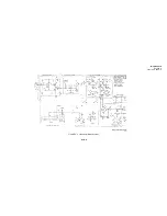
The four functional sections of the Model 5261A
are illustrated in Figure 5-4. The preamplifier, attenuator,
video amplifier, and output amplifier circuits are
combined to amplify AC signals as small as 1 millivolt
and provide a usable output level to the counter input
circuit. All dc voltages to operate the Model 5261A are
supplied from the counter in which the unit is installed.
These dc voltages are filtered by components on
Amplifier assembly A4, which includes a series regulator
in the 15-volt line.
4-3.
PREAMPLIFIER ASSEMBLY A1.
4-4.
The preamplifier circuit consists of a nuvistor
cathode follower driving an emitter follower to provide a
high impedance input and a low impedance output.
Diodes A1CR1 and A1CR2 limit input signal peaks and
prevent damage to A1Q1. Resistor A1R4 limits A1Q1
gate current during overload. Capacitors A1C2, A1C3,
A1C4, and A1C5 filter variations from the dc voltage
lines.
4-5.
ATTENUATOR SWITCH ASSEMBLY A2.
4-6.
Resistive attenuator A2 reduces the input signal
and establishes the overall gain of the Video Amplifier.
The amount of attenuation inserted is controlled by the
Video Amplifier SENSITIVITY switch. RC networks
A2C2, A2R10, and A219, A2C1 are selected to improve
frequency response.
4-7.
VIDEO AMPLIFIER ASSEMBLY A3.
4-8.
The video amplifier consists of two amplifiers
with three transistors each and feedback and drift
compensation for gain stability Feedback is provided by
the RC combination of A3R5, A3C4, A3R13, A3C1 and
transistors A3Q3, A3Q6 in the feedback loops of the two
amplifiers. Drift compensation is also accomplished with
the addition of A3Q3 and A3Q6. Positive feedback to
amplifier No. 2 from output amplifier A4Q4 increases
amplifier No. 2 gain at higher frequencies.
4-9.
The addition of A3Q3 and A3Q6 in the feedback
loops of the two amplifiers provides three functions: 1)
act as negative feedback amplifiers to reduce the gain
which reduces any drift caused by temperature changes
in the two-stage amplifiers; 2) maintain the amplifier gain
at low frequencies; and 3) filter ripple on the -14 volt line,
in conjunction with A3C6 and A3C13.
4-10.
OUTPUT AMPLIFIER ASSEMBLY A4.
4-11.
Output amplifier assembly A4 consists of: 1)
output amplifier circuit, 2) meter circuit: 3) plus 20volt
filter; and 4) series regulator. These four circuits are
discussed in Paragraphs 4-12 through 4-15.
4-12.
OUTPUT AMPLIFIER. Emitter follower A4Q4
provides the amplified input signal to the counter via rear
panel plug P6, pin 1. This same signal is supplied to
OUTPUT 509 jack J2 for monitoring with an oscilloscope
or application to other equipment. Positive feedback
from A4Q4 emitter to amplifier No. 2 in the video
amplifier assembly increases the video amplifier gain at
higher frequencies. Capacitors A4C9 and A4C10 are
connected in parallel to improve the overall frequency
response.
4-13.
METER CIRCUIT The signal atA4Q4 emitter is
rectified by A4C R2 and A4C R3 and filtered by A4C12.
This dc is supplied to OUTPUT LEVEL meter M1.
Capacitors A4C11 and A4C13 are connected in parallel
to improve the frequency response of the meter circuit.
Meter Cal potentiometer A4R13 provides an adjustment
for calibrating the OUTPUT LEVEL meter(Paragraph 5-
12). Minus 15 volts is supplied to the meter circuit and
establishes a bias on diodes A4CR2, 3. This prevents
the meter indicating for very small output signals and
permits a meter indication in the green scale for ml
output signal greater than 100 millivolts. Diode A4CR4
acts to protect the meter during input signals greater than
100 mv. A4CR4 anode is clamped at about -1.5 volts,
which corresponds to approximately full scale. When
the rectified signal output exceeds this value, A4CR4
conducts and protects the meter.
4-14.
PLUS 20 VOLT FILTER. Transistors A4Q1,
A4Q2, and associated components filter variations and
noise from the t 20-ivolt line. A voltage change at A4Q1
collector causes a change at A4Q2 base and A4Q2
changes conduction to oppose the variation. The
emitter-collector voltage drop across A4Q2 is
approximately 1 volt and the ,20 volts becomes t 19 volts
at the drain of FET A1Q1. Resistors A4R2 and A4R3
form a dc voltage divider to establish the quiescent
voltage at A4Q1 base. Capacitor A4C2 bypasses to
ground ac variations at A4Q1 base.
4-15.
SERIES REGULATOR. Series regulator A4Q3
provides regulated -14 volts for the Model 5261Acircuits.
Breakdown diode A4CRI establishes a reference voltage
at A4Q3 base. When the -15 volts changes, A4Q3
senses this change through A4R4 and increases
conduction to oppose the change. Inductor A4L1
reduces high-frequency transients in the -14 volt
regulated output.
4-1
Summary of Contents for AM-4380/U 5261A
Page 2: ...A ...
Page 7: ...Model 5261A Section I Figure 1 1 FIGURE 1 1 Model 5261A 1 0 ...
Page 19: ...Model 5261A Section V Figure 5 1 FIGURE 5 1 Schematic Diagram Notes 5 5 ...
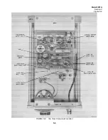
Page 20: ...Model 5261A Section V Figure 5 2 FIGURE 5 2 Top View Component Location 5 6 ...
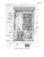
Page 21: ...Model 5261A FIGURE 5 3 Bottom View Component Location 5 7 ...
Page 22: ...Model 5261A Section V Figure 5 3 and 5 4 FIGURE 5 4 Video Amplifier Schematic 5 7 5 8 ...
Page 31: ...TM 11 6625 2906 14 P APPENIDIX C Additional Authorization List Not Applicable C 1 ...
Page 39: ...Model 5261A Appendix E FIGURE A 1 Top View Component Location E 3 ...
Page 40: ...Model 5261A Appendix E FIGURE A 2 Bottom View Component Location E 4 ...
Page 41: ...Model 5261A Appendix E FIGURE A 3 Video Amplifier Schematic E 5 ...
Page 42: ...Model 5261A Appendix E FIGURE A 4 A1 Preamplifier Component Location E 6 ...
Page 43: ...Model 5261A Appendix E FIGURE A 5 Video Amplifier Schematic E 7 ...
Page 44: ......
Page 45: ......
Page 47: ......
Page 48: ...PIN 046855 000 ...


