background image

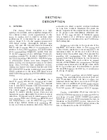
Circuit  Description 

C. 

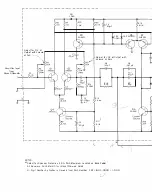
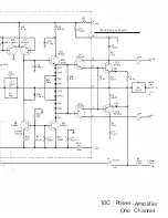
POWER AMPLIFIER 

The 

the  power  amplifier  is 

emitter  follower  com-

prising  transistors  Q12*  and 

*,  with  QlO  and 

as  their  drivers. 

point 

is 

provided 

resistors R5* and R6* and by currents 

from  current  source  Q8 

through 

CR9,  R22,  CR8  and  CR6. The power diodes  CRI * 

and  CR2*  shunt  R5*  and  R6*  at 

signal levels 

to  avoid 

voltage  drops  in  these  resistors. 

Inductance  L1 *  protects  the  output 

from 

the  effects  of 

cable  loads  at  very 

while  R8*  eliminates  any  series  reson­

ance with this capacity. Diodes 

CR12 

and  CR13  provide  output  current  limitation.  To-

with  fuses  F*  these 

output  short 

circuit 

The  output  stages  are  driven 

emitter  follower 

which  has  current  limita-

tion  in  the  collector. 

The  input 

consists  of  a  differential pair, 

and  Q2,  whose emitter currents are  supplied by 

The  input  signal  is  applied  to  the  base  of  Ql 

and  the  feedback  to  the  base  of  Q2.  The  output 

collector  swing  of  Ql is limited 

CR2  and  CR3 

to 

the  emitter-base junctions of the second 

and  Q7. 

The 

at  d-c  and  low 

is 

(  > 

100  dB).  The  primary  cutoff 

at 

frequencies  is  the  base-

Thus  the  loop 

falls  at  6  dB/octave  to  reach  a  value  of  about  60 

dB  at  10  kHz.  Inductors  Ll  and  L2  introduce  a 
second  pole  at  16  kHz  above  which  the 

gain 

falls  at  12  dB/octave  to  about  200 

where 

C6  begins  to  shunt  Rl6 

end cut-

off  in  the  amplifier  and  reducing  the  loop 

cutoff  rate  to  6 

once  more.  Gain 

crossover  is  at  about  1  MHz. 

The  bridged-T  comprising  C3, 

Rll,  and 

R12  increases  the 

below  16  Hz  and 

reduces  the  external 

at  d-c.  The 

are 

complex  so 

the  low  end  response  rises 

at  the  low  end 

before  dropping  off.  In  the  bass-boost  position 
C7  and  C8 

with  Rl6  and  R17  produce 

a pole  at  16  Hz and a zero  at 80 Hz in  the external 

most 

Thus  the  gain  rises  at  6 

below  80 

for  the  low  end  roll-off  of 

'Located  on  chassis.  See  righthand  portion  of  Power  Amplifier 

Schematic,  Section  VI, 

C. 

5-2 

The 

Oliver Audio  Amplifier 

Transistor  Q3 

current to two poten-

tiometers  R4  and 

which  are 

so that 

the  currents  through  R2  and  R3  supply  the  base 

currents  of  Ql  and  Q2. 

R5  with  the 

input  terminals  shorted 

control  at  mini-

and  R4  with  the 

terminals  open  (or 

with  the  volume  control  at  maximum)  to  give 
zero  volts  out  of  the 

this  condition  will 

hold  for  any 

faces  (any 

volume  control 

D. 

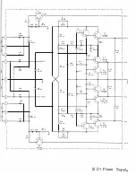
POWER  SUPPLY 

All  supply 

are  available  in  both 

(± 

40V)  is  rectified  by  diodes 

and  CR4  in  a  double  full  wave  configuration. 

Filtering  is 

capacitors  C3  and  C4.  This  supply 

has  a substantial amount of ripple, 

under 

but  the  power 

is  such 

that  this 

negligible  hum  in the 

-WARNING-

The  terminals  and  leads  of  C3  and  C4  are 

not  current 

Do  not  short  to 

or  to  each  other.  (You'll  ruin  your 

The 

supplies  are 

10V 

floated  on  the 

supplies  respectively. 

will  show  about  the same ripple as the latter. Tran­
sistors  Ql  and  Q2  with  their  associated  circuitry 
provide 

current  limits  on  the 

Zener  diodes  CR13  and  CR14  establish  the 

reference  voltages  for  the 

± 

20V  supplies  obtained 

from  the  cascaded  emitter  followers  Q3-Q5,  and 
Q4-Q6.  The  rate  of  rise  and  fall  of  these 

tum  on  and  tum  off  is determined  by  the 

active  filters  comprising 

Rl3 

R15,  C7  and  transistor 

for  the 

20V 

and  RIO,  C6,  Rl4  and 

C8,  and 

for  the  -20  V 

Diode  CR17 

for 

drops  in  Q5  and 

while  CR18  compensates  for  junction  drops  in 

Q6  and  Q8.  Resistors  Rll  and  Rl2 

for  the  initial 

currents  in  C5  and  C6  so 

that  these  currents  do  not  flow through  R17, 

CR17  and 

R20,  CRIS. 

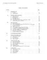
Summary of Contents for Barney Oliver

Page 1: ... 3 AMPLIfIER ...

Page 2: ...er Than Shure V 15 Type II G Installing in an Cabinet H Assem bly of Walnut or Teak Enclosure L Rack Cabinet J Pictures and Outline LOUDSPEAKER PHASING CIRCUIT DESCRIPTIONS A Phono B Filter Board C Power D Power CIRCUIT DIAGRAMS A Phono B Filter and Controls C Power one Channel Dl Power D2 E Sections PARTS A B C Power D P ower E Deck Parts B C and D Table of Contents Page 1 1 1 2 2 1 2 1 2 1 2 1 2...

Page 3: ...ter modulation distortion Since the are direct coupled overload no long time constant the are simply clipped and the original waveform resumes at its proper value immediately afterward Be cause of the amount of feedback only a fraction of a dB below actual overload typically show a total distortion over 75 dB below the fundamental networks in the fi circuits of the amplifiers and active filters in...

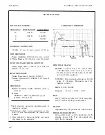
Page 4: ...ating simultaneously at maximum output Continuous high power operation at less than 8 n not recommended See instruction manual t Hum pickup by phono cartridge may cause this figure to be exceeded 1 2 FREQUENCY RESPONSE 15 15 I t H J t t f t lj c l H j CONTROLS Cont d FILTER Controls active h f roll off filter 18 dB octave with corner at 5 8 10 or 20 kHz Includes 30 dB notch at 10 kHz in 5 and 8 kH...

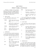
Page 5: ...reo channels reversed Left channel to right speaker right channel to left J Direct Each stereo channel to corresponding jJ an a Normal position CONTRO S DUAL Both channels mixed and deliv ered to both IJ LO L R The L Monophonic of left channel over both speakers Monophonic channel speakers allow of over both and other sources to be reproduced over either one STEREO or both MONO side p U vL C FILTE...

Page 6: ...as Deutsche conscientiously adhere to R IAA spec while others on 2 2 The Barney Oliver Audio Amplifier enhance the high end to compensate for the deficiencies of the usual playback If your are the 6 dB will help correct this If you find the 6 dB position better in the majority of cases your J o n L your need attention BASS Switch FLAT BOOST Located below the FILTER control is the two position BASS...

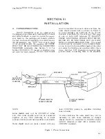
Page 7: ... BY PRYING THEM OUT AND OFF WITH A LARGE NEEDLE OR PICK The overall shield should be connected to the turntable frame at one end and to the amplifier chassis at the other end the post provided After this is done test that channels are isolated from ground before connecting them to the amplifier PHON6 0 1Npur I JACKS ON REAR l OF AMPLIfiER OUTER SHIELD NOTE TO GROUND CONNECTION ON REAR Of AMPLIfiER...

Page 8: ...information see Section V A LEFT SPEAKER The Barney Oliver Audio Amplifier C SPEAKER CONNECTIOI lS The amplifier may be located at any con venient distance from the loudspeakers Twisted pairs of No 18 wire or larger or ordinary zip cord may be used to connect the amplifiers to the speakers if the distance is under 100 feet For longer distances heavier conductors are recom mended In general the d c...

Page 9: ...drawing shown in III J Because certain components especially the power capacitors are quite large it will be seen that the overhang at the top of the front is not very great and at the bottom is virtu llly zero This Yill require considerable care in cutting the necessary hole in the cabinet It is strongly recommended that the amplifier be examined in detail before laying out this hole to prevent c...

Page 10: ...e slots just mentioned with the front edge fitting into a slot at the top rear of the front panel The rear edge of the top cover lies on the top of the back panel and is secured with a single 3 4 The Barney Oliver Audio Amplifier screw through the top cover It may be necessary to adjust the positions of the wood side panels to permit the top cover to slide into place without interference from side...

Page 11: ... ____ 10 93in 278 NOTE CASE IS AN EXTRA PRICE OPTION ...

Page 12: ...rces are heard independently Unless the are the above test is difficult but with identical the illusion is very and the test is easy to perform Reconnect the pre AMPLIFIER serving the proper This test need only be done once Return the MODE switch to the normal STEREO DIRECT If on the average one channel seems louder than the other throw the MODE switch to the STEREO REVERSE If the loud channel shi...

Page 13: ...e projected circuit zero in all directions the conductors and by shown This minimizes the to the power transformer and reduces the hum below audibility you notice any hum it s from directly to the cartridge Because the 10 K J cable impedance is low about has no effect on the up to 10 or 20 feet high end response for aepel 1Ultng on the cable used Many of the components that may you such as Q3 or C...

Page 14: ...ff In the bass boost position C7 and C8 with Rl6 and R17 produce a pole at 16 Hz and a zero at 80 Hz in the external most Thus the gain rises at 6 below 80 for the low end roll off of Located on chassis See righthand portion of Power Amplifier Schematic Section VI C 5 2 The Oliver Audio Amplifier Transistor Q3 current to two poten tiometers R4 and which are so that the currents through R2 and R3 s...

Page 15: ...aken from emitter followers Q7 and CR15 and CRI6 provide short circuit pro tection and transistors Q9 and QI0 the emitters of and Q8 reverse voltage from shorts betw een the 10 and 20 volt The 10 and 20 volt essentially ripple free The maximum various U JIJ HO 20V 40V 50V Circuit Description are l8 ma 70 ma 3 amps 0 5 amps and of the 5 3 ...

Page 16: ...eTION V I IR UIT DIAGRAMS ...

Page 17: ... 6db 0 R1AA r I i I I I I I I I I I I I I I I I i I I I 2 I I I I I I I I 3 I 4 I I I I I I I I 14 6dh I I R2 20 R4 511 0 R5 5110 C2 300J1 F NP 03 3 020 C6 151 R7 lOOK RS lOOK CR2 1 040 01 4 221 CR4 1 040 C1 30pF R6 10 n LOOP L __ _ ...

Page 18: ... 071 T Cii 1000pF 09 4 071 CR7 1 040 R22 RI7 10K 200 11 CR6 1 040 CRe 1 040 R20 011 4 071 010 3 020 CI2 15 fLF R27 51 1 1 R28 21 5K 17 OUTPUT TO SELECTOR SWITCH ________ _r _ t_ 2 1 1 1 1 _ _o 20V C5 300fLF NP LOOP RIO 20 0 LOOP I I I I I I I I I I __ _______________ ___________________ ____ ____ _J RI J Q 10 6 100Re 20K 75 Lo IN H Re IN 1 5mV PRODUCES 1 VOLT OUT AT I KHz ALL RESISTORS ileW METAL ...

Page 19: ...NER OUTPUT r I I II I I I I I I I 2 I I I I I I I 23 7K I I I I I I 221 I I I I i I I I I I I I I I I I I I R2 23 7K I L _ _ 20V rTOV IOV RUMBLE FILTER AND BUFFER AMP 20V IOV IOV MODE r i1 R 52 o o 0 FILTER 8 10 5 20 r I S3 I I I I i I I I RI3 21 3 16K S3A ...

Page 20: ...I I 1 I I I I I I I I I I ___ J Notes RIA TO POWER AMP PNP 2N3906 2N3904 This Boo d Util zes Two Seporate Connectors the Connector are Labled 1 thru 22 the Connector are Shown as 1 on on All Resistors lIS W Meta Fiim Oiherwise Noted C27 and C2S Selected To Center 0 KHz Notch 01 10KHz 100Hz ...

Page 21: ...for 0V at Output with Volume at Zero C6 CB 120pF 027fJ F RI6 5 11K R17 20K C3 R15 T l00f LF 34 BK _ NP C2 R14 5 IJ K 50f LF I I 10 t NOTES Select for Speaker Protection 2 0A 3AG Maximum Located on Back Pafe All Resistors lISW Metal Film Unless Otherwise Noted 16 4 Digit Number by Diodes is Derived from Part Number CRJ 1901 0040 J 040 J Q6 2N5551 RI9 5 11K Q7 2N5401 1 ...

Page 22: ...R22 75Jl R23 909Jl R26 10K I R28 R27 100 I I 13 50V 1 5 100 5 t l v 50V These Parts on Chassis R2 1 96K S5 ____________________________________________________ ___ BOOST FLAT R7 05 0 JlIC Power One 40V lD o J5 Ll Audio Out R8 J7 PI 51 1 0 J6 R9 100 0 1 2W OV o 40V Phone Jack J8 Amplifier Channel ...

Page 23: ...V Models Only For 115 230V Models See 1lI 02 4 Digit Number By Diodes and Transistors is Derived from Pari Number 01 1853 0045 3 045 All Resistors 1 8 W Melal Film Unless Otherwise Noted Rl lon R2 Ion OJ 2N4036 3 R CR9 CRll 26 C1 350fLF eRIO CR12 Q2 R 26 ...

Page 24: ...fLF Ril 42 2K RI2 42 2K C6 IOO fLF RI4 22K RIO 23 7K RS 562Jl R6 562Jl RI5 2K CRI3 21 5V CR14 21 5V RI6 2K 03 4 071 CRI5 9V RI7 IK CRI7 CRIB RI8 IK Cli J OOOpF C9 1000pF C I O 1000 pF R21 05 2N2405 4 352 560 07 2N2405 4 352 09 2N4036 3 045 010 2N2405 4 352 R23 10K R24 10K R25 10K 20V I I I I I I I I 10V r O l0V 08 2N4036 3 045 06 2N4036 3 045 R26 10K 20V 50V I 02 _ __ _________ 2 i___ ____________...

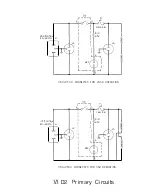
Page 25: ...I I O SA S 8_ I I I I RIO I I 47K I I J2 I I J3 I I I 1 I I L 4 I I I NEZ I I I L ___ _J 5 115V 230V CONNECTED FOR 230V OPERATION I L6A S B I I RIO I 47K I J2 I J3 I I L 4 I NEZ I I _ J 5 115V1230V CONNECTED FOR 115V OPERATION 02 rimary Circuits ...

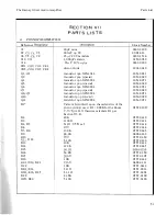
Page 26: ...stor npn X2N3904 transistor pnp aU i Ji npn X2N3904 TS upon characteristics of the used R l 909K for the Shure II Otherwise calculate R1 per Section D 20K 1 1 00 n 5 1 10 W m f lOOK 46 4K 5 11 K 1 0 K 120K 56 2K o 1 0 K o 1 0 K 5 1 10 5 1 1 0 2 1 5 K 5 1 1 K Parts List Stock Number 0160 2199 30D1614 0180 1746 01 50 0050 0160 0303 1901 0040 1854 0221 1853 0020 1854 007 1 1853 0020 1854 0071 1853 00...

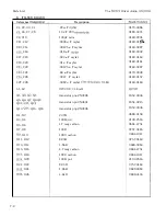
Page 27: ... 68 Jl F mylar 0170 0039 C26 0047 F mylar 0160 0157 C27 C28 0082 Jl F mylar VI B 0160 0160 L2 31 6 mH transistor pnp 2N3906 1853 0036 Q9 transistor npn 2N3904 1854 0215 Q13 Q15 Q16 transistor pnp 2N3906 1853 0036 R1 R2 23 7K 0698 3158 R3 R4 lOOK 2100 2516 R5 R6 4 7 meg carbon 0684 4751 R7 R8 lOOK 0757 0465 RIO lOon carbon 0684 1011 R11 R12 82 5K 0757 0463 R13 RI4 1 96K 0698 0083 R15 R16 4 7 meg ca...

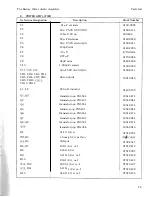
Page 28: ... 36pF mica 0160 2308 1 OOOpF ceramic 0150 0050 50p F 50V 0180 0141 silicon diode 1901 0040 220 I H inductor 9 140 0129 transistor npn 2N5551 1854 0474 transistor pnp 2N5401 1853 0264 transistor npn 2N5551 1854 0474 transitor pnp 2N5401 1853 0264 transistor npn 2N5551 1854 0474 transistor pnp 2N5401 1853 0264 transistor npn 2N5551 1854 0474 transistor pnp 2N4036 1853 0045 51 Ul 1 8 w 0757 0394 1 5 ...

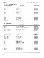
Page 29: ... 15V electrolytic 15000 F 50V Sprague electrolytic 100 F 15V electrolytic 1000pF ceramic diode rectifier 3 amp 100V diode rectifier amp 100V diode silicon diode Zener 21 5V diode Zener 9V diode silicon transistor pnp 2N4036 transistor npn 2N2405 transistor npn X2N3904 transistor pnp special transistor npn 2N2405 transistor pnp 2N4036 transistor npn 2N2405 transistor pnp 2N4036 transistor npn 2N240...

Page 30: ...5V 8A slo blo for 230V fuses 2 amp max AC power connector power line fuse holder nut washer fuse phono ring tip sleeve with phono preamp p c connector 18 pin power p c connector 18 filter and control p c connector 27 filter and control p c connector 10 pin fibre washers Parts List Stock Number 0757 0346 0698 3159 0757 0815 0698 31 8 0698 3450 0684 2231 0698 0083 0757 0280 0757 0815 0757 0442 Stock...

Page 31: ...ped attenuator 1 96 K lOQ 2w 8 2 Q 1h w 0 5 Q 5 1 1 Q w 100 n 1f 2 w 4 7 K w 3 16K 1 8 w 1 0 K 1 8 w input switch mode switch filter switch phono switch bass switch off on switch w pilot lamp 1 20 0 0043 special Cinch Jones P 202 CCT Motorola MJ4502 Motorola MJ80 2 D aven CPD 134 M H 4C687P 2dB step with detents 0698 0083 0698 360 1 0699 0003 0811 1826 07 57 1000 0757 0 1 9 8 0684 47 1 0757 0279 0...

Page 32: ... re c t io n s to A mplifie r IVlanual The follow ing corre c tions should be made to the B a r ne y Olive r A mp lifie r Manua l Page 7 2 C l l C 1 2 Page 7 3 P age 7 4 P age 7 6 Part N o should r e ad 0 1 6 0 0 1 5 6 R 2 H 3 Part N o should read 0 6 8 4 1 5 5 1 C R 9 1 0 1 1 1 2 Part No should read 1 9 0 1 0 0 4 0 R 2 7 R 2 8 Part No should re ad 0 6 8 4 1 0 1 1 R I O Part No should read 0 6 8 4...

Page 33: ... sure the p ickup c a r t riuge has fou r indepe ndent te r m in a l s w i th no metal o r w ire conne c tion between any two te r m ina l s 01 be twe e n any te rminal anu the me ta lli c case of the p ic k u p See S e c t ion I I I A 2 Make ce rt3 i n the re are separate s h ie ld e d le ads rom each s ide channe l of the p ic ku p c a r t idge 3c su re the re is no conne c tion be t w e e n lea...

Reviews: