


Introduction
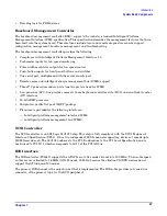
System Board Components
Chapter 1
22
System Board Components
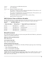
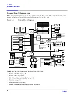
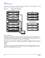
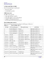
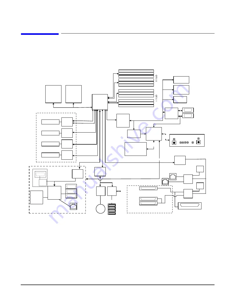
This section provides a block diagram of the system board and descriptions of key components (integrated
circuits) on the board. Figure 1-4 shows a block diagram of the rx2620 server.
Figure 1-4
System Block Diagram
The following describes the main components of the system board:
•
“Processor Sockets” on page 23
•
“Processor Bus” on page 23
•
“ZX1 I/O and Memory Controller” on page 23
•
“Memory” on page 23
•
“I/O Bus Interface” on page 25
•
“Processor Dependent Hardware Controller” on page 26
SCSI BACKPLANE
SCSI ID 0
SCSI ID 1
SCSI ID 2
(SE-LVDS SCA-2 80pin)
HDD #3
HDD #2
HDD #1
LED STATUS PANEL
ASIC
Bus
Interface
Industry Standard DDR1 DIMM
DIMM
FMW/PDC
Flash
16MB
FMW SRAM
(on battery, scratch
RAM + NVM)
512KB
RTC
BMC
Manageability
Controller
PDH Bus
FPGA
LPC + ACPI
I2C, etc...
SCSI
U320
LAN
10/100/
1G
external
(se-lvds 68p)
USB
2.0
IDE
DVD RW
Slim
Line
PCI 33/32
I2C
etc...
Itanium-2
IPF
Itanium-2
IPF
DMD
BMC SRAM 512KB
(on battery, scratch RAM•
+NVM+ FPL •
forward progress log)
BMC FLASH 1MB
Channel B
Channel A
Keyboard
Mouse
267MHz
8.5GB/S Peak Data BandWidth
267MHz 8b data
533MB/s Peak Data
Bandwidth per rope
133 MHz bus clock
267 MT/s data rate
8.5GB/s peak data bandwidth
DUART
System/BMC
Console
& Serial Port
Serial Port
OS Enabled
ON-OFF
ROPE 1
ROPE 4
ROPE 5
ROPE 3
ROPE 2
ROPE 6
ROPE 7
MEMORY
LPC
Bus
DIAG LEDs
LAN
Activity
LOCATOR
COM2
COM1
BMC
bus
Management Processor
RMC/GSP
Battery•
SRAM
DRAM
Flash
etc...
LAN100BT
Console
Modem
SCSI
U320
LAN
10/100/
1000
External
(SE-LVDS 68p)
PCI-X 133
PCI-X 133
PCI-X Interface
"Slot1"
PCI-X 133 "Slot2"
PCI-X 133 "Slot3"
PCI-X 133 "Slot4"
To AGP
Riser
FLASH
200MHz
6.4GB/S Peak Data BandWidth
FLASH
ROPE 0
UPS
PCI 33/32
VGA
VGA
Optional
DIMM
DIMM
DIMM
DIMM
DIMM
DIMM
DIMM
DIMM
DIMM
DIMM
ASIC
Bus
Interface
ASIC
Bus
Interface
ASIC
Bus
Interface
ASIC
Bus
Interface
ASIC
Bus
Interface
ASIC
Bus
Interface
ASIC
Bus
Interface
ASIC
Bus
Interface
iLO MP
8 MB


