


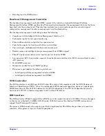


Introduction
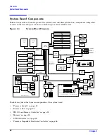
System Board Components
Chapter 1
25
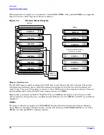
DIMMs are loaded in groups of four, known as a quad. All four DIMMs in a quad must be the same size.
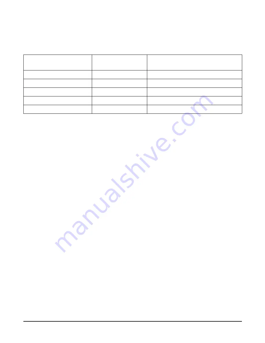
Table 1-2 summarizes the memory solutions.
Chip Spare Functionality
Chip spare enables an entire DDR SDRAM chip on a DIMM to be bypassed in the event that a multi-bit error
is detected on the DDR SDRAM. In order to use the chip spare functionality on your server, only DIMMs built
with
×
4 DDR SDRAM parts can be used, and these DIMMs must be loaded in quads.
The memory subsystem design supports the I/O ASIC chip’s spare functionality. Chip spare enables an entire
SDRAM chip on a DIMM to be bypassed/replaced in the event that a multi-bit error is detected on that
SDRAM. In order to use the chip spare functionality on, only DIMMs built with x4 SDRAM parts can be used,
and these DIMMs must be loaded in quads (two DIMMs per memory cell, loaded in the same location in each
memory cell). Each DIMM within a quad must be identical to all the other DIMMs in the quad.
Chip spare is achieved if four identical DIMMs are loaded into a quad. If more DIMMs are added, they must
be loaded in quads in order to maintain the chip spare functionality. So, if more DIMMs are added in to the
example case, four identical DIMMs (identical to each other, but can be different from the original quad that
was loaded) must be loaded into the next quad. However, if you are using 4 GB DIMMS, the only
configuration supported is eight 4 GB DIMMS in the first three quads, with no other DIMMs in the remaining
quad. For slot and quad locations, see Figure 4-23 on page 66.
Serial Presence Detect
Each DIMM contains an I2C electronically erasable programmable read-only memory (EEPROM) whose
content describes the module's characteristics: speed, revision, vendor, etc. This feature is called serial
presence detect (SPD). Firmware typically uses this information to detect unmatched pairs of DIMMs, and
configure certain memory subsystem parameters. The SPD information for DIMMs loaded in the server is
also accessible to the BMC through the I2C bus.
I/O Bus Interface
The I/O bus interface provides these features:
•
Industry standard PCI 33 MHz and 66 MHz, PCI-X 66 MHz to 133 MHz, 32 or 64 data bit support
•
3.3 V PCI only, it does not support 5 V PCI.
•
Optimizes for DMA performance.
•
Supports 3.3 V or Universal keyed PCI cards. 5 V keyed PCI cards are not supported
•
Supports up to four PCI sockets.
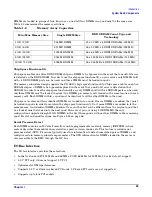
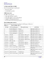
Table 1-2
Memory Array Capacities
Min / Max Memory Size
Single DIMM Size
DDR SDRAM Count, Type and
Technology
1 GB / 3 GB
256 MB DIMM
18 x 32 MB x 4 DDR1 SDRAMs (128 MB)
2 GB / 6 GB
512 MB DIMM
36 x 32 MB x 4 DDR1 SDRAMs (128 MB)
4 GB / 12 GB
1024 MB DIMM
36 x 64 MB x 4 DDR1 SDRAMs (256 MB)
8 GB / 24 GB
2048 MB DIMM
36 x 128 MB x 4 DDR1 SDRAMs (512 MB)
32 GB / 32 GB
4096 MB DIMM
36 x 256 MB x 4 DDR1 SDRAMs (1024 MB)