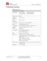
background image


MS2131 


Hardware Design Guide 


Issue 

02 

Date 

2017-1-13 


Summary of Contents for MS2131

Page 1: ...MS2131 Hardware Design Guide Issue 02 Date 2017 1 13 ...

Page 2: ... distribute modify decompile disassemble decrypt extract reverse engineer lease assign or sublicense the said software unless such restrictions are prohibited by applicable laws or such actions are approved by respective copyright holders Trademarks and Permissions and are trademarks or registered trademarks of Huawei Technologies Co Ltd Other trademarks product service and company names mentioned...

Page 3: ...E FORSEEABLE OR NOT THE MAXIMUM LIABILITY THIS LIMITATION SHALL NOT APPLY TO LIABILITY FOR PERSONAL INJURY TO THE EXTENT APPLICABLE LAW PROHIBITS SUCH A LIMITATION OF HUAWEI ARISING FROM THE USE OF THE PRODUCT DESCRIBED IN THIS MANUAL SHALL BE LIMITED TO THE AMOUNT PAID BY CUSTOMERS FOR THE PURCHASE OF THIS PRODUCT Import and Export Regulations Customers shall comply with all applicable export or ...

Page 4: ...t Issue 02 2017 1 13 Huawei Proprietary and Confidential Copyright Huawei Technologies Co Ltd 3 About This Document Change History Issue Date Chapter Note V1 0 2014 9 20 All Initial Release V1 1 2017 1 13 6 3 2 Modify Peripheral Staking Requirements ...

Page 5: ...2 1 USB Port and Reference Circuits 12 4 2 2 Power Port Introduction 13 4 3 SIM Card Port Introduction 14 5 MS2131 RF Features and Design Requirements 15 5 1 About This Chapter 15 5 2 Working Bands 15 5 3 Wireless Performance Specifications 16 5 3 1 TIS 16 5 3 2 TRP 16 5 4 Antenna Design Requirements 16 5 5 Antenna Test Environment 19 6 MS2131 Structure Features and Design Requirements 21 6 1 Abou...

Page 6: ...B Design Rules 31 8 2 Power Design 31 8 3 Cable Routing Rules 32 8 3 1 Power Design 32 8 3 2 USB Signal Cable Routing Design 32 8 3 3 Grounding Measure 33 9 MS2131 ESD Design Guide 34 9 1 PCB Design Recommendations for the Host 34 9 2 Shell Design Recommendations for the Host 34 10 MS2131 Electrical and Reliability Features 35 10 1 About This Chapter 35 10 2 Ultra Working Conditions 35 10 3 Workin...

Page 7: ...es The next five chapters describe the MS2131 s specifications and design requirements of its host Chapter 6 to Chapter 9 provide details of the MS2131 S working principles and design guides Chapter 10 introduces the MS2131 s electrical features and reliability Upon learning this document you will understand the MS2131 s port standards electricity supply characteristics design requirements and pro...

Page 8: ...al power supply requirement Strictly follow the design requirements in Chapter 7 when designing the power supply circuits Otherwise cases may occur that the board restarts in 2G large power events 2 The MS2131 has its antennas embedded Strictly follow the stacking design requirements in section 5 4 Antenna Design Requirements when designing a host Otherwise the antennas may deteriorate As a result...

Page 9: ... GPRS General Packet Radio Service GSM Global System for Mobile Communications The MS2131 supports the following services HSUPA based packet services HSPA UMT based high speed packet services EDGE GPRS based packet services WCDMA GSM short message service SMS The MS2131 can be connected to a host over a USB port to implement data card functions In the coverage area of the HSPA UMTS or EDGE GPRS GS...

Page 10: ...5 25 V 5 V is recommended Protocol WCDMA HSPA HSPA R7 AT commands For details see AT Command Interface Specification Application interfaces One standard SIM card slot 3 V or 1 8 V USB2 0 port Antenna interface Embedded FPC support antenna TS 5 external antenna port SMS Text messages in TEXT mode Data services WCDMA CS domain UL 64 kbps DL 64 kbps WCDMA HSPA PS domain DL 21 Mbps 64QAM UL 5 76 Mbps ...

Page 11: ...Confidential Copyright Huawei Technologies Co Ltd 10 3 4 Circuit Diagram The MS2131 contains the following functional modules as shown in Figure 3 1 Baseband processor BB and RF processor RTR Nand flash 19 2 MHz crystal resonator RF circuit Antenna USB2 0 port Figure 3 1 MS2131function block diagram ...

Page 12: ...l Copyright Huawei Technologies Co Ltd 11 3 5 Port Application Diagram The MS2131 contains the following ports as shown in Figure 3 2 USB2 0 port SIM card slot 1 8 V or 3 0 V TS 5 external antenna port Figure 3 2 MS2131 application diagram MS2131 Application interfaces USB SIM TS 5 SIM card External antenna RF ...

Page 13: ...cified design requirements when designing the interface circuits of a host 4 2 MS2131 Interface Introduction 4 2 1 USB Port and Reference Circuits The MS2131 communicates with the host over the USB port which supports the USB2 0 protocol The MS2131 has the USB signals adjusted and provides build out circuits The host must be able to perform impedance matching and protection Figure 4 1 shows the re...

Page 14: ...voltage range from 4 75 V to 5 25 V typical value 5 V Ensure that the power pins are properly connected during the use of the MS2131 as to maintain its normal performance When the MS2131 is dedicated for different applications attach importance to the power supply design In some network environments when the MS2131works at its largest power capacity for example when it works in GSM mode a USB volt...

Page 15: ...d Confidential Copyright Huawei Technologies Co Ltd 14 low dropout regulator LDO is used for the power supply the transient current capacity must be considered 4 3 SIM Card Port Introduction A standard SIM card port is embedded in the MS2131 The port supports the 3 0 V and 1 8 V SIM cards No external design is required ...

Page 16: ...MS2131 s wireless performance this chapter provides detailed requirements for the host layout and stacking design The antenna test environment is also introduced to help you understand the wireless performance test methods for the MS2131 5 2 Working Bands Table 5 1 describes the working bands that the MS2131 supports Table 5 1 MS2131 working bands Working Band Tx Rx UMTS Band I 1920 1980 MHz 2110 ...

Page 17: ...tant transmission performance specification of the MS2131 Table 5 3 describes the optimal TRP specifications of the MS2131 Table 5 3 MS2131 TRP specifications Frequency Band W2100 W1900 W900 W850 G1900 G1800 G900 G850 TRP specification dBm 18 16 5 18 16 5 22 5 24 27 25 5 The preceding TRP specifications can be realized only when the MS2131 is in optimal layout Therefore strictly follow the antenna...

Page 18: ...SB dongle and the metal 5 If there are other antennas in auxiliary devices the antennas must keep a distance from the USB dongle to avoid coupling 6 If the diversity antenna as in Figure 5 2 is in one side of the USB dongle the clearance opening should be faced outwards as shown in Figure 5 2 to ensure the optimal antenna performance 7 In order to minimize devices impact to the USB dongle corollar...

Page 19: ...gies Co Ltd 18 Figure 5 2 Recommended peripheral layout for the MS2131 Figure 5 3 Two common PCB layouts Layout 1 The USB dongle is embedded in the longer edge of the PCB Layout 2 The USB dongle is embedded in the shorter edge of the PCB If the terminal device is a rectangle such as a POS device the layouts shown in Figure 5 3 are recommended 1 L min L ...

Page 20: ...re the antennas are Strictly follow the antenna layout requirements and the stacking requirements specified in section 6 3 2 MS2131 Peripheral Staking Requirements when designing the system If you fail to follow the requirements the TRP and TIS specifications of the MS2131 will deteriorate and exceptions such as network access failures and call failures will occur 5 5 Antenna Test Environment The ...

Page 21: ...testing chamber system Auxiliary dedicated test platform Design the MS2131 dedicated test platform based on the stacking layout in Figure 5 2 Figure 5 6 shows the platform where a Thinkpad T61 is used This dedicated platform simulates the actual system layout to the maximum extent and all the tests and commissioning on the MS2131 are performed in the platform Figure 5 6 Dedicated test platform ...

Page 22: ... describes the MS2131 structure features including the system dimensions and design requirements addressing the host structure This chapter also describes the USB connector dimensions and its design requirements and guides addressing the host structure 6 2 Dimensions and Weight The MS2131 has dimensions of 84 9 mm x 27 mm x 12 3 mm including the USB cap and weighs about 30 0 g Figure 6 1 shows the...

Page 23: ...hnologies Co Ltd 22 6 3 MS2131 Design Requirements Addressing the Host Structure 6 3 1 USB Connector Outline Dimensions A standard USB2 0 connector shown in Figure 6 2 is used for the MS2131 The thickness of the PCB where the connector is inserted must range from 0 6 mm to 1 0 mm The recommended thickness is 0 8 mm Figure 6 2 USB connector for the MS2131 ...

Page 24: ...Hardware Design Guide MS2131 Structure Features and Design Requirements Issue 02 2017 1 13 Huawei Proprietary and Confidential Copyright Huawei Technologies Co Ltd 23 Figure 6 3 Dimensions of the USB connector ...

Page 25: ...31 is used with other device The USB interface between other device and the MS2131 the D D digital line and VBUS line must be routed at inner layer and packaged with the ground It recommended that the LC parallel resonant network should be reserved at the D D digital line of the USB interface which is between other device and MS2131 to reduce the influence of harmonics on low frequency It recommen...

Page 26: ...t be shielded and keep 10mm away from the side of the MS2131 If there are some clock circuit such as the TCXO circuit they must be shielded and keep 10mm away from the side of the MS2131 If there are other baseband signal processing circuit or control circuit they must be shielded and keep 10mm away from the side of the MS2131 If there are other RF communication unit such as WIFI BT GPS NFC and so...

Page 27: ...2G Mode This section describes the MS2131 power features when in use in 2G mode The power consumption of the MS2131 increases with its transmit power Transmit power also called uplink power is the amount of power used during transmission from a wireless terminal to a base station The Time Division Multiple Access TDMA uses GSM as the access method and therefore the MS2131 transmits signals only in...

Page 28: ...ode the uplink transmission occurs in two or more than two continuous slots as shown in Figure 7 2 Figure 7 2 GPRS working principle In GSM mode the MS2131 power transmission occurs in cycles and has transient changes during each transmission as shown in Figure 7 3 577uS 577uS 577uS x 8 slot 4 61ms 4 61ms 4 61ms Power Max 33dBm 577uS 577uS x 8 slot 4 61ms 4 61ms 4 61ms Power 1 15ms Max 30dBm ...

Page 29: ...quirement for the 2 A transient output within several microseconds There is output impedance at the MS2131 power connector and the currents are large When the transmission slot ends the GSM PA shuts down the power supply current then drops and the voltage resumes After 4 651 ms another transmission slot comes causing a voltage drop again Therefore the MS2131 operating in 2G mode must have good tra...

Page 30: ...pacity of 22 dB 5 V and less than 500 mA Power consumption in standby mode with a 3G network connected 5 V and less than 100 mA 7 6 Peripheral Power Design Requirements Power supplied to the MS2131 must have a minimum general current of 800 mA and a minimum transient current of 2 A The peripheral power design must be dedicated to these requirements to help the MS2131 bear the power supply voltage ...

Page 31: ...conductivity 7 6 3 Peripheral Power Supply Design Rules The peripheral power supply design rules for the MS2131 are described as follows 1 The power cable routing path must be as wide as possible to bear currents larger than 2 A during transmission in GSM mode 2 A large capacity capacitor at least 300 uF must be placed near the USB port to prevent its voltage from dropping lower than 3 5 V Energy ...

Page 32: ...surrounded by grounds and the impedance must be controlled in a proper range Do not interrupt the signal with strong interference or sensitive signals 8 2 Power Design The power design is a key factor for the MS2131 performance which has impacts on the following specifications EMC performance Radio modulation spectrum Phase and receiving sensitivity The general power design rules are described as ...

Page 33: ...f possible maximize the power cable routing width 8 3 2 USB Signal Cable Routing Design The impedance for the USB signal cable on the user PCB must be 90 Ω The impedance is dependent on the dielectric constant cable width and the distance from the ground Figure 8 1 and Figure 8 2 show the structures and stacking designs of the 90 Ω impedance microstrips and strip lines that can be adopted for the ...

Page 34: ...l Copyright Huawei Technologies Co Ltd 33 8 3 3 Grounding Measure To protect the USB signals from interference and sensitive sources surround the USB surfaces by grounds Ensure the continuity of reference grounds for all signal cables to avoid cross division Ensure a minimum loop path for each signal cable ...

Page 35: ...trical overstress EOS protection It is recommended that a component that has a peak power larger than 100 W at 8 20 µs be used 3 If the signal cable length is larger than 300 mm 12 inches surround the sides of the signal cables by grounds Drill holes on the grounds to connect them to the main ground 4 When connecting the host to the MS2131 ensure the grounding reliability 5 Use TVSs at the joint b...

Page 36: ...d reliability features of the MS2131 interfaces including Ultra working conditions Working and storage environment Power features Reliability features ESD features 10 2 Ultra Working Conditions Table 10 1 lists the working condition limitation for the MS2131 Permanent damage may be caused to the MS2131 if used beyond the conditions Table 10 1 Ultra working conditions of the MS2131 Symbol Parameter...

Page 37: ...e 10 3 lists the specifications for the MS2131 input power Table 10 3 Specifications for the MS2131 input power Parameter Minimum Value Typical Value Maximum Value Ripple Unit VBUS 4 75 5 5 25 50 mVpp 0 Hz to 2 5 GHz V 10 4 2 Working Current The MS2131 working current is specified in section 11 1 Appendix One MS2131 Power Consumption Data in Different Scenarios obtained from a test using direct cu...

Page 38: ...ration 11 ms 3 Shock times Six directions three times for each direction 18 times in total 9 Low temperature storage PASS 40 C for 24 hours with all specifications functions and mechanical performance remaining normal 10 High temperature storage PASS 85 C for 24 hours with all specifications functions and mechanical performance remaining normal 11 Low temperature operation PASS 20 C for 24 hours w...

Page 39: ...4 Test duration 168h 5 Test time point 48h 96h 144h and 168h 6 Restoration temperature and duration 25 C for 2h 18 Temperature cycle test PASS 1 Power on the sample Ensure the sample functions at a maximum transmit power 2 Temperature change ranges 10 1 C to 55 1 C 3 Temperature change rate 10 C min 4 Number of recycles 120 cycles one cycle including 30min at low temperature and 30min at high temp...

Page 40: ...o Ltd 39 The MS2131 has dedicated ESD requirements To ensure the proper connection between the MS2131 and the user interface board reference ground it is recommended that copper studs or other low impedance metal fasteners be used for the copper exposure to connect to an interface reference ground of the positioning holes on the user interface board CAUTION ...

Page 41: ...nfiguration HSDPA WCDMA UMTS bands 50 mA Power up and idle DRX cycle 8 2 56 sec 230 mA Phone call TX power 10 dBm 230 mA DL Rate 7 2 Mbps TX power 10 dBm GSM GPRS EDGE GSM bands 50 mA Power up and idle MFRMS 5 1 175 sec 140 mA Phone call TX power 10 dBm Table 11 2 Peak working currents in GPRS mode Bands Averaged Current Peak Current Units TX Power TX slot GPRS 850 230 1640 mA PCL 5 1 Up 1 Down GP...

Page 42: ...rent Units TX power dBm WCDMA Band I W2100 200 mA 1 230 10 400 22 Band II W1900 200 mA 1 230 10 300 22 Band V W850 200 mA 1 240 10 350 22 Band VIII W900 200 mA 1 240 10 380 22 HSDPA Band I W2100 220 mA 1 250 10 410 22 Band II W2100 220 mA 1 250 10 330 22 Band V W850 220 mA 1 250 10 380 22 Band VIII W900 220 mA 1 250 10 410 22 Values in Table 11 3 are average values obtained from a certain number o...

Page 43: ...50 4357 103 dBm 4408 4458 Band VIII W900 2937 102 dBm 3012 3088 GSM GSM 850 128 102 dBm 190 251 GSM 900 975 102 dBm 37 124 GSM 1800 512 103 dBm 698 885 GSM 1900 512 103 dBm 661 810 Values in Table 11 4 are average values obtained from a certain number of test samples which are tested in the stacking conditions shown in Figure 5 2 The tests are implemented with a PC If the stacking fails to meet re...

Page 44: ... 5 dBm 4183 4233 Band VIII W900 2712 19 5 dBm 2787 2863 GSM GSM 850 128 27 5 dBm 190 251 GSM 900 975 29 dBm 37 124 GSM 1800 512 24 dBm 698 885 GSM 1900 512 23 5 dBm 661 810 The preceding values are average values obtained from a certain number of test samples Figure 5 2 shows the MS2131 deployed in a PCB Samples are tested deployed in the board If the PCB is not designed as required in section 5 4...

Page 45: ...S2131 Hardware Design Guide Appendix Issue 02 2017 1 13 Huawei Proprietary and Confidential Copyright Huawei Technologies Co Ltd 44 11 3 Appendix Three MS2131 Thermal Test Thermal Test Report of Huawei M ...

Page 46: ...cess DL Down link DTE Data Terminal Equipment EDGE Enhanced Data Rate for GSM Evolution EMI Electro Magnetic Interference ESD Electro Static discharge GND Ground GPIO General purpose I O GPRS General Packet Radio Service GPS Global Positioning System GSM Global System of Mobile communication HSDPA High Speed Downlink Packet Access NC Not connected PCM Pulse code modulation USB Universal Serial BUS...

Reviews: