


MS2131
Hardware Design Guide
MS2131 Structure Features and Design Requirements
Issue 02 (2017-1-13)
Huawei Proprietary and Confidential
Copyright © Huawei Technologies Co., Ltd.
24
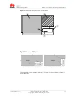
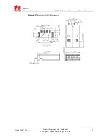
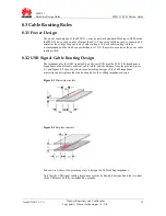
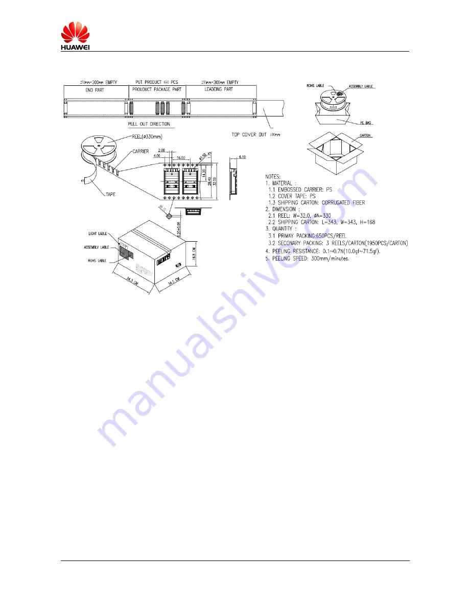
Figure 6-4
Package of the MS2131 USB connector (unit: mm)
6.3.2 MS2131 Peripheral Staking Requirements
When the MS2131 is used in conjunction with the other device
,
the customer must complete
the design in accordance with the following rules
,
otherwise it will affect the wireless
performance of MS2131. Detailed rules as follows:
·
The customer should be according to the requirements of antenna in section 5.4 to
complete the design firstly
,
when the MS2131 is used with other device.
·
The USB interface between other device and the MS2131
,
the D+/D- digital line and
VBUS line must be routed at inner layer and packaged with the ground.
·
It recommended that the LC parallel resonant network should be reserved at the D+/D-
digital line of the USB interface which is between other device and MS2131 to reduce the
influence of harmonics on low frequency.
·
It recommended that the two sides of the component of the interface should leakage of
copper on the PCB surface.
·
It recommended that the other high speed communication interfaces such as other USB
interface, SIDO, PCIE, MIPI and so on must be routed at inner layer and packaged with the
ground, and the component of the interface should be shielded
,
also we suggest the
component of the interface keep 10mm away from the side of the MS2131.