UHF1(400-470MHz)
Circuit Description
15
Clock
X1001
32.768KHz
1
2
20pF
20pF
APLL
ULPD
96MHz
DPLL1
OSC32K_OUT
OSC32K_IN
OSC1_OUT
OSC1_IN
CK_REF
19.2MHz
ARM_CK
DSP_CK
TC_CK
MCLK
OMAP3.2
ULPD_PLL_CLK
OMAP5912
TLV320AIC29
19.2MHz
MCLK
U1002
U801
CLK32K_IN
VSS(Y13)
VCC
VCC
OUT
VCONT
GND
X8001
TCXO 19.2MHz
1
2
3
4
Input Clock
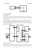
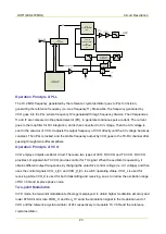
32K Clock: It is also called “sleep clock” and is mainly used for system timing and sleeping.
19.2 MHz System Clock: It is mainly used to provide the input clock for APLL and DPLL.
Output Clock
There is one output clock: MCLK. MCLK provides 16 MHz clock to audio codec.
Reset Signal
Flash
PsRAM
RESET IC
PWR-RESET
nRst_Out
CODEC
OMAP5912
Codec_nRst
SPI
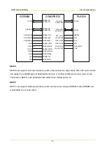
OMAP5912 has one SPI, which has four chip selects for connecting four external SPI components. The
available SPI signals are SPI.DOUT, SPI.DIN, SPI.CLK and SPI.CS. The system uses SPIF.CS2 to
select the IF processor AD9864, to configure the register of AD9864. The connection of SPI is shown
below.
Summary of Contents for PD502
Page 1: ...PORTABLE...
Page 5: ...VHF 136 174 MHz...
Page 13: ...VHF 136 174 MHz Exploded View and Packaging Guide 7 3 2 Packaging Guide...
Page 18: ...VHF 136 174 MHz Circuit Description 12...
Page 43: ...PCB 3 9 PCB VHF 136 174 MHz...
Page 44: ...PCB 3 VHF 136 174 MHz...
Page 71: ...UHF1 400 470 MHz...
Page 79: ...UHF1 400 470MHz Exploded View and Packaging Guide 7 3 2 Packaging Guide...
Page 84: ...UHF1 400 470MHz Circuit Description 12...
Page 108: ...UHF1 400 470MHz PCB 36 9 PCB...
Page 109: ...UHF1 400 470MHz PCB 37...
Page 136: ...1616300000260 2014 03 17 L07157 4...


